US9318599B2 - Power semiconductor device - Google Patents
Power semiconductor device Download PDFInfo
- Publication number
- US9318599B2 US9318599B2 US14/331,603 US201414331603A US9318599B2 US 9318599 B2 US9318599 B2 US 9318599B2 US 201414331603 A US201414331603 A US 201414331603A US 9318599 B2 US9318599 B2 US 9318599B2
- Authority
- US
- United States
- Prior art keywords
- region
- power semiconductor
- semiconductor device
- device protection
- drift layer
- Prior art date
- Legal status (The legal status is an assumption and is not a legal conclusion. Google has not performed a legal analysis and makes no representation as to the accuracy of the status listed.)
- Expired - Fee Related
Links
Images


Classifications
-
- H10P10/00—
-
- H—ELECTRICITY
- H10—SEMICONDUCTOR DEVICES; ELECTRIC SOLID-STATE DEVICES NOT OTHERWISE PROVIDED FOR
- H10D—INORGANIC ELECTRIC SEMICONDUCTOR DEVICES
- H10D30/00—Field-effect transistors [FET]
- H10D30/60—Insulated-gate field-effect transistors [IGFET]
- H10D30/64—Double-diffused metal-oxide semiconductor [DMOS] FETs
- H10D30/66—Vertical DMOS [VDMOS] FETs
- H10D30/668—Vertical DMOS [VDMOS] FETs having trench gate electrodes, e.g. UMOS transistors
-
- H01L29/7813—
-
- H01L29/0615—
-
- H01L29/1095—
-
- H01L29/4236—
-
- H—ELECTRICITY
- H10—SEMICONDUCTOR DEVICES; ELECTRIC SOLID-STATE DEVICES NOT OTHERWISE PROVIDED FOR
- H10D—INORGANIC ELECTRIC SEMICONDUCTOR DEVICES
- H10D12/00—Bipolar devices controlled by the field effect, e.g. insulated-gate bipolar transistors [IGBT]
-
- H—ELECTRICITY
- H10—SEMICONDUCTOR DEVICES; ELECTRIC SOLID-STATE DEVICES NOT OTHERWISE PROVIDED FOR
- H10D—INORGANIC ELECTRIC SEMICONDUCTOR DEVICES
- H10D12/00—Bipolar devices controlled by the field effect, e.g. insulated-gate bipolar transistors [IGBT]
- H10D12/411—Insulated-gate bipolar transistors [IGBT]
- H10D12/441—Vertical IGBTs
- H10D12/461—Vertical IGBTs having non-planar surfaces, e.g. having trenches, recesses or pillars in the surfaces of the emitter, base or collector regions
- H10D12/481—Vertical IGBTs having non-planar surfaces, e.g. having trenches, recesses or pillars in the surfaces of the emitter, base or collector regions having gate structures on slanted surfaces, on vertical surfaces, or in grooves, e.g. trench gate IGBTs
-
- H—ELECTRICITY
- H10—SEMICONDUCTOR DEVICES; ELECTRIC SOLID-STATE DEVICES NOT OTHERWISE PROVIDED FOR
- H10D—INORGANIC ELECTRIC SEMICONDUCTOR DEVICES
- H10D62/00—Semiconductor bodies, or regions thereof, of devices having potential barriers
- H10D62/10—Shapes, relative sizes or dispositions of the regions of the semiconductor bodies; Shapes of the semiconductor bodies
- H10D62/102—Constructional design considerations for preventing surface leakage or controlling electric field concentration
- H10D62/103—Constructional design considerations for preventing surface leakage or controlling electric field concentration for increasing or controlling the breakdown voltage of reverse-biased devices
- H10D62/105—Constructional design considerations for preventing surface leakage or controlling electric field concentration for increasing or controlling the breakdown voltage of reverse-biased devices by having particular doping profiles, shapes or arrangements of PN junctions; by having supplementary regions, e.g. junction termination extension [JTE]
-
- H—ELECTRICITY
- H10—SEMICONDUCTOR DEVICES; ELECTRIC SOLID-STATE DEVICES NOT OTHERWISE PROVIDED FOR
- H10D—INORGANIC ELECTRIC SEMICONDUCTOR DEVICES
- H10D62/00—Semiconductor bodies, or regions thereof, of devices having potential barriers
- H10D62/10—Shapes, relative sizes or dispositions of the regions of the semiconductor bodies; Shapes of the semiconductor bodies
- H10D62/113—Isolations within a component, i.e. internal isolations
- H10D62/115—Dielectric isolations, e.g. air gaps
-
- H—ELECTRICITY
- H10—SEMICONDUCTOR DEVICES; ELECTRIC SOLID-STATE DEVICES NOT OTHERWISE PROVIDED FOR
- H10D—INORGANIC ELECTRIC SEMICONDUCTOR DEVICES
- H10D62/00—Semiconductor bodies, or regions thereof, of devices having potential barriers
- H10D62/10—Shapes, relative sizes or dispositions of the regions of the semiconductor bodies; Shapes of the semiconductor bodies
- H10D62/124—Shapes, relative sizes or dispositions of the regions of semiconductor bodies or of junctions between the regions
- H10D62/126—Top-view geometrical layouts of the regions or the junctions
- H10D62/127—Top-view geometrical layouts of the regions or the junctions of cellular field-effect devices, e.g. multicellular DMOS transistors or IGBTs
-
- H—ELECTRICITY
- H10—SEMICONDUCTOR DEVICES; ELECTRIC SOLID-STATE DEVICES NOT OTHERWISE PROVIDED FOR
- H10D—INORGANIC ELECTRIC SEMICONDUCTOR DEVICES
- H10D62/00—Semiconductor bodies, or regions thereof, of devices having potential barriers
- H10D62/10—Shapes, relative sizes or dispositions of the regions of the semiconductor bodies; Shapes of the semiconductor bodies
- H10D62/13—Semiconductor regions connected to electrodes carrying current to be rectified, amplified or switched, e.g. source or drain regions
- H10D62/149—Source or drain regions of field-effect devices
- H10D62/151—Source or drain regions of field-effect devices of IGFETs
- H10D62/156—Drain regions of DMOS transistors
- H10D62/157—Impurity concentrations or distributions
-
- H—ELECTRICITY
- H10—SEMICONDUCTOR DEVICES; ELECTRIC SOLID-STATE DEVICES NOT OTHERWISE PROVIDED FOR
- H10D—INORGANIC ELECTRIC SEMICONDUCTOR DEVICES
- H10D62/00—Semiconductor bodies, or regions thereof, of devices having potential barriers
- H10D62/10—Shapes, relative sizes or dispositions of the regions of the semiconductor bodies; Shapes of the semiconductor bodies
- H10D62/17—Semiconductor regions connected to electrodes not carrying current to be rectified, amplified or switched, e.g. channel regions
- H10D62/393—Body regions of DMOS transistors or IGBTs
-
- H—ELECTRICITY
- H10—SEMICONDUCTOR DEVICES; ELECTRIC SOLID-STATE DEVICES NOT OTHERWISE PROVIDED FOR
- H10D—INORGANIC ELECTRIC SEMICONDUCTOR DEVICES
- H10D64/00—Electrodes of devices having potential barriers
- H10D64/20—Electrodes characterised by their shapes, relative sizes or dispositions
- H10D64/27—Electrodes not carrying the current to be rectified, amplified, oscillated or switched, e.g. gates
- H10D64/311—Gate electrodes for field-effect devices
- H10D64/411—Gate electrodes for field-effect devices for FETs
- H10D64/511—Gate electrodes for field-effect devices for FETs for IGFETs
- H10D64/512—Disposition of the gate electrodes, e.g. buried gates
- H10D64/513—Disposition of the gate electrodes, e.g. buried gates within recesses in the substrate, e.g. trench gates, groove gates or buried gates
Definitions
- the present disclosure relates to a power semiconductor device having a high level of reliability.
- a power semiconductor device has been widely used to control a motor or used in various switching devices such as an inverter, or the like.
- the power semiconductor device a semiconductor device used in a power apparatus
- the power semiconductor device is a core component of the power apparatus optimized for the conversion or controlling of power.
- the power semiconductor device has a high blocking voltage, a high current, and a high frequency as compared to a general semiconductor device.
- MOSFET metal oxide semiconductor field effect transistor
- IGBT insulated gate bipolar transistor
- Such an IGBT and MOSFET basically have an n-p-n junction structure. That is, since n-p-n junctions are formed between two diodes so that rectification directions are opposite to each other, current does not flow.
- Current may flow between an emitter and a collector or a source and a drain.
- the IGBT means a transistor manufactured so as to have bipolarity by forming a gate using a metal oxide semiconductor (MOS) and forming a p-type collector layer on a rear surface thereof.
- MOS metal oxide semiconductor
- an operational principle of the IGBT will be described.
- a voltage higher than a threshold voltage of the IGBT device is applied to a gate electrode, a polarity of a surface of a p-type body region positioned at a lower end of the gate electrode is inversed, and accordingly an n-type channel is formed, such that a current may flow between an anode and a cathode.
- An electron current injected into a drift region though the channel induces injection of a hole current from a high-concentration p-type collector layer positioned below the IGBT device, similar to a base current of the bipolar transistor.
- the IGBT may be used with very high voltages.
- IGBTs have characteristics such as a low forward loss and rapid switching speeds, the application of IGBTs to fields that may to which existing thyristors, bipolar transistors, MOSFETs, and the like, has increased.
- a power semiconductor device is composed of hundreds of thousands to millions of cells in a single device.
- a high degree of heat may be generated in a portion corresponding to a junction of the device.
- a temperature of the corresponding portion is increased to 1400° C. or more due to heat generated at the junction.
- a melting point of silicon (Si) is 1414° C., the corresponding portion of the device may be completely broken, such that the entire device may be unusable.
- Patent Document 1 A semiconductor apparatus has been disclosed in the following Related Art Document (Patent Document 1).
- Patent Document 1 A semiconductor apparatus having a high breakdown voltage has been disclosed in Patent Document 1.
- the semiconductor apparatus disclosed in Patent Document 1 is characterized in that carrier density may be increased in the vicinity of an emitter and a high breakdown voltage may be obtained by disposing an insulation layer between gate trenches arranged at a predetermined pitch.
- a region having electrical insulation properties is formed in advance, which is different from the present disclosure in that a device protection layer of the present disclosure may be a region capable of being electrically conducted before a high level of heat is generated due to latch-up or a short-circuit.
- Patent Document 1 Korean Patent Publication No. 10-0223198
- An aspect of the present disclosure may provide a power semiconductor device capable of cutting off a cell in which a problem occurs when a high level of heat is generated due to latch-up or a short-circuit at the time of an operation of the device.
- a power semiconductor device may include: a first conductive type drift layer in which trench gates are formed; a second conductive type well region formed on the drift layer so as to contact the trench gate; a first conductive type source region formed on the well region so as to contact the trench gate; and a device protection region formed below a height of a lowermost portion of the source region in a height direction.
- the device protection region may be formed below the source region.
- the device protection region may be formed in the well region.
- the power semiconductor device may further include a channel region formed in a portion of the well region contacting the trench gate when the device is turned on, wherein the device protection region is formed in a portion of the channel region.
- the device protection region may be formed in a portion at which the drift layer and the well region contact each other.
- the power semiconductor device may further include a channel region formed in a portion of the well region contacting the trench gate when the device is turned on, wherein the device protection region is formed below the channel region.
- the device protection region may be formed in the drift layer.
- the power semiconductor device may further include a channel region formed in a portion of the well region contacting the trench gate when the device is turned on, wherein the device protection region is formed below the channel region in the height direction.
- the device protection region may contain at least one of an oxygen atom and a nitrogen atom.
- the device protection region may be changed to have insulation properties when latch-up or a short-circuit occurs.
- a power semiconductor device may include: a first conductive type drift layer; a plurality of trench gates formed lengthwise in the drift layer to be spaced apart by a predetermined interval in one direction; a second conductive type well region between the plurality of the trench gates; first conductive type source regions formed in the well region to be spaced apart by a predetermined interval in one direction so as to contact the trench gate; and a device protection region formed below a height of a lowermost portion of the source region in a height direction.
- the device protection region may be formed below the source region.
- the device protection region may be formed in the well region.
- the power semiconductor device may further include a channel region formed in a portion of the well region contacting the trench gate when the device is turned on, wherein the device protection region is formed in a portion of the channel region.
- the device protection region may be formed in a portion at which the drift layer and the well region contact each other.
- the power semiconductor device may further include a channel region formed in a portion of the well region contacting the trench gate when the device is turned on, wherein the device protection region is formed below the channel region.
- the device protection region may be formed in the drift layer.
- the power semiconductor device may further include a channel region formed in a portion of the well region contacting the trench gate when the device is turned on, wherein the device protection region is formed below the channel region in the height direction.
- the device protection region may contain at least one of an oxygen atom and a nitrogen atom.
- the device protection region may be changed to have insulation properties when latch-up or a short-circuit occurs.
- FIG. 1 is a schematic cross-sectional view of a power semiconductor device according to an exemplary embodiment of the present disclosure
- FIG. 2 is a schematic cross-sectional view illustrating a state after a short-circuit or latch-up occurs in the power semiconductor device according to an exemplary embodiment of the present disclosure
- FIG. 3 is a schematic perspective view of a power semiconductor device according to a first exemplary embodiment of the present disclosure
- FIG. 4 is a schematic perspective view of a power semiconductor device according to a second exemplary embodiment of the present disclosure.
- FIG. 5 is a schematic perspective view of a power semiconductor device according to a third exemplary embodiment of the present disclosure.
- FIG. 6 is a schematic plan view of a power semiconductor device according to a fourth exemplary embodiment of the present disclosure.
- FIG. 7 is a schematic plan view of a power semiconductor device according to a fifth exemplary embodiment of the present disclosure.
- FIG. 8 is a schematic plan view of a power semiconductor device according to a sixth exemplary embodiment of the present disclosure.
- x, y, and z directions refer to a width direction, a length direction, and a height direction, respectively.
- a power switch may be implemented by any one of a power metal oxide semiconductor field effect transistor (MOSFET), an insulated gate bipolar transistor (IGBT), a thyristor, and devices similar to the above-mentioned devices.
- MOSFET power metal oxide semiconductor field effect transistor
- IGBT insulated gate bipolar transistor
- thyristor a thyristor
- Most of new technologies disclosed herein will be described based on the IGBT. However, several exemplary embodiments of the present disclosure disclosed herein are not limited to the IGBT, but most of the exemplary embodiments may also be applied to other types of power switch technologies including a power MOSFET and several types of thyristors in addition to a diode. Further, several exemplary embodiments of the present disclosure will be described as including specific p-type and n-type regions. However, conductive types of several regions disclosed herein may be similarly applied to devices having conductive types opposite thereto.
- an n-type or a p-type used herein may be defined as a first conductive type or a second conductive type.
- the first and second conductive types mean different conductive types.
- positive ‘+’ refers to the state in which a region is heavily doped and negative ‘ ⁇ ’ refers to the state that a region is lightly doped.
- FIG. 1 is a schematic cross-sectional view of a power semiconductor device 100 according to an exemplary embodiment of the present disclosure.
- a cross-sectional structure of the power semiconductor device 100 according to an exemplary embodiment of the present disclosure will be described with reference to FIG. 1 .
- the power semiconductor device 100 may include a first conductive type drift layer 10 in which trench gates 40 are formed; a second conductive type well region 20 formed on the drift layer 10 so as to contact the trench gate 40 ; a first conductive type source region 30 formed on the well region 20 so as to contact the trench gate 40 ; and a device protection region 50 formed below a height of a lowermost portion of the source region 30 in the height direction (z direction).
- the first conductive type may be an n-type, and the second conductive type may be a p-type.
- the drift layer 10 may have low-concentration n-type impurities in order to maintain a blocking voltage of the power semiconductor device.
- the well region 20 and the source region 30 may have a source metal layer (not shown) formed on exposed upper surfaces thereof.
- the drift layer 10 may have a buffer layer 11 formed therebeneath.
- the buffer layer 11 may be an n-type or p-type buffer layer, and in the case in which the buffer layer 11 is an n-type buffer layer, the buffer layer may be operated as a MOSFET, and in the case in which the buffer layer is a p-type buffer layer, the buffer layer 11 may be operated as an IGBT.
- the buffer layer 11 may have a collector metal layer 60 formed therebeneath.
- the trench gate 40 may be formed by etching the drift layer 10 , forming a gate insulation layer 41 , and then filling in the gate insulation layer 41 with poly silicon 42 .
- the device protection region 50 may be formed by injecting an oxygen or nitrogen atoms.
- the well region 20 may be formed so as to have second conductive type impurities and the source region 30 may be formed so as to have high-concentration first conductive type impurities.
- the source region 30 —the well region 20 —the drift layer 10 may have an n-p-n junction.
- the power semiconductor device 100 may have hundreds of thousands to millions n-p-n junctions, and a single n-p-n junction may operate as a single cell.
- the conductive channel is formed at the channel region 21 , such that the current may flow between the source metal layer (not shown) and the collector metal layer 60 .
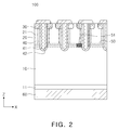
- FIG. 2 is a schematic cross-sectional view illustrating a state after a short-circuit or latch-up occurs in the power semiconductor device 100 according to an exemplary embodiment of the present disclosure.
- the portion of the device protection region 50 may be changed into an insulation region 51 , such that the cell is permanently cut off, thereby preventing breakage of the entire power semiconductor device 100 .
- junction breakage may occur.
- Junction breakage means that a high level of heat is generated in a portion at which the drift layer 10 and the well region 20 are bonded to each other, such that the corresponding portion is broken.
- the source region 30 —the well region 20 —the drift region 10 —the buffer layer 11 may have an n-p-n-p junction.
- the n-p-n-p junction may operate as a parasitic thyristor in the IGBT.
- a high level of heat may be generated in a portion at which the drift layer 10 of the cell in which the parasitic thyristor is turned on contacts the well region 20 , and furthermore, the cell may be broken, and the entire power semiconductor device 100 may be broken.
- a phenomenon that the parasitic thyristor is turned on, and thus, the power semiconductor device 100 is broken as described above is referred to as latch-up.
- a high level of heat may be generated in the cell, and furthermore, the entire power semiconductor device 100 may be broken.
- the device protection region 50 may be formed below a height of a lowermost portion of the source region 30 in the height direction (z direction).
- the device protection region 50 may be formed by injecting the oxygen or nitrogen atoms.
- a high level of heat of maximum 1400° C. or more may be generated in the cell corresponding to the portion at which the problem occurs.
- the device protection region 50 may be changed into the insulation region 51 formed of the silicon oxide or silicon nitride before a temperature of the portion at which the problem occurs reaches 1400° C.
- the silicon oxide or silicon nitride Since the silicon oxide or silicon nitride has insulation properties that silicon oxide or silicon nitride does not conduct electricity, the current flowing to the cell in which the problem occurs may be permanently cut off.
- the device protection region 50 may operate as a conductive region through which a current flows.
- the device protection region 50 since in the device protection region 50 after short-circuit or latch-up occurs, the oxygen or nitrogen atoms are bound to silicon to thereby be changed into a silicon oxide or silicon nitride state, the device protection region 50 may become the insulation region 51 through which the current does not flow.
- FIG. 3 is a schematic perspective view of a power semiconductor device 100 according to a first exemplary embodiment of the present disclosure.
- the power semiconductor device 100 may include an n ⁇ type drift layer 110 in which trench gates 140 are formed; a p0 type well region 120 formed on the drift layer 110 so as to contact the trench gate 140 ; an n+ type source region 130 formed on the well region 120 so as to contact the trench gate 140 ; and a device protection region 150 formed below a height of a lowermost portion of the source region 130 in a height direction (z direction), wherein the device protection region 150 may be formed at the all of the portions at which the drift layer 110 and the well region 120 contact each other.
- the device protection region 150 of the power semiconductor device 100 may be formed so as to be positioned between the drift layer 110 and the well region 120 .
- the device protection region 150 is formed at all of the portions at which the drift layer 110 and the well region 120 contact each other, reliability of the power semiconductor device 100 may be significantly increased.
- heat may be generated at the portion at which the drift layer 110 and the well region 120 contact each other, such that the corresponding portion may be broken by heat.
- junction breakage This phenomenon is referred to as junction breakage.
- the device protection region 150 is formed at the portion at which the drift layer 110 and the well region 120 contact each other, such that generation of the junction breakage as described above may be prevented.
- FIG. 4 is a schematic perspective view of a power semiconductor device 200 according to a second exemplary embodiment of the present disclosure.
- the power semiconductor device 200 may include an n ⁇ type drift layer 210 in which trench gates 240 are formed; a p0 type well region 220 formed on the drift layer 210 so as to contact the trench gate 240 ; an n+ type source region 230 formed on the well region 220 so as to contact the trench gate 240 ; and a device protection region 250 formed below a height of a lowermost portion of the source region 230 in a height direction (z direction), wherein the device protection region 250 may be formed in the well region 220 .
- the channel region 221 may be directly insulated.
- FIG. 5 is a schematic perspective view of a power semiconductor device 300 according to a third exemplary embodiment of the present disclosure.
- the power semiconductor device 300 may include an n ⁇ type drift layer 310 in which trench gates 340 are formed; a p0 type well region 320 formed on the drift layer 310 so as to contact the trench gate 340 ; an n+ type source region 330 formed on the well region 320 so as to contact the trench gate 340 ; and a device protection region 350 formed below a height of a lowermost portion of the source region 330 in a height direction (z direction), wherein the device protection region 350 may be formed in the drift layer 310 .
- the device protection region 350 may be formed by injecting oxygen or nitrogen atoms, a blocking voltage of the drift layer 310 may be improved.
- the device protection region 350 may improve the blocking voltage of the drift layer 310 as well as an effect of permanently cutting off the cell in which a problem occurs when the problem such as the short-circuit or latch-up occurs.
- FIG. 6 is a schematic plan view of a power semiconductor device 400 according to a fourth exemplary embodiment of the present disclosure.
- the power semiconductor device 400 may include an n ⁇ type drift layer; a plurality of trench gates 440 formed lengthwise in the drift layer to be spaced apart by a predetermined interval in one direction; a p0 type well region 420 formed between the plurality of trench gates 440 ; n+ type source regions 430 formed in the well region 420 to be spaced apart by a predetermined interval in one direction so as to contact the trench gate 440 ; and a device protection region 450 formed below a height of a lowermost portion of the source region 430 in a height direction, wherein the device protection region 450 may be formed below the source region 430 .
- the device protection region 450 may be formed below the source region 430 so as to correspond to a position of the source region 430 .
- the device protection region 450 is a region into which oxygen or nitrogen atoms are injected, when the power semiconductor device 400 is turned on, the device protection region 450 may increase turn-on resistance.
- an increase in the turn-on resistance of the power semiconductor device 400 may be prevented by forming the device protection region 450 below the source region 430 so as to correspond to the position of the source region 430 .
- the cell at which the problem occurs may be permanently cut off by the device protection region 450 , thereby preventing the entire power semiconductor device 400 from being broken.
- the device protection region 450 may be formed below the source region and formed at at least one of a portion at which the drift layer and the well region contact each other, the drift layer, and the well region, as in first to third exemplary embodiments.
- the resulting effect may be equal to that as described in first to third exemplary embodiments.
- FIG. 7 is a schematic plan view of a power semiconductor device 500 according to a fifth exemplary embodiment of the present disclosure.
- the power semiconductor device 500 may include an n ⁇ type drift layer; a plurality of trench gates 540 formed lengthwise in the drift layer to be spaced apart by a predetermined interval in one direction; a p0 type well region 520 formed between the plurality of trench gates 540 ; n+ type source regions 530 formed in the well region 520 to be spaced apart by a predetermined interval in one direction so as to contact the trench gate 540 ; and a device protection region 550 formed below a height of a lowermost portion of the source region 530 in a height direction, wherein the device protection region 550 may further include channel regions 521 formed portions of the well region 520 contacting the trench gates 540 when the device is turned on and be formed at positions corresponding to the channel regions 521 .
- the device protection region 550 may be formed below the channel region 521 .
- the device protection region 550 may be formed in a portion of the channel region 521 .
- the device protection region 550 may be formed below the channel region 521 .
- electron current flows through a conductive channel formed in the channel region 521 when a positive voltage is applied to the trench gate 540 .
- a cell in which a short-circuit or latch-up occurs may be effectively cut off by forming the device protection region 550 at the positions corresponding to the channel region 521 in the x and y directions.
- the device protection region 550 may be formed at the position corresponding to the channel region 521 and formed at at least one of a portion at which the drift layer and the well region contact each other, the drift layer, and the well region, as in first to third exemplary embodiments.
- the resulting effect may be equal to that as described in first to third exemplary embodiments.
- FIG. 8 is a schematic plan view of a power semiconductor device 600 according to a sixth exemplary embodiment of the present disclosure.
- the power semiconductor device 600 may include an n ⁇ type drift layer; a plurality of trench gates 640 formed lengthwise in the drift layer to be spaced apart by a predetermined interval in one direction; a p0 type well region 620 formed between the plurality of trench gates 640 ; n+ type source regions 630 formed in the well region 620 to be spaced apart by a predetermined interval in one direction so as to contact the trench gate 640 ; and a device protection region 650 formed below a height of a lowermost portion of the source region 630 in a height direction, wherein the device protection region 650 may be formed below the source region 630 and formed at positions corresponding to channel regions 621 .
- the device protection region 650 may be formed at positions corresponding to the channel region 621 in the x direction and formed at positions corresponding to the source regions 630 in the y direction.
- the device protection region 650 may be formed at positions through which the current mostly flows when the problem such as the short-circuit or latch up occurs.
- breakage of the entire power semiconductor device 600 may be prevented by effectively cutting off a cell in which the problem such as the short-circuit or latch-up occurs while decreasing an area of the device protection region 650 to prevent turn-on resistance of the power semiconductor device 600 from being increased.
- the device protection region 650 may be formed at at least one of a portion at which the drift layer and the well region contact each other, the drift layer, and the well region, as in first to third exemplary embodiments.
- the resulting effect may be equal to that as described in first to third exemplary embodiments.
- the device protection region is formed at the portion at which the well region and the drift layer contact each other or in the drift layer, such that when the latch-up or short-circuit occurs in the cell present in the device, the corresponding cell may be electrically cut off.
- the oxygen or nitrogen atom is injected into the device protection region, such that in the case in which a high level of heat is generated due to the latch-up or short-circuit in the corresponding cell, silicon may react with the oxygen or nitrogen atom to form silicon oxide (SiO 2 ) or silicon nitride (SiN), such that the corresponding cell may be electrically cut off.
- the cell in which the problem occurs may be electrically cut off before breakage of the cell, subsequent breakage of cells adjacent thereto may be prevented, thereby improving reliability and durability of the device.
Landscapes
- Metal-Oxide And Bipolar Metal-Oxide Semiconductor Integrated Circuits (AREA)
Abstract
Description
Claims (11)
Applications Claiming Priority (2)
| Application Number | Priority Date | Filing Date | Title |
|---|---|---|---|
| KR10-2013-0111140 | 2013-09-16 | ||
| KR20130111140A KR20150031668A (en) | 2013-09-16 | 2013-09-16 | Power semiconductor device |
Publications (2)
| Publication Number | Publication Date |
|---|---|
| US20150076595A1 US20150076595A1 (en) | 2015-03-19 |
| US9318599B2 true US9318599B2 (en) | 2016-04-19 |
Family
ID=52667205
Family Applications (1)
| Application Number | Title | Priority Date | Filing Date |
|---|---|---|---|
| US14/331,603 Expired - Fee Related US9318599B2 (en) | 2013-09-16 | 2014-07-15 | Power semiconductor device |
Country Status (2)
| Country | Link |
|---|---|
| US (1) | US9318599B2 (en) |
| KR (1) | KR20150031668A (en) |
Cited By (1)
| Publication number | Priority date | Publication date | Assignee | Title |
|---|---|---|---|---|
| US9905686B2 (en) * | 2015-03-24 | 2018-02-27 | Toyota Jidosha Kabushiki Kaisha | Insulated gate bipolar transistor with improved on/off resistance |
Families Citing this family (1)
| Publication number | Priority date | Publication date | Assignee | Title |
|---|---|---|---|---|
| DE102018105910B4 (en) * | 2018-03-14 | 2023-12-28 | OSRAM Opto Semiconductors Gesellschaft mit beschränkter Haftung | Process for producing a variety of conversion elements |
Citations (8)
| Publication number | Priority date | Publication date | Assignee | Title |
|---|---|---|---|---|
| US4571512A (en) * | 1982-06-21 | 1986-02-18 | Eaton Corporation | Lateral bidirectional shielded notch FET |
| US5241194A (en) * | 1992-12-14 | 1993-08-31 | North Carolina State University At Raleigh | Base resistance controlled thyristor with integrated single-polarity gate control |
| US5703384A (en) * | 1995-06-19 | 1997-12-30 | Siemens Aktiengesellschaft | MOS semiconductor component having improved transmission properties |
| US5894149A (en) * | 1996-04-11 | 1999-04-13 | Mitsubishi Denki Kabushiki Kaisha | Semiconductor device having high breakdown voltage and method of manufacturing the same |
| US20050258493A1 (en) | 2004-04-28 | 2005-11-24 | Mitsubishi Denki Kabushiki Kaisha | Reverse conducting semiconductor device and a fabrication method thereof |
| US20070187695A1 (en) * | 2006-01-17 | 2007-08-16 | C/O Fuji Electric Holdings Co., Ltd. | Semiconductor device and method of forming the same |
| US20090020852A1 (en) * | 2007-07-17 | 2009-01-22 | Mitsubishi Electric Corporation | Semiconductor device |
| US20150029627A1 (en) * | 2013-07-25 | 2015-01-29 | Infineon Technologies Austria Ag | Semiconductor Device Including a Control Circuit |
-
2013
- 2013-09-16 KR KR20130111140A patent/KR20150031668A/en not_active Ceased
-
2014
- 2014-07-15 US US14/331,603 patent/US9318599B2/en not_active Expired - Fee Related
Patent Citations (10)
| Publication number | Priority date | Publication date | Assignee | Title |
|---|---|---|---|---|
| US4571512A (en) * | 1982-06-21 | 1986-02-18 | Eaton Corporation | Lateral bidirectional shielded notch FET |
| US5241194A (en) * | 1992-12-14 | 1993-08-31 | North Carolina State University At Raleigh | Base resistance controlled thyristor with integrated single-polarity gate control |
| US5703384A (en) * | 1995-06-19 | 1997-12-30 | Siemens Aktiengesellschaft | MOS semiconductor component having improved transmission properties |
| US5894149A (en) * | 1996-04-11 | 1999-04-13 | Mitsubishi Denki Kabushiki Kaisha | Semiconductor device having high breakdown voltage and method of manufacturing the same |
| KR100223198B1 (en) | 1996-04-11 | 1999-10-15 | 다니구찌 이찌로오, 기타오카 다카시 | Semiconductor device having high breakdown voltage and method of manufacturing the same |
| US20050258493A1 (en) | 2004-04-28 | 2005-11-24 | Mitsubishi Denki Kabushiki Kaisha | Reverse conducting semiconductor device and a fabrication method thereof |
| KR20060047492A (en) | 2004-04-28 | 2006-05-18 | 미쓰비시덴키 가부시키가이샤 | Reverse conducting semiconductor device and its manufacturing method |
| US20070187695A1 (en) * | 2006-01-17 | 2007-08-16 | C/O Fuji Electric Holdings Co., Ltd. | Semiconductor device and method of forming the same |
| US20090020852A1 (en) * | 2007-07-17 | 2009-01-22 | Mitsubishi Electric Corporation | Semiconductor device |
| US20150029627A1 (en) * | 2013-07-25 | 2015-01-29 | Infineon Technologies Austria Ag | Semiconductor Device Including a Control Circuit |
Cited By (1)
| Publication number | Priority date | Publication date | Assignee | Title |
|---|---|---|---|---|
| US9905686B2 (en) * | 2015-03-24 | 2018-02-27 | Toyota Jidosha Kabushiki Kaisha | Insulated gate bipolar transistor with improved on/off resistance |
Also Published As
| Publication number | Publication date |
|---|---|
| KR20150031668A (en) | 2015-03-25 |
| US20150076595A1 (en) | 2015-03-19 |
Similar Documents
| Publication | Publication Date | Title |
|---|---|---|
| US10361191B2 (en) | Semiconductor device | |
| KR100723594B1 (en) | Reverse conducting semiconductor device and a fabrication method thereof | |
| CN105409004B (en) | Lateral Power Semiconductor Transistors | |
| US20110233684A1 (en) | Semiconductor device | |
| US20150187877A1 (en) | Power semiconductor device | |
| CN102412289A (en) | Semiconductor device | |
| US20250294826A1 (en) | Igbt including field stop layer formed between collector layer and drift layer | |
| US9263560B2 (en) | Power semiconductor device having reduced gate-collector capacitance | |
| US20150144989A1 (en) | Power semiconductor device and method of manufacturing the same | |
| CN103872097B (en) | Power semiconductor device and its manufacture method | |
| KR20140072729A (en) | Power semiconductor device and mathod for manufacturing the same | |
| US20150144994A1 (en) | Power semiconductor device | |
| US9496332B1 (en) | Semiconductor device | |
| US9318599B2 (en) | Power semiconductor device | |
| US20150171198A1 (en) | Power semiconductor device | |
| US20150187922A1 (en) | Power semiconductor device | |
| US9209287B2 (en) | Power semiconductor device | |
| US20150144993A1 (en) | Power semiconductor device | |
| CN115458584B (en) | SiC MOSFET device structure | |
| US20150187869A1 (en) | Power semiconductor device | |
| US9147757B2 (en) | Power semiconductor device and method for manufacturing the same | |
| US9356116B2 (en) | Power semiconductor device and method of fabricating the same | |
| US20150144992A1 (en) | Power semiconductor device | |
| US20150187921A1 (en) | Power semiconductor device | |
| JP2025049726A (en) | Semiconductor Device |
Legal Events
| Date | Code | Title | Description |
|---|---|---|---|
| AS | Assignment |
Owner name: SAMSUNG ELECTRO-MECHANICS CO., LTD., KOREA, REPUBL Free format text: ASSIGNMENT OF ASSIGNORS INTEREST;ASSIGNORS:SUNG, JAE KYU;PARK, JAE HOON;UM, KEE JU;AND OTHERS;REEL/FRAME:033323/0635 Effective date: 20140701 |
|
| FEPP | Fee payment procedure |
Free format text: PAYOR NUMBER ASSIGNED (ORIGINAL EVENT CODE: ASPN); ENTITY STATUS OF PATENT OWNER: LARGE ENTITY |
|
| STCF | Information on status: patent grant |
Free format text: PATENTED CASE |
|
| CC | Certificate of correction | ||
| MAFP | Maintenance fee payment |
Free format text: PAYMENT OF MAINTENANCE FEE, 4TH YEAR, LARGE ENTITY (ORIGINAL EVENT CODE: M1551); ENTITY STATUS OF PATENT OWNER: LARGE ENTITY Year of fee payment: 4 |
|
| FEPP | Fee payment procedure |
Free format text: MAINTENANCE FEE REMINDER MAILED (ORIGINAL EVENT CODE: REM.); ENTITY STATUS OF PATENT OWNER: LARGE ENTITY |
|
| LAPS | Lapse for failure to pay maintenance fees |
Free format text: PATENT EXPIRED FOR FAILURE TO PAY MAINTENANCE FEES (ORIGINAL EVENT CODE: EXP.); ENTITY STATUS OF PATENT OWNER: LARGE ENTITY |
|
| STCH | Information on status: patent discontinuation |
Free format text: PATENT EXPIRED DUE TO NONPAYMENT OF MAINTENANCE FEES UNDER 37 CFR 1.362 |
|
| STCH | Information on status: patent discontinuation |
Free format text: PATENT EXPIRED DUE TO NONPAYMENT OF MAINTENANCE FEES UNDER 37 CFR 1.362 |
|
| FP | Lapsed due to failure to pay maintenance fee |
Effective date: 20240419 |