US9312787B2 - Inverter with series connected gate driving circuits and voltage divider - Google Patents
Inverter with series connected gate driving circuits and voltage divider Download PDFInfo
- Publication number
- US9312787B2 US9312787B2 US13/770,882 US201313770882A US9312787B2 US 9312787 B2 US9312787 B2 US 9312787B2 US 201313770882 A US201313770882 A US 201313770882A US 9312787 B2 US9312787 B2 US 9312787B2
- Authority
- US
- United States
- Prior art keywords
- inverter
- high voltage
- gate driving
- unit
- voltage gate
- Prior art date
- Legal status (The legal status is an assumption and is not a legal conclusion. Google has not performed a legal analysis and makes no representation as to the accuracy of the status listed.)
- Expired - Fee Related, expires
Links
Images


Classifications
-
- H—ELECTRICITY
- H02—GENERATION; CONVERSION OR DISTRIBUTION OF ELECTRIC POWER
- H02M—APPARATUS FOR CONVERSION BETWEEN AC AND AC, BETWEEN AC AND DC, OR BETWEEN DC AND DC, AND FOR USE WITH MAINS OR SIMILAR POWER SUPPLY SYSTEMS; CONVERSION OF DC OR AC INPUT POWER INTO SURGE OUTPUT POWER; CONTROL OR REGULATION THEREOF
- H02M7/00—Conversion of AC power input into DC power output; Conversion of DC power input into AC power output
- H02M7/42—Conversion of DC power input into AC power output without possibility of reversal
- H02M7/44—Conversion of DC power input into AC power output without possibility of reversal by static converters
- H02M7/48—Conversion of DC power input into AC power output without possibility of reversal by static converters using discharge tubes with control electrode or semiconductor devices with control electrode
- H02M7/53—Conversion of DC power input into AC power output without possibility of reversal by static converters using discharge tubes with control electrode or semiconductor devices with control electrode using devices of a triode or transistor type requiring continuous application of a control signal
- H02M7/537—Conversion of DC power input into AC power output without possibility of reversal by static converters using discharge tubes with control electrode or semiconductor devices with control electrode using devices of a triode or transistor type requiring continuous application of a control signal using semiconductor devices only, e.g. single switched pulse inverters
- H02M7/538—Conversion of DC power input into AC power output without possibility of reversal by static converters using discharge tubes with control electrode or semiconductor devices with control electrode using devices of a triode or transistor type requiring continuous application of a control signal using semiconductor devices only, e.g. single switched pulse inverters in a push-pull configuration
-
- H—ELECTRICITY
- H03—ELECTRONIC CIRCUITRY
- H03K—PULSE TECHNIQUE
- H03K17/00—Electronic switching or gating, i.e. not by contact-making and –breaking
- H03K17/10—Modifications for increasing the maximum permissible switched voltage
- H03K17/102—Modifications for increasing the maximum permissible switched voltage in field-effect transistor switches
-
- H—ELECTRICITY
- H02—GENERATION; CONVERSION OR DISTRIBUTION OF ELECTRIC POWER
- H02M—APPARATUS FOR CONVERSION BETWEEN AC AND AC, BETWEEN AC AND DC, OR BETWEEN DC AND DC, AND FOR USE WITH MAINS OR SIMILAR POWER SUPPLY SYSTEMS; CONVERSION OF DC OR AC INPUT POWER INTO SURGE OUTPUT POWER; CONTROL OR REGULATION THEREOF
- H02M1/00—Details of apparatus for conversion
- H02M1/08—Circuits specially adapted for the generation of control voltages for semiconductor devices incorporated in static converters
-
- H—ELECTRICITY
- H03—ELECTRONIC CIRCUITRY
- H03K—PULSE TECHNIQUE
- H03K2217/00—Indexing scheme related to electronic switching or gating, i.e. not by contact-making or -breaking covered by H03K17/00
- H03K2217/0063—High side switches, i.e. the higher potential [DC] or life wire [AC] being directly connected to the switch and not via the load
-
- H—ELECTRICITY
- H03—ELECTRONIC CIRCUITRY
- H03K—PULSE TECHNIQUE
- H03K2217/00—Indexing scheme related to electronic switching or gating, i.e. not by contact-making or -breaking covered by H03K17/00
- H03K2217/0081—Power supply means, e.g. to the switch driver
-
- Y10T307/685—
Definitions
- the present invention relates to a gate driving circuit driven when a high voltage is applied thereto and an inverter having the same.
- an inverter a circuit receiving direct current (DC) power and outputting alternating current (AC) power, may control voltage magnitude, a frequency, or the like, of the AC power, to output the AC power or drive a motor.
- DC direct current
- AC alternating current
- the above-mentioned inverter may be widely used domestically, commercially, industrially or the like.
- a driving apparatus may be employed, wherein the driving apparatus may drive the inverter so that a switch of an arm for providing the AC power in the inverter is turned on or turned off to provide the AC power.
- the inverter may be used commercially and industrially, as well as domestically, wherein high voltage AC power may be necessary due to characteristics of industrial inverters.
- a general inverter may employ gate driving integrated circuits controlling turning on and turning off of each of a high side switch and a low side switch of an inverter arm, wherein the gate driving integrated circuit controlling the turning on and turning off of the high side switch should have withstand-voltage characteristics capable of withstanding a high voltage level due to the high voltage applied to the high side switch.
- a high voltage of 1200V or more may be applied to the high side switch and the withstand-voltage characteristics of the high voltage gate driving integrated circuit controlling the driving of the high side switch need to withstand the voltage level of 1200V or more, but the high voltage gate driving integrated circuit having the above-mentioned withstand-voltage characteristics has relatively high manufacturing costs.
- Patent Document 1 Korean Patent Laid-Open Publication No. 10-2005-0052339
- An aspect of the present invention provides a gate driving circuit operating stably when a high voltage is applied thereto and having low manufacturing costs and an inverter having the same.
- a gate driving circuit including: a high voltage gate driving circuit unit including at least one high voltage gate driving unit having a plurality of high voltage gate drivers connected to each other in series between an input terminal of an instruction signal requesting a switching control of an inverter unit and an output terminal of a control signal controlling switching of the inverter unit, the inverter unit including at least one inverter arm having at least two switches and switching input power to output alternating current (AC) power, and the high voltage gate driving circuit unit controlling switching of a high side switch of the at least two switches, dividing voltage generated at the time of the switching of the high side switch, and applying the divided voltage to the plurality of high voltage gate drivers.
- a high voltage gate driving circuit unit including at least one high voltage gate driving unit having a plurality of high voltage gate drivers connected to each other in series between an input terminal of an instruction signal requesting a switching control of an inverter unit and an output terminal of a control signal controlling switching of the inverter unit, the inverter unit including at least one inverter arm having at least two
- the high voltage gate driving circuit unit may include a voltage-dividing unit dividing the voltage generated at the time of the switching of the high side switch and applied to the plurality of high voltage gate drivers, respectively.
- the voltage-dividing unit may include a plurality of balancers connected to the plurality of high voltage gate drivers in parallel, respectively, and equally dividing the voltage applied to the plurality of high voltage gate drivers, respectively.
- At least one balancer among the plurality of balancers may include at least one resistor connected to a corresponding high voltage gate driver in parallel.
- the at least one balancer among the plurality of balancers may further include at least one diode connected to the at least one resistor in parallel.
- the inverter unit may be supplied with a single driving power.
- the at least one high voltage gate driving unit may further include a power supplying unit having a plurality of power suppliers transferring the single driving power to the plurality of high voltage gate drivers, respectively.
- the plurality of power suppliers may include at least one or more diodes connected to each other in series.
- the plurality of power suppliers may include at least one or more diodes connected to each other in parallel.
- the gate driving circuit may further include a low voltage gate driving unit controlling switching of a low side switch of the at least two switches.
- the inverter unit may include three inverter arms connected to each other in parallel.
- the gate driving circuit may further include first to third high voltage gate driving circuit units driving respective high side switches of the three inverter arms.
- an inverter including: an inverter unit including at least one inverter arm having at least one high side switch and at least one low side switch connected to each other in series between a ground and an input power terminal providing input power having a preset voltage level, and switching the input power to output AC power; and a high voltage gate driving circuit unit including at least one high voltage gate driving unit having a plurality of high voltage gate drivers connected in series between an input terminal of an instruction signal requesting a switching control of the inverter unit and an output terminal of a control signal controlling switching of the inverter unit, such that switching of the at least one high side switch is controlled, and voltage generated at the time of the switching of the at least one high side switch is divided and applied to the plurality of high voltage gate drivers.
- the high voltage gate driving circuit unit may include a voltage-dividing unit dividing the voltage generated at the time of the switching of the at least one high side switch and applied to the plurality of high voltage gate drivers, respectively.
- the voltage-dividing unit may include a plurality of balancers connected to the plurality of high voltage gate drivers in parallel, respectively, and equally dividing the voltage applied to the plurality of high voltage gate drivers, respectively.
- At least one balancer among the plurality of balancers may include at least one resistor connected to a corresponding high voltage gate driver in parallel.
- the at least one balancer among the plurality of balancers may further include at least one diode connected to the at least one resistor in parallel.
- the inverter unit may be supplied with a single driving power.
- the at least one high voltage gate driving unit may further include a power supplying unit having a plurality of power suppliers transferring the single driving power to the plurality of high voltage gate drivers, respectively.
- the plurality of power suppliers may include at least one or more diodes connected to each other in series.
- the plurality of power suppliers may include at least one or more diodes connected to each other in parallel.
- the inverter may further include a low voltage gate driving unit controlling switching of the at least one low side switch.
- the inverter unit may include three inverter arms connected to each other in parallel.
- the inverter may further include first to third high voltage gate driving circuit units driving respective high side switches of the three inverter arms.
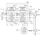
- FIGS. 1 through 8 are circuit diagrams schematically showing an inverter according to first to seventh embodiments of the present invention.
- FIG. 9 is a voltage waveform diagram showing electrical characteristics of the inverter according to the embodiment of the present invention.
- FIGS. 1 through 8 are circuit diagrams schematically showing an inverter according to first to seventh embodiments of the present invention.
- an inverter 100 may include a high voltage gate driving circuit unit 110 , a low voltage gate driving unit 120 , and an inverter unit 130 .
- the high voltage gate driving circuit 110 may include a high voltage gate driving unit 111 , a power supplying unit 112 , and a voltage-dividing unit 113 .
- the high voltage gate driving unit 111 may include a plurality of high voltage gate drivers 111 - 1 to 111 -N. As illustrated in FIG. 1 , first to N-th high voltage gate drivers 111 - 1 to 111 -N may be serially connected between an instruction signal input terminal to which an instruction signal Sa requesting a switching control of the inverter unit 130 is input and a control signal output terminal from which a control signal Sb controlling a switching of the inverter unit 130 is output. The high voltage gate driving unit 111 may control the switching of the inverter unit 130 .
- the instruction signal Sa when the instruction signal Sa is input to the first high voltage gate driver 111 - 1 , information about the switching control included in the instruction signal Sa is transferred to a high voltage gate driver of a rear stage and an N-th high voltage gate driver 111 -N of the last stage transfers the control signal Sb corresponding to an intention of the switching control requested by the instruction signal Sa input to the first high voltage gate driver 111 - 1 to the inverter unit 130 , whereby the switching of the inverter unit 130 may be controlled.
- the inverter unit 130 may switch input power VDC to output AC power and may include at least one inverter arm 131 having at least one high side switch HM and at least one low side switch LM connected to each other in series between an input power terminal to which the input power VDC is input and a ground.
- a plurality high side switches may be connected to each other in series and similarly a plurality of low side switches may be connected to each other in series.
- a gate of the high side switch HM may receive the control signal Sb from the high voltage gate driving unit 111 to thereby control the switching on and switching off and a gate of the low side switch LM may also receive the control signal from the low voltage gate driving unit 120 to thereby control the switching on and switching off, and power having a voltage level corresponding to the input power VDC may be applied to the high voltage gate driving unit 110 according to the switching on and switching off of the high side switch HM.
- the high voltage gate driving circuit unit 110 may include the voltage-dividing unit 113 so that the voltage level of the applied power may be divided and applied to the first to N-th high voltage gate drivers 111 - 1 to 111 -N.
- the voltage-dividing unit 113 may include first to N-th balancers 113 - 1 to 113 -N, and the first to N-th balancers 113 - 1 to 113 -N may correspond to the first to N-th high voltage gate drivers 111 - 1 to 111 -N in a one-to-one scheme to thereby be connected to the corresponding high voltage gate drivers in parallel. Therefore, the first to N-th balancers 113 - 1 to 113 -N may equally divide the voltage level of the power applied to the first to N-th high voltage gate drivers 111 - 1 to 111 -N according to the switching on and switching off of the high side switch HM.
- the input power VDC having a voltage level of 1200V or more is input and the voltage level of the applied power is equally divided according to the switching on and switching off of the high side switch HM.
- two high voltage gate drivers 311 - 1 and 311 - 2 each having a withstand-voltage of 600V are connected to each other in series, or although not illustrated, three high voltage gate drivers each having a withstand-voltage of 400V are connected to each other in series. In this manner, such configuration may replace a relatively expensive high voltage gate driver of 1200V, whereby manufacturing costs may be decreased.
- a voltage-dividing unit 313 may include first and second balancers 313 - 1 and 313 - 2 corresponding to the first and second high voltage gate drivers 311 - 1 and 311 - 2 .
- the first and second balancers 313 - 1 and 313 - 2 may include at least one of resistors R 1 and R 2 connected to each other in series and connected to first and second high voltage gate drivers 611 - 1 , 611 - 2 , 711 - 1 , 711 - 2 , 811 - 1 , and 811 - 2 in parallel or may include at least one of resistors R 1 and R 2 and at least one of diodes D 1 and D 2 connected to the at least one of resistors R 1 and R 2 in parallel.
- the high voltage gate driving unit 111 may have a single power Vcc applied thereto.
- the high voltage driving circuit 110 may further include the power supplying unit 112 .
- the power supplying unit 112 may include a plurality of power suppliers 112 - 1 to 112 -N, and the plurality of power suppliers 112 - 1 to 112 -N may transfer a single power Vcc to the first to N-th high voltage gate drivers 111 - 1 to 111 -N, respectively, to thereby stably supply necessary power to the first to N-th high voltage gate drivers 111 - 1 to 111 -N and have a simple circuit configuration compared with a circuit supplying independent driving powers to the first to N-th high voltage gate drivers 111 - 1 to 111 -N, respectively, whereby manufacturing costs may be further decreased.
- the inverter 300 may include first and second power suppliers 312 - 1 and 312 - 2 corresponding to the first and second high voltage gate drivers 311 - 1 and 311 - 2 , and as in the case of inverters 400 and 500 according to fourth and fifth embodiments of the present invention illustrated in FIGS.
- the first and second power suppliers 312 - 1 and 312 - 2 may include diodes Da and Db, and the diodes Da and Db may be connected to each other in series and connected to first and second high voltage gate drivers 411 - 1 and 411 - 2 in parallel, respectively, or the diodes Da and Db may be connected to each other in parallel and connected to first and second high voltage gate drivers 511 - 1 and 511 - 2 in parallel, respectively.
- the inverter unit 130 may include at least one inverter arm 131 .
- the inverter unit 130 may include one inverter arm 131 .
- an inverter unit 250 may include three inverter arms 251 , 252 , and 253 . Therefore, an inverter 200 according to a second embodiment of the present invention illustrated in FIG.
- first, second, and third high voltage gate driving circuit units 210 , 220 , and 230 controlling the switching on and switching off of high side switches HM 1 , HM 2 , and HM 3 of the three inverter arms 251 , 252 , and 253 .
- the switching on and switching off of low side switches LM 1 , LM 2 , and LM 3 may be controlled by a low voltage gate driving unit 240 .
- the configurations of the first to third high voltage gate driving circuit units 210 , 220 , and 230 are the same as the configuration of the high voltage gate driving circuit unit 110 illustrated in FIG. 1 , the detailed description thereof will be omitted.
- FIG. 9 is a voltage waveform diagram showing electrical characteristics of the inverter according to the embodiment of the present invention.
- the voltage level of power applied according to the switching on and switching off of the high side switch HM may be equally divided by 600V and applied to the high voltage gate drivers 311 - 1 and 311 - 2 , respectively, to thereby employ the high voltage gate drivers each having a withstand-voltage of 600V in the inverter having the input power of 1200V.
- a plurality of driving circuits having the withstand-voltage characteristics lower than 1200V are connected to each other in series and the voltage applied to the plurality of driving circuits at the time of switching is divided to allow the driving circuits to be stably operated, such that a relatively expensive driving circuit having a withstand-voltage of 1200V may be replaced by the driving circuits, whereby manufacturing costs may be decreased.
- a single power is supplied to the plurality of driving circuits, whereby the circuit configuration may be simplified and the manufacturing costs may be further decreased.
Landscapes
- Engineering & Computer Science (AREA)
- Power Engineering (AREA)
- Inverter Devices (AREA)
- Power Conversion In General (AREA)
Abstract
Description
Claims (24)
Applications Claiming Priority (2)
| Application Number | Priority Date | Filing Date | Title |
|---|---|---|---|
| KR10-2012-0107730 | 2012-09-27 | ||
| KR1020120107730A KR101422922B1 (en) | 2012-09-27 | 2012-09-27 | Gate driving circuit and inverter circuit having the same |
Publications (2)
| Publication Number | Publication Date |
|---|---|
| US20140084693A1 US20140084693A1 (en) | 2014-03-27 |
| US9312787B2 true US9312787B2 (en) | 2016-04-12 |
Family
ID=47997306
Family Applications (1)
| Application Number | Title | Priority Date | Filing Date |
|---|---|---|---|
| US13/770,882 Expired - Fee Related US9312787B2 (en) | 2012-09-27 | 2013-02-19 | Inverter with series connected gate driving circuits and voltage divider |
Country Status (5)
| Country | Link |
|---|---|
| US (1) | US9312787B2 (en) |
| EP (1) | EP2713496B1 (en) |
| JP (1) | JP5646665B2 (en) |
| KR (1) | KR101422922B1 (en) |
| CN (1) | CN103701340B (en) |
Cited By (1)
| Publication number | Priority date | Publication date | Assignee | Title |
|---|---|---|---|---|
| US20190229606A1 (en) * | 2017-04-07 | 2019-07-25 | Fujitsu Limited | Gate driving circuit and power supply circuit |
Families Citing this family (1)
| Publication number | Priority date | Publication date | Assignee | Title |
|---|---|---|---|---|
| KR101477377B1 (en) * | 2013-03-20 | 2014-12-29 | 삼성전기주식회사 | Gate driving device and inverter having the same |
Citations (12)
| Publication number | Priority date | Publication date | Assignee | Title |
|---|---|---|---|---|
| US4791345A (en) * | 1986-08-20 | 1988-12-13 | Lgz Landis & Gyr Zug Ag | Driving device for a stepping motor |
| US5212630A (en) * | 1990-12-19 | 1993-05-18 | Mitsubishi Denki Kabushiki Kaisha | Parallel inverter system |
| US5847536A (en) * | 1992-07-03 | 1998-12-08 | Kabushiki Kaisha Toshiba | Motor control circuit equipped with correction means therein |
| JP2000010523A (en) | 1998-06-19 | 2000-01-14 | Denso Corp | Load driving device |
| US6404655B1 (en) * | 1999-12-07 | 2002-06-11 | Semikron, Inc. | Transformerless 3 phase power inverter |
| US20020110008A1 (en) | 2000-01-31 | 2002-08-15 | Hideki Miyazaki | Method and apparatus for driving a semiconductor element with variable resistance circuitry |
| US20040120170A1 (en) * | 2001-12-17 | 2004-06-24 | Coolit Systems Inc. | Inverter |
| KR20050052339A (en) | 2003-11-28 | 2005-06-02 | 미쓰비시덴키 가부시키가이샤 | Inverter circuit |
| JP2007236134A (en) | 2006-03-02 | 2007-09-13 | Tokyo Electric Power Co Inc:The | Semiconductor device gate power supply device |
| CN102069842A (en) | 2009-11-16 | 2011-05-25 | 株式会社捷太格特 | Motor control device, electric power steering system, and vehicle steering system |
| KR20110096713A (en) | 2010-02-23 | 2011-08-31 | 주식회사 다윈전자 | 12 switch integrated intelligent power module |
| US8451045B2 (en) * | 2010-09-17 | 2013-05-28 | Hyundai Motor Company | Inverter control system |
Family Cites Families (4)
| Publication number | Priority date | Publication date | Assignee | Title |
|---|---|---|---|---|
| US5229927A (en) * | 1992-05-15 | 1993-07-20 | Vila Masot Oscar | Self-symmetrizing and self-oscillating half-bridge power inverter |
| KR20040033744A (en) * | 2002-10-15 | 2004-04-28 | 주식회사 하이닉스반도체 | Variable voltage dividing circuit |
| JP2011082764A (en) * | 2009-10-06 | 2011-04-21 | Mitsubishi Electric Corp | Power device control circuit and ipm using the power device control circuit |
| JP5433608B2 (en) * | 2011-03-03 | 2014-03-05 | 日立オートモティブシステムズ株式会社 | Power converter |
-
2012
- 2012-09-27 KR KR1020120107730A patent/KR101422922B1/en not_active Expired - Fee Related
-
2013
- 2013-02-15 JP JP2013027882A patent/JP5646665B2/en not_active Expired - Fee Related
- 2013-02-19 US US13/770,882 patent/US9312787B2/en not_active Expired - Fee Related
- 2013-03-01 CN CN201310066014.9A patent/CN103701340B/en not_active Expired - Fee Related
- 2013-03-26 EP EP13275080.3A patent/EP2713496B1/en not_active Not-in-force
Patent Citations (14)
| Publication number | Priority date | Publication date | Assignee | Title |
|---|---|---|---|---|
| US4791345A (en) * | 1986-08-20 | 1988-12-13 | Lgz Landis & Gyr Zug Ag | Driving device for a stepping motor |
| US5212630A (en) * | 1990-12-19 | 1993-05-18 | Mitsubishi Denki Kabushiki Kaisha | Parallel inverter system |
| US5847536A (en) * | 1992-07-03 | 1998-12-08 | Kabushiki Kaisha Toshiba | Motor control circuit equipped with correction means therein |
| JP2000010523A (en) | 1998-06-19 | 2000-01-14 | Denso Corp | Load driving device |
| US6404655B1 (en) * | 1999-12-07 | 2002-06-11 | Semikron, Inc. | Transformerless 3 phase power inverter |
| US20020110008A1 (en) | 2000-01-31 | 2002-08-15 | Hideki Miyazaki | Method and apparatus for driving a semiconductor element with variable resistance circuitry |
| US20040120170A1 (en) * | 2001-12-17 | 2004-06-24 | Coolit Systems Inc. | Inverter |
| KR20050052339A (en) | 2003-11-28 | 2005-06-02 | 미쓰비시덴키 가부시키가이샤 | Inverter circuit |
| US20090180228A1 (en) | 2003-11-28 | 2009-07-16 | Mitsubishi Denki Kabushiki Kaisha | Inverter circuit |
| JP2007236134A (en) | 2006-03-02 | 2007-09-13 | Tokyo Electric Power Co Inc:The | Semiconductor device gate power supply device |
| CN102069842A (en) | 2009-11-16 | 2011-05-25 | 株式会社捷太格特 | Motor control device, electric power steering system, and vehicle steering system |
| US8525451B2 (en) | 2009-11-16 | 2013-09-03 | Jtekt Corporation | Motor control device, electric power steering system, and vehicle steering system |
| KR20110096713A (en) | 2010-02-23 | 2011-08-31 | 주식회사 다윈전자 | 12 switch integrated intelligent power module |
| US8451045B2 (en) * | 2010-09-17 | 2013-05-28 | Hyundai Motor Company | Inverter control system |
Non-Patent Citations (2)
| Title |
|---|
| Chinese Notification of the First Office Action issued in corresponding Chinese Patent Application No. 2013100660149, mailed on Jul. 10, 2015; with English translation. |
| Office Action issued on Feb. 18, 2014 in the corresponding Japanese Patent Application No. 2013-027882. |
Cited By (2)
| Publication number | Priority date | Publication date | Assignee | Title |
|---|---|---|---|---|
| US20190229606A1 (en) * | 2017-04-07 | 2019-07-25 | Fujitsu Limited | Gate driving circuit and power supply circuit |
| US10715026B2 (en) * | 2017-04-07 | 2020-07-14 | Fujitsu Limited | Gate driving circuit and power supply circuit |
Also Published As
| Publication number | Publication date |
|---|---|
| US20140084693A1 (en) | 2014-03-27 |
| EP2713496B1 (en) | 2019-02-06 |
| KR101422922B1 (en) | 2014-07-23 |
| CN103701340B (en) | 2017-05-10 |
| KR20140040984A (en) | 2014-04-04 |
| EP2713496A3 (en) | 2018-01-24 |
| JP2014073071A (en) | 2014-04-21 |
| CN103701340A (en) | 2014-04-02 |
| JP5646665B2 (en) | 2014-12-24 |
| EP2713496A2 (en) | 2014-04-02 |
Similar Documents
| Publication | Publication Date | Title |
|---|---|---|
| US9294007B2 (en) | Gate driving circuit and inverter having the same | |
| US8649197B2 (en) | Multilevel inverter | |
| US8441818B2 (en) | Method and device for optimizing a space vector pulse width modulation | |
| JP2018133876A (en) | Switching element drive circuit of three-level neutral point clamped type inverter | |
| JP5346749B2 (en) | Power converter | |
| US9425787B2 (en) | Gate driving device and inverter having the same | |
| US9312787B2 (en) | Inverter with series connected gate driving circuits and voltage divider | |
| JP4626259B2 (en) | Power converter control method | |
| CN110752739B (en) | Power equipment driving device | |
| US9130452B2 (en) | Gate driving device including plurality of gate drivers supplied with equally divided voltage and inverter having the same | |
| JP6658135B2 (en) | Multi-level power converter | |
| US10517148B2 (en) | Induction heat cooking apparatus and method for driving the same | |
| US20150145586A1 (en) | Gate driving device and inverter having the same | |
| JP7040125B2 (en) | Drive circuit of the switch to be driven | |
| KR20140072543A (en) | Gate driving device and inverter having the same | |
| US9178516B1 (en) | Voltage-level shift apparatus and method of operating the same | |
| KR100984011B1 (en) | Series-Parallel Driver Circuit Apparatus and Method for Constructing Series-Parallel Driver Circuit | |
| KR20180110557A (en) | Modular Multilevel Converter | |
| JP2017055497A (en) | Gate drive circuit | |
| JP2015220778A (en) | Motor controller and motor control system | |
| JP2021083262A (en) | Inverter device | |
| KR20170001915A (en) | Electronic motor system | |
| KR20150145001A (en) | Gate driving device and inverter having the same | |
| JP2016127695A (en) | Motor drive device and power steering device | |
| RU2009105250A (en) | REGULATED VOLTAGE SUPPLY SYSTEM |
Legal Events
| Date | Code | Title | Description |
|---|---|---|---|
| AS | Assignment |
Owner name: SANSUNG ELECTRO-MECHANICS CO., LTD., KOREA, REPUBL Free format text: ASSIGNMENT OF ASSIGNORS INTEREST;ASSIGNORS:JEONG, IN WHA;SUH, BUM SEOK;REEL/FRAME:030069/0827 Effective date: 20130114 |
|
| AS | Assignment |
Owner name: SAMSUNG ELECTRO-MECHANICS CO., LTD., KOREA, REPUBL Free format text: CORRECTIVE ASSIGNMENT TO CORRECT THE ASSIGNEE PREVIOUSLY RECORDED ON REEL 030069 FRAME 0827. ASSIGNOR(S) HEREBY CONFIRMS THE ASSIGNEE SHOULD READ AS SAMSUNG ELECTRO-MECHANICS CO., LTD.;ASSIGNORS:JEONG, IN WHA;SUH, BUM SEOK;REEL/FRAME:034504/0070 Effective date: 20130114 |
|
| FEPP | Fee payment procedure |
Free format text: PAYOR NUMBER ASSIGNED (ORIGINAL EVENT CODE: ASPN); ENTITY STATUS OF PATENT OWNER: LARGE ENTITY |
|
| STCF | Information on status: patent grant |
Free format text: PATENTED CASE |
|
| MAFP | Maintenance fee payment |
Free format text: PAYMENT OF MAINTENANCE FEE, 4TH YEAR, LARGE ENTITY (ORIGINAL EVENT CODE: M1551); ENTITY STATUS OF PATENT OWNER: LARGE ENTITY Year of fee payment: 4 |
|
| FEPP | Fee payment procedure |
Free format text: MAINTENANCE FEE REMINDER MAILED (ORIGINAL EVENT CODE: REM.); ENTITY STATUS OF PATENT OWNER: LARGE ENTITY |
|
| LAPS | Lapse for failure to pay maintenance fees |
Free format text: PATENT EXPIRED FOR FAILURE TO PAY MAINTENANCE FEES (ORIGINAL EVENT CODE: EXP.); ENTITY STATUS OF PATENT OWNER: LARGE ENTITY |
|
| STCH | Information on status: patent discontinuation |
Free format text: PATENT EXPIRED DUE TO NONPAYMENT OF MAINTENANCE FEES UNDER 37 CFR 1.362 |
|
| FP | Lapsed due to failure to pay maintenance fee |
Effective date: 20240412 |