US9312357B1 - Semiconductor device and method for manufacturing the same - Google Patents
Semiconductor device and method for manufacturing the same Download PDFInfo
- Publication number
- US9312357B1 US9312357B1 US14/515,514 US201414515514A US9312357B1 US 9312357 B1 US9312357 B1 US 9312357B1 US 201414515514 A US201414515514 A US 201414515514A US 9312357 B1 US9312357 B1 US 9312357B1
- Authority
- US
- United States
- Prior art keywords
- layer
- dielectric layer
- gate
- metal layer
- semiconductor device
- Prior art date
- Legal status (The legal status is an assumption and is not a legal conclusion. Google has not performed a legal analysis and makes no representation as to the accuracy of the status listed.)
- Active
Links
Images


Classifications
-
- H01L29/511—
-
- H—ELECTRICITY
- H10—SEMICONDUCTOR DEVICES; ELECTRIC SOLID-STATE DEVICES NOT OTHERWISE PROVIDED FOR
- H10D—INORGANIC ELECTRIC SEMICONDUCTOR DEVICES
- H10D64/00—Electrodes of devices having potential barriers
- H10D64/60—Electrodes characterised by their materials
- H10D64/66—Electrodes having a conductor capacitively coupled to a semiconductor by an insulator, e.g. MIS electrodes
- H10D64/68—Electrodes having a conductor capacitively coupled to a semiconductor by an insulator, e.g. MIS electrodes characterised by the insulator, e.g. by the gate insulator
- H10D64/681—Electrodes having a conductor capacitively coupled to a semiconductor by an insulator, e.g. MIS electrodes characterised by the insulator, e.g. by the gate insulator having a compositional variation, e.g. multilayered
-
- H—ELECTRICITY
- H01—ELECTRIC ELEMENTS
- H01L—SEMICONDUCTOR DEVICES NOT COVERED BY CLASS H10
- H01L21/00—Processes or apparatus adapted for the manufacture or treatment of semiconductor or solid state devices or of parts thereof
- H01L21/02—Manufacture or treatment of semiconductor devices or of parts thereof
- H01L21/02104—Forming layers
- H01L21/02107—Forming insulating materials on a substrate
- H01L21/02109—Forming insulating materials on a substrate characterised by the type of layer, e.g. type of material, porous/non-porous, pre-cursors, mixtures or laminates
- H01L21/02112—Forming insulating materials on a substrate characterised by the type of layer, e.g. type of material, porous/non-porous, pre-cursors, mixtures or laminates characterised by the material of the layer
- H01L21/02172—Forming insulating materials on a substrate characterised by the type of layer, e.g. type of material, porous/non-porous, pre-cursors, mixtures or laminates characterised by the material of the layer the material containing at least one metal element, e.g. metal oxides, metal nitrides, metal oxynitrides or metal carbides
- H01L21/02175—Forming insulating materials on a substrate characterised by the type of layer, e.g. type of material, porous/non-porous, pre-cursors, mixtures or laminates characterised by the material of the layer the material containing at least one metal element, e.g. metal oxides, metal nitrides, metal oxynitrides or metal carbides characterised by the metal
- H01L21/02178—Forming insulating materials on a substrate characterised by the type of layer, e.g. type of material, porous/non-porous, pre-cursors, mixtures or laminates characterised by the material of the layer the material containing at least one metal element, e.g. metal oxides, metal nitrides, metal oxynitrides or metal carbides characterised by the metal the material containing aluminium, e.g. Al2O3
-
- H—ELECTRICITY
- H01—ELECTRIC ELEMENTS
- H01L—SEMICONDUCTOR DEVICES NOT COVERED BY CLASS H10
- H01L21/00—Processes or apparatus adapted for the manufacture or treatment of semiconductor or solid state devices or of parts thereof
- H01L21/02—Manufacture or treatment of semiconductor devices or of parts thereof
- H01L21/02104—Forming layers
- H01L21/02107—Forming insulating materials on a substrate
- H01L21/02225—Forming insulating materials on a substrate characterised by the process for the formation of the insulating layer
- H01L21/02227—Forming insulating materials on a substrate characterised by the process for the formation of the insulating layer formation by a process other than a deposition process
- H01L21/0223—Forming insulating materials on a substrate characterised by the process for the formation of the insulating layer formation by a process other than a deposition process formation by oxidation, e.g. oxidation of the substrate
- H01L21/02244—Forming insulating materials on a substrate characterised by the process for the formation of the insulating layer formation by a process other than a deposition process formation by oxidation, e.g. oxidation of the substrate of a metallic layer
-
- H—ELECTRICITY
- H01—ELECTRIC ELEMENTS
- H01L—SEMICONDUCTOR DEVICES NOT COVERED BY CLASS H10
- H01L21/00—Processes or apparatus adapted for the manufacture or treatment of semiconductor or solid state devices or of parts thereof
- H01L21/02—Manufacture or treatment of semiconductor devices or of parts thereof
- H01L21/02104—Forming layers
- H01L21/02107—Forming insulating materials on a substrate
- H01L21/02225—Forming insulating materials on a substrate characterised by the process for the formation of the insulating layer
- H01L21/02227—Forming insulating materials on a substrate characterised by the process for the formation of the insulating layer formation by a process other than a deposition process
- H01L21/02247—Forming insulating materials on a substrate characterised by the process for the formation of the insulating layer formation by a process other than a deposition process formation by nitridation, e.g. nitridation of the substrate
-
- H—ELECTRICITY
- H01—ELECTRIC ELEMENTS
- H01L—SEMICONDUCTOR DEVICES NOT COVERED BY CLASS H10
- H01L21/00—Processes or apparatus adapted for the manufacture or treatment of semiconductor or solid state devices or of parts thereof
- H01L21/02—Manufacture or treatment of semiconductor devices or of parts thereof
- H01L21/04—Manufacture or treatment of semiconductor devices or of parts thereof the devices having potential barriers, e.g. a PN junction, depletion layer or carrier concentration layer
- H01L21/18—Manufacture or treatment of semiconductor devices or of parts thereof the devices having potential barriers, e.g. a PN junction, depletion layer or carrier concentration layer the devices having semiconductor bodies comprising elements of Group IV of the Periodic Table or AIIIBV compounds with or without impurities, e.g. doping materials
- H01L21/28—Manufacture of electrodes on semiconductor bodies using processes or apparatus not provided for in groups H01L21/20 - H01L21/268
- H01L21/28008—Making conductor-insulator-semiconductor electrodes
- H01L21/28017—Making conductor-insulator-semiconductor electrodes the insulator being formed after the semiconductor body, the semiconductor being silicon
- H01L21/28026—Making conductor-insulator-semiconductor electrodes the insulator being formed after the semiconductor body, the semiconductor being silicon characterised by the conductor
- H01L21/28079—Making conductor-insulator-semiconductor electrodes the insulator being formed after the semiconductor body, the semiconductor being silicon characterised by the conductor the final conductor layer next to the insulator being a single metal, e.g. Ta, W, Mo, Al
-
- H—ELECTRICITY
- H01—ELECTRIC ELEMENTS
- H01L—SEMICONDUCTOR DEVICES NOT COVERED BY CLASS H10
- H01L21/00—Processes or apparatus adapted for the manufacture or treatment of semiconductor or solid state devices or of parts thereof
- H01L21/02—Manufacture or treatment of semiconductor devices or of parts thereof
- H01L21/04—Manufacture or treatment of semiconductor devices or of parts thereof the devices having potential barriers, e.g. a PN junction, depletion layer or carrier concentration layer
- H01L21/18—Manufacture or treatment of semiconductor devices or of parts thereof the devices having potential barriers, e.g. a PN junction, depletion layer or carrier concentration layer the devices having semiconductor bodies comprising elements of Group IV of the Periodic Table or AIIIBV compounds with or without impurities, e.g. doping materials
- H01L21/28—Manufacture of electrodes on semiconductor bodies using processes or apparatus not provided for in groups H01L21/20 - H01L21/268
- H01L21/28008—Making conductor-insulator-semiconductor electrodes
- H01L21/28017—Making conductor-insulator-semiconductor electrodes the insulator being formed after the semiconductor body, the semiconductor being silicon
- H01L21/28158—Making the insulator
-
- H—ELECTRICITY
- H01—ELECTRIC ELEMENTS
- H01L—SEMICONDUCTOR DEVICES NOT COVERED BY CLASS H10
- H01L21/00—Processes or apparatus adapted for the manufacture or treatment of semiconductor or solid state devices or of parts thereof
- H01L21/02—Manufacture or treatment of semiconductor devices or of parts thereof
- H01L21/04—Manufacture or treatment of semiconductor devices or of parts thereof the devices having potential barriers, e.g. a PN junction, depletion layer or carrier concentration layer
- H01L21/18—Manufacture or treatment of semiconductor devices or of parts thereof the devices having potential barriers, e.g. a PN junction, depletion layer or carrier concentration layer the devices having semiconductor bodies comprising elements of Group IV of the Periodic Table or AIIIBV compounds with or without impurities, e.g. doping materials
- H01L21/30—Treatment of semiconductor bodies using processes or apparatus not provided for in groups H01L21/20 - H01L21/26
- H01L21/31—Treatment of semiconductor bodies using processes or apparatus not provided for in groups H01L21/20 - H01L21/26 to form insulating layers thereon, e.g. for masking or by using photolithographic techniques; After treatment of these layers; Selection of materials for these layers
- H01L21/3205—Deposition of non-insulating-, e.g. conductive- or resistive-, layers on insulating layers; After-treatment of these layers
- H01L21/321—After treatment
- H01L21/32115—Planarisation
- H01L21/3212—Planarisation by chemical mechanical polishing [CMP]
-
- H—ELECTRICITY
- H01—ELECTRIC ELEMENTS
- H01L—SEMICONDUCTOR DEVICES NOT COVERED BY CLASS H10
- H01L21/00—Processes or apparatus adapted for the manufacture or treatment of semiconductor or solid state devices or of parts thereof
- H01L21/70—Manufacture or treatment of devices consisting of a plurality of solid state components formed in or on a common substrate or of parts thereof; Manufacture of integrated circuit devices or of parts thereof
- H01L21/71—Manufacture of specific parts of devices defined in group H01L21/70
- H01L21/768—Applying interconnections to be used for carrying current between separate components within a device comprising conductors and dielectrics
- H01L21/76897—Formation of self-aligned vias or contact plugs, i.e. involving a lithographically uncritical step
-
- H01L29/42364—
-
- H01L29/495—
-
- H—ELECTRICITY
- H10—SEMICONDUCTOR DEVICES; ELECTRIC SOLID-STATE DEVICES NOT OTHERWISE PROVIDED FOR
- H10D—INORGANIC ELECTRIC SEMICONDUCTOR DEVICES
- H10D30/00—Field-effect transistors [FET]
- H10D30/60—Insulated-gate field-effect transistors [IGFET]
- H10D30/791—Arrangements for exerting mechanical stress on the crystal lattice of the channel regions
- H10D30/797—Arrangements for exerting mechanical stress on the crystal lattice of the channel regions being in source or drain regions, e.g. SiGe source or drain
-
- H10D64/01316—
-
- H10D64/01318—
-
- H10D64/01332—
-
- H—ELECTRICITY
- H10—SEMICONDUCTOR DEVICES; ELECTRIC SOLID-STATE DEVICES NOT OTHERWISE PROVIDED FOR
- H10D—INORGANIC ELECTRIC SEMICONDUCTOR DEVICES
- H10D64/00—Electrodes of devices having potential barriers
- H10D64/01—Manufacture or treatment
- H10D64/017—Manufacture or treatment using dummy gates in processes wherein at least parts of the final gates are self-aligned to the dummy gates, i.e. replacement gate processes
-
- H—ELECTRICITY
- H10—SEMICONDUCTOR DEVICES; ELECTRIC SOLID-STATE DEVICES NOT OTHERWISE PROVIDED FOR
- H10D—INORGANIC ELECTRIC SEMICONDUCTOR DEVICES
- H10D64/00—Electrodes of devices having potential barriers
- H10D64/20—Electrodes characterised by their shapes, relative sizes or dispositions
- H10D64/27—Electrodes not carrying the current to be rectified, amplified, oscillated or switched, e.g. gates
- H10D64/311—Gate electrodes for field-effect devices
- H10D64/411—Gate electrodes for field-effect devices for FETs
- H10D64/511—Gate electrodes for field-effect devices for FETs for IGFETs
- H10D64/514—Gate electrodes for field-effect devices for FETs for IGFETs characterised by the insulating layers
-
- H—ELECTRICITY
- H10—SEMICONDUCTOR DEVICES; ELECTRIC SOLID-STATE DEVICES NOT OTHERWISE PROVIDED FOR
- H10D—INORGANIC ELECTRIC SEMICONDUCTOR DEVICES
- H10D64/00—Electrodes of devices having potential barriers
- H10D64/60—Electrodes characterised by their materials
- H10D64/66—Electrodes having a conductor capacitively coupled to a semiconductor by an insulator, e.g. MIS electrodes
- H10D64/665—Electrodes having a conductor capacitively coupled to a semiconductor by an insulator, e.g. MIS electrodes the conductor comprising a layer of elemental metal contacting the insulator, e.g. tungsten or molybdenum
-
- H—ELECTRICITY
- H10—SEMICONDUCTOR DEVICES; ELECTRIC SOLID-STATE DEVICES NOT OTHERWISE PROVIDED FOR
- H10D—INORGANIC ELECTRIC SEMICONDUCTOR DEVICES
- H10D64/00—Electrodes of devices having potential barriers
- H10D64/60—Electrodes characterised by their materials
- H10D64/66—Electrodes having a conductor capacitively coupled to a semiconductor by an insulator, e.g. MIS electrodes
- H10D64/667—Electrodes having a conductor capacitively coupled to a semiconductor by an insulator, e.g. MIS electrodes the conductor comprising a layer of alloy material, compound material or organic material contacting the insulator, e.g. TiN workfunction layers
-
- H10P14/6939—
-
- H10P14/69391—
-
- H10P52/403—
-
- H10W20/069—
-
- H—ELECTRICITY
- H01—ELECTRIC ELEMENTS
- H01L—SEMICONDUCTOR DEVICES NOT COVERED BY CLASS H10
- H01L21/00—Processes or apparatus adapted for the manufacture or treatment of semiconductor or solid state devices or of parts thereof
- H01L21/02—Manufacture or treatment of semiconductor devices or of parts thereof
- H01L21/02104—Forming layers
- H01L21/02107—Forming insulating materials on a substrate
- H01L21/02225—Forming insulating materials on a substrate characterised by the process for the formation of the insulating layer
- H01L21/02227—Forming insulating materials on a substrate characterised by the process for the formation of the insulating layer formation by a process other than a deposition process
- H01L21/02252—Forming insulating materials on a substrate characterised by the process for the formation of the insulating layer formation by a process other than a deposition process formation by plasma treatment, e.g. plasma oxidation of the substrate
-
- H—ELECTRICITY
- H10—SEMICONDUCTOR DEVICES; ELECTRIC SOLID-STATE DEVICES NOT OTHERWISE PROVIDED FOR
- H10D—INORGANIC ELECTRIC SEMICONDUCTOR DEVICES
- H10D30/00—Field-effect transistors [FET]
- H10D30/01—Manufacture or treatment
- H10D30/021—Manufacture or treatment of FETs having insulated gates [IGFET]
- H10D30/027—Manufacture or treatment of FETs having insulated gates [IGFET] of lateral single-gate IGFETs
- H10D30/0275—Manufacture or treatment of FETs having insulated gates [IGFET] of lateral single-gate IGFETs forming single crystalline semiconductor source or drain regions resulting in recessed gates, e.g. forming raised source or drain regions
-
- H—ELECTRICITY
- H10—SEMICONDUCTOR DEVICES; ELECTRIC SOLID-STATE DEVICES NOT OTHERWISE PROVIDED FOR
- H10D—INORGANIC ELECTRIC SEMICONDUCTOR DEVICES
- H10D62/00—Semiconductor bodies, or regions thereof, of devices having potential barriers
- H10D62/01—Manufacture or treatment
- H10D62/021—Forming source or drain recesses by etching e.g. recessing by etching and then refilling
-
- H—ELECTRICITY
- H10—SEMICONDUCTOR DEVICES; ELECTRIC SOLID-STATE DEVICES NOT OTHERWISE PROVIDED FOR
- H10D—INORGANIC ELECTRIC SEMICONDUCTOR DEVICES
- H10D64/00—Electrodes of devices having potential barriers
- H10D64/60—Electrodes characterised by their materials
- H10D64/66—Electrodes having a conductor capacitively coupled to a semiconductor by an insulator, e.g. MIS electrodes
- H10D64/68—Electrodes having a conductor capacitively coupled to a semiconductor by an insulator, e.g. MIS electrodes characterised by the insulator, e.g. by the gate insulator
- H10D64/681—Electrodes having a conductor capacitively coupled to a semiconductor by an insulator, e.g. MIS electrodes characterised by the insulator, e.g. by the gate insulator having a compositional variation, e.g. multilayered
- H10D64/685—Electrodes having a conductor capacitively coupled to a semiconductor by an insulator, e.g. MIS electrodes characterised by the insulator, e.g. by the gate insulator having a compositional variation, e.g. multilayered being perpendicular to the channel plane
-
- H—ELECTRICITY
- H10—SEMICONDUCTOR DEVICES; ELECTRIC SOLID-STATE DEVICES NOT OTHERWISE PROVIDED FOR
- H10D—INORGANIC ELECTRIC SEMICONDUCTOR DEVICES
- H10D64/00—Electrodes of devices having potential barriers
- H10D64/60—Electrodes characterised by their materials
- H10D64/66—Electrodes having a conductor capacitively coupled to a semiconductor by an insulator, e.g. MIS electrodes
- H10D64/68—Electrodes having a conductor capacitively coupled to a semiconductor by an insulator, e.g. MIS electrodes characterised by the insulator, e.g. by the gate insulator
- H10D64/693—Electrodes having a conductor capacitively coupled to a semiconductor by an insulator, e.g. MIS electrodes characterised by the insulator, e.g. by the gate insulator the insulator comprising nitrogen, e.g. nitrides, oxynitrides or nitrogen-doped materials
-
- H—ELECTRICITY
- H10—SEMICONDUCTOR DEVICES; ELECTRIC SOLID-STATE DEVICES NOT OTHERWISE PROVIDED FOR
- H10D—INORGANIC ELECTRIC SEMICONDUCTOR DEVICES
- H10D84/00—Integrated devices formed in or on semiconductor substrates that comprise only semiconducting layers, e.g. on Si wafers or on GaAs-on-Si wafers
- H10D84/01—Manufacture or treatment
- H10D84/0123—Integrating together multiple components covered by H10D12/00 or H10D30/00, e.g. integrating multiple IGBTs
- H10D84/0126—Integrating together multiple components covered by H10D12/00 or H10D30/00, e.g. integrating multiple IGBTs the components including insulated gates, e.g. IGFETs
- H10D84/0165—Integrating together multiple components covered by H10D12/00 or H10D30/00, e.g. integrating multiple IGBTs the components including insulated gates, e.g. IGFETs the components including complementary IGFETs, e.g. CMOS devices
- H10D84/017—Manufacturing their source or drain regions, e.g. silicided source or drain regions
-
- H—ELECTRICITY
- H10—SEMICONDUCTOR DEVICES; ELECTRIC SOLID-STATE DEVICES NOT OTHERWISE PROVIDED FOR
- H10D—INORGANIC ELECTRIC SEMICONDUCTOR DEVICES
- H10D84/00—Integrated devices formed in or on semiconductor substrates that comprise only semiconducting layers, e.g. on Si wafers or on GaAs-on-Si wafers
- H10D84/01—Manufacture or treatment
- H10D84/0123—Integrating together multiple components covered by H10D12/00 or H10D30/00, e.g. integrating multiple IGBTs
- H10D84/0126—Integrating together multiple components covered by H10D12/00 or H10D30/00, e.g. integrating multiple IGBTs the components including insulated gates, e.g. IGFETs
- H10D84/0165—Integrating together multiple components covered by H10D12/00 or H10D30/00, e.g. integrating multiple IGBTs the components including insulated gates, e.g. IGFETs the components including complementary IGFETs, e.g. CMOS devices
- H10D84/0172—Manufacturing their gate conductors
-
- H—ELECTRICITY
- H10—SEMICONDUCTOR DEVICES; ELECTRIC SOLID-STATE DEVICES NOT OTHERWISE PROVIDED FOR
- H10D—INORGANIC ELECTRIC SEMICONDUCTOR DEVICES
- H10D84/00—Integrated devices formed in or on semiconductor substrates that comprise only semiconducting layers, e.g. on Si wafers or on GaAs-on-Si wafers
- H10D84/01—Manufacture or treatment
- H10D84/02—Manufacture or treatment characterised by using material-based technologies
- H10D84/03—Manufacture or treatment characterised by using material-based technologies using Group IV technology, e.g. silicon technology or silicon-carbide [SiC] technology
- H10D84/038—Manufacture or treatment characterised by using material-based technologies using Group IV technology, e.g. silicon technology or silicon-carbide [SiC] technology using silicon technology, e.g. SiGe
-
- H10P14/6314—
-
- H10P14/6316—
-
- H10P14/6319—
Definitions
- the present invention generally relates to a semiconductor processing technology and, more particularly to, a semiconductor device and a method for manufacturing the same.
- MOSFET metal-oxide-semiconductor field-effect transistors
- the metal gate resistance (R s _ MG ) increases with the thinning of aluminum of the metal gate, which causes the device characteristics to change with the processing parameters of aluminum of the metal gate. For example, for I/O devices with a larger gate area than that of the core devices, dishing due to over-polishing often happens in low pattern density areas (for example, the gate area of an I/O device), during the chemical-mechanical polishing (CMP) planarization process. As a result, the metal gate resistance (R s _ MG ) increases with the thinning of aluminum of the metal gate to enhance the threshold voltage (V) and lower the turn-on current (I on ). Even worse, threshold voltage mismatch occurs for paired I/O devices due to thickness difference between the metal gates when dishing appears. Both of the above lead to chip malfunction.
- the present invention provides a method for manufacturing a semiconductor device.
- the method includes steps hereinafter.
- a substrate is provided with a first dielectric layer thereon.
- the first dielectric layer is provided with a trench.
- a metal layer is formed to fill the trench and to cover the surface of the first dielectric layer.
- the metal layer is partially removed so that a remaining portion of the metal layer covers the first dielectric layer.
- a treatment process is performed to transform the remaining portion of the metal layer into a passivation layer on the top portion and a gate metal layer on the bottom portion.
- a chemical-mechanical polishing process is performed until the first dielectric layer is exposed so that a remaining portion of the passivation layer remains in the trench.
- the present invention further provides a semiconductor device.
- the semiconductor device includes a substrate with a first dielectric layer and a gate structure thereon.
- the gate structure includes a gate dielectric layer, a gate metal layer and a passivation layer from bottom up.
- the passivation layer includes a compound including elements the gate metal layer is formed of.
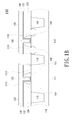
- FIG. 1A to FIG. 1E are cross-sectional views showing steps for a method for manufacturing a semiconductor device according to one embodiment of the present invention.
- FIG. 1A to FIG. 1E cross-sectional views showing steps for a method for manufacturing a semiconductor device 100 according to one embodiment of the present invention.
- a substrate 110 is provided with a first dielectric layer 120 thereon.
- the first dielectric layer 120 includes at least one trench 125 .
- the substrate 110 can be a silicon substrate, a III-V semiconductor substrate, a sapphire substrate, a silicon on insulator (SOI) substrate, or any other substrates with electronic components thereon.
- the substrate 110 is a silicon substrate having at least one n-channel MOSFET 111 and at least one p-channel MOSFET 112 that are separated by a shallow trench isolation (STI) structure 113 therebetween.
- the first dielectric layer 120 is an oxide layer or any other low-k dielectric layers formed by deposition.
- the first dielectric layer 120 can be a carbon-doped oxide layer.
- the (at least one) trench 125 is defined by a sidewall of a spacer 124 .
- the spacer 124 can be formed of, for example, nitride.
- the source/drain regions 1111 of the n-channel MOSFET 111 may include silicon doped with group V elements such as phosphor (P) so that there is provided a tensile strain in the channel between the source/drain regions 1111 to improve electron mobility.
- the source/drain regions 1121 of the p-channel MOSFET 112 may include silicon-germanium (SiGe). The lattice constant of silicon-germanium is larger than that of silicon so that there is provided a compressive strain in the channel between the source/drain regions 1121 to improve hole mobility.
- a second dielectric layer 121 and a stacked layer 122 ( 123 ) are formed in sequence to cover the bottom surface of the trench 125 , the sidewall of the spacer 124 and the top surface of the first dielectric layer 120 .
- the second dielectric layer 121 is a high-k dielectric layer including, for example, hafnium-based dielectric materials, such as HfO 2 and HfSiO, etc.
- the stacked layer 122 ( 123 ) includes a barrier layer and a work function metal layer.
- the barrier layer may include a titanium nitride (TiN) layer and a tantalum nitride (TaN) layer.
- the work function metal layer may include a titanium-aluminum (TiAl) alloy layer.
- the barrier layer may include a titanium nitride (TiN) layer and a tantalum nitride (TaN) layer.
- the work function metal layer may include a two-layered structure including a titanium-aluminum (TiAl) alloy layer on the top and a titanium nitride (TiN) layer at the bottom thereof.
- TiAl titanium-aluminum
- TiN titanium nitride
- the present invention is not limited to the two-layered structure as above. Modifications within the scope of the present invention may be made by those of ordinary skills in the art.
- a metal layer 130 is deposited to fill the trench 125 and cover the surface of the first dielectric layer 120 .
- the metal layer 130 may include Al, W or Cu.
- the present invention is not limited to the material the metal layer 130 is made of. Modifications within the scope of the present invention may be made by those of ordinary skills in the art.
- the metal layer 130 is partially removed so that a remaining portion 131 of the metal layer 130 covers the first dielectric layer 120 .
- the metal layer 130 is partially removed by processes such as etching and chemical-mechanical polishing, etc.
- the thickness of the remaining portion 131 is smaller than 20 nm.
- the remaining portion 131 is thinner than 10 nm.
- a treatment process is performed so that a top portion of the remaining portion 131 of the metal layer 130 is transformed into a passivation layer 132 and a bottom portion of the remaining portion 131 of the metal layer 130 is transformed into a gate metal layer 133 .
- the gate metal layer 133 is bulk-shaped.
- the treatment process is performed by plasma-enhanced oxidation or plasma-enhanced nitridation.
- the passivation layer 132 includes a compound having elements that the gate metal layer 133 is formed of. More particularly, the passivation layer 132 may include metal oxide or metal nitride.
- a chemical-mechanical polishing (CMP) process is performed until the first dielectric layer 120 is exposed so that a remaining portion 134 of the passivation layer 132 remains in the trench 125 .
- CMP chemical-mechanical polishing
- the thickness of the remaining portion 134 of the passivation layer 132 is smaller than 10 nm.
- the thickness of the remaining portion 134 is in a range from 2 nm to 8 nm.
- a contact plug (not shown) is provided penetrating the remaining portion 134 of the passivation layer 132 to connect the gate metal layer 133 .
- the semiconductor device 100 is manufactured, as shown in FIG. 1E .
- the semiconductor device 100 includes a substrate 110 with a first dielectric layer 120 and a gate structure 140 thereon.
- the gate structure 140 includes a gate dielectric layer 126 , a gate metal layer 133 and a (passivation layer) remaining portion 134 from bottom up.
- the passivation layer remaining portion 134 includes a compound including elements that the gate metal layer 133 is formed of.
- the gate structure 140 is defined by the sidewall of the spacer 124 .
- the gate structure 140 may further include a stacked layer 127 ( 128 ) provided between the gate dielectric layer 126 and the gate metal layer 133 .
- the gate dielectric layer 126 and the stacked layer 127 ( 128 ) are U-shaped, and configured along the sidewall of the spacer 124 and the bottom surface of the trench 125 .
- the semiconductor device 100 may further include a contact plug (not shown) penetrating the passivation layer remaining portion 134 to connect the gate metal layer 133 .
- the gate structure in FIG. 1E of the one embodiment of present invention is a high-k last gate structure.
- the present invention is not limited thereto. In other words, the disclosure of the present invention may also be used to manufacture a semiconductor device with a high-k first gate structure.
- the passivation layer 134 of the semiconductor device 100 in FIG. 1E can prevent dishing effects due to over-polishing of the gate area of a semiconductor device. Therefore, the present invention is presented to improve I-V characteristics, avoid threshold voltage mismatch for paired I/O devices, and prevent chip malfunction.
Landscapes
- Engineering & Computer Science (AREA)
- Physics & Mathematics (AREA)
- Condensed Matter Physics & Semiconductors (AREA)
- General Physics & Mathematics (AREA)
- Manufacturing & Machinery (AREA)
- Computer Hardware Design (AREA)
- Microelectronics & Electronic Packaging (AREA)
- Power Engineering (AREA)
- Insulated Gate Type Field-Effect Transistor (AREA)
- Internal Circuitry In Semiconductor Integrated Circuit Devices (AREA)
- Electrodes Of Semiconductors (AREA)
Abstract
Description
Claims (19)
Applications Claiming Priority (3)
| Application Number | Priority Date | Filing Date | Title |
|---|---|---|---|
| CN201410524797.5A CN105529304B (en) | 2014-09-30 | 2014-09-30 | Semiconductor device and method for manufacturing the same |
| CN201410524797.5 | 2014-09-30 | ||
| CN201410524797 | 2014-09-30 |
Publications (2)
| Publication Number | Publication Date |
|---|---|
| US20160093712A1 US20160093712A1 (en) | 2016-03-31 |
| US9312357B1 true US9312357B1 (en) | 2016-04-12 |
Family
ID=55585343
Family Applications (1)
| Application Number | Title | Priority Date | Filing Date |
|---|---|---|---|
| US14/515,514 Active US9312357B1 (en) | 2014-09-30 | 2014-10-16 | Semiconductor device and method for manufacturing the same |
Country Status (2)
| Country | Link |
|---|---|
| US (1) | US9312357B1 (en) |
| CN (1) | CN105529304B (en) |
Families Citing this family (1)
| Publication number | Priority date | Publication date | Assignee | Title |
|---|---|---|---|---|
| CN108630540B (en) * | 2017-03-24 | 2021-05-28 | 中芯国际集成电路制造(上海)有限公司 | Semiconductor device and method of manufacturing the same |
Citations (3)
| Publication number | Priority date | Publication date | Assignee | Title |
|---|---|---|---|---|
| US20020068394A1 (en) * | 2000-12-04 | 2002-06-06 | Nobuaki Tokushige | Semiconductor device and fabrication process therefor |
| US20100213555A1 (en) * | 2009-02-23 | 2010-08-26 | Advanced Micro Devices, Inc. | Metal oxide semiconductor devices having capping layers and methods for fabricating the same |
| US20130043592A1 (en) * | 2011-08-19 | 2013-02-21 | Globalfoundries Inc. | Methods of Forming a Replacement Gate Comprised of Silicon and a Device Including Same |
Family Cites Families (5)
| Publication number | Priority date | Publication date | Assignee | Title |
|---|---|---|---|---|
| US20020192941A1 (en) * | 2001-06-19 | 2002-12-19 | Chia-Lin Hsu | Method for reducing dishing in copper chemical mechanical polishing process |
| US7126199B2 (en) * | 2004-09-27 | 2006-10-24 | Intel Corporation | Multilayer metal gate electrode |
| US8809179B2 (en) * | 2006-04-13 | 2014-08-19 | Taiwan Semiconductor Manufacturing Company, Ltd. | Method for reducing topography of non-volatile memory and resulting memory cells |
| US8704229B2 (en) * | 2011-07-26 | 2014-04-22 | Globalfoundries Inc. | Partial poly amorphization for channeling prevention |
| US8580628B2 (en) * | 2012-02-02 | 2013-11-12 | GlobalFoundries, Inc. | Integrated circuit contact structure and method |
-
2014
- 2014-09-30 CN CN201410524797.5A patent/CN105529304B/en active Active
- 2014-10-16 US US14/515,514 patent/US9312357B1/en active Active
Patent Citations (3)
| Publication number | Priority date | Publication date | Assignee | Title |
|---|---|---|---|---|
| US20020068394A1 (en) * | 2000-12-04 | 2002-06-06 | Nobuaki Tokushige | Semiconductor device and fabrication process therefor |
| US20100213555A1 (en) * | 2009-02-23 | 2010-08-26 | Advanced Micro Devices, Inc. | Metal oxide semiconductor devices having capping layers and methods for fabricating the same |
| US20130043592A1 (en) * | 2011-08-19 | 2013-02-21 | Globalfoundries Inc. | Methods of Forming a Replacement Gate Comprised of Silicon and a Device Including Same |
Also Published As
| Publication number | Publication date |
|---|---|
| CN105529304A (en) | 2016-04-27 |
| CN105529304B (en) | 2019-06-18 |
| US20160093712A1 (en) | 2016-03-31 |
Similar Documents
| Publication | Publication Date | Title |
|---|---|---|
| US9831133B2 (en) | Semiconductor devices having metal gate and method for manufacturing semiconductor devices having metal gate | |
| US8008145B2 (en) | High-K metal gate structure fabrication method including hard mask | |
| US10340272B2 (en) | Manufacturing method of semiconductor device | |
| US9496354B2 (en) | Semiconductor devices with dummy gate structures partially on isolation regions | |
| US9196611B2 (en) | Reduced substrate coupling for inductors in semiconductor devices | |
| CN109994537A (en) | Semiconductor element and preparation method thereof | |
| CN111554578B (en) | Semiconductor structures and methods of forming them | |
| US8691655B2 (en) | Method of semiconductor integrated circuit fabrication | |
| CN110473784B (en) | Semiconductor element and manufacturing method thereof | |
| US9735174B2 (en) | FDSOI—capacitor | |
| US9548317B2 (en) | FDSOI semiconductor structure and method for manufacturing the same | |
| US9378968B2 (en) | Method for planarizing semiconductor device | |
| US11456304B2 (en) | Semiconductor structure and forming method thereof | |
| US11251279B2 (en) | High voltage transistor structure and method of fabricating the same | |
| US9312357B1 (en) | Semiconductor device and method for manufacturing the same | |
| US9472465B2 (en) | Methods of fabricating integrated circuits | |
| US8937006B2 (en) | Method of semiconductor integrated circuit fabrication | |
| US8860151B2 (en) | Semiconductor device having a spacer and a liner overlying a sidewall of a gate structure and method of forming the same | |
| TWI581316B (en) | Method of forming metal silicide layer |
Legal Events
| Date | Code | Title | Description |
|---|---|---|---|
| AS | Assignment |
Owner name: UNITED MICROELECTRONICS CORPORATION, TAIWAN Free format text: ASSIGNMENT OF ASSIGNORS INTEREST;ASSIGNORS:TSAI, SHIH-CHANG;TSENG, TZU-CHIN;LIN, HSIAO-TING;AND OTHERS;REEL/FRAME:033958/0147 Effective date: 20141010 |
|
| STCF | Information on status: patent grant |
Free format text: PATENTED CASE |
|
| MAFP | Maintenance fee payment |
Free format text: PAYMENT OF MAINTENANCE FEE, 4TH YEAR, LARGE ENTITY (ORIGINAL EVENT CODE: M1551); ENTITY STATUS OF PATENT OWNER: LARGE ENTITY Year of fee payment: 4 |
|
| MAFP | Maintenance fee payment |
Free format text: PAYMENT OF MAINTENANCE FEE, 8TH YEAR, LARGE ENTITY (ORIGINAL EVENT CODE: M1552); ENTITY STATUS OF PATENT OWNER: LARGE ENTITY Year of fee payment: 8 |