US9312256B2 - Bidirectional silicon carbide transient voltage supression devices - Google Patents
Bidirectional silicon carbide transient voltage supression devices Download PDFInfo
- Publication number
- US9312256B2 US9312256B2 US13/860,955 US201313860955A US9312256B2 US 9312256 B2 US9312256 B2 US 9312256B2 US 201313860955 A US201313860955 A US 201313860955A US 9312256 B2 US9312256 B2 US 9312256B2
- Authority
- US
- United States
- Prior art keywords
- silicon carbide
- layer
- zener
- heavily doped
- carbide layer
- Prior art date
- Legal status (The legal status is an assumption and is not a legal conclusion. Google has not performed a legal analysis and makes no representation as to the accuracy of the status listed.)
- Active
Links
Images


Classifications
-
- H01L27/0255—
-
- H—ELECTRICITY
- H10—SEMICONDUCTOR DEVICES; ELECTRIC SOLID-STATE DEVICES NOT OTHERWISE PROVIDED FOR
- H10D—INORGANIC ELECTRIC SEMICONDUCTOR DEVICES
- H10D89/00—Aspects of integrated devices not covered by groups H10D84/00 - H10D88/00
- H10D89/60—Integrated devices comprising arrangements for electrical or thermal protection, e.g. protection circuits against electrostatic discharge [ESD]
- H10D89/601—Integrated devices comprising arrangements for electrical or thermal protection, e.g. protection circuits against electrostatic discharge [ESD] for devices having insulated gate electrodes, e.g. for IGFETs or IGBTs
- H10D89/611—Integrated devices comprising arrangements for electrical or thermal protection, e.g. protection circuits against electrostatic discharge [ESD] for devices having insulated gate electrodes, e.g. for IGFETs or IGBTs using diodes as protective elements
-
- H01L27/0814—
-
- H01L29/1608—
-
- H01L29/866—
-
- H—ELECTRICITY
- H10—SEMICONDUCTOR DEVICES; ELECTRIC SOLID-STATE DEVICES NOT OTHERWISE PROVIDED FOR
- H10D—INORGANIC ELECTRIC SEMICONDUCTOR DEVICES
- H10D62/00—Semiconductor bodies, or regions thereof, of devices having potential barriers
- H10D62/80—Semiconductor bodies, or regions thereof, of devices having potential barriers characterised by the materials
- H10D62/83—Semiconductor bodies, or regions thereof, of devices having potential barriers characterised by the materials being Group IV materials, e.g. B-doped Si or undoped Ge
- H10D62/832—Semiconductor bodies, or regions thereof, of devices having potential barriers characterised by the materials being Group IV materials, e.g. B-doped Si or undoped Ge being Group IV materials comprising two or more elements, e.g. SiGe
- H10D62/8325—Silicon carbide
-
- H—ELECTRICITY
- H10—SEMICONDUCTOR DEVICES; ELECTRIC SOLID-STATE DEVICES NOT OTHERWISE PROVIDED FOR
- H10D—INORGANIC ELECTRIC SEMICONDUCTOR DEVICES
- H10D8/00—Diodes
- H10D8/20—Breakdown diodes, e.g. avalanche diodes
- H10D8/25—Zener diodes
-
- H—ELECTRICITY
- H10—SEMICONDUCTOR DEVICES; ELECTRIC SOLID-STATE DEVICES NOT OTHERWISE PROVIDED FOR
- H10D—INORGANIC ELECTRIC SEMICONDUCTOR DEVICES
- H10D84/00—Integrated devices formed in or on semiconductor substrates that comprise only semiconducting layers, e.g. on Si wafers or on GaAs-on-Si wafers
- H10D84/201—Integrated devices formed in or on semiconductor substrates that comprise only semiconducting layers, e.g. on Si wafers or on GaAs-on-Si wafers characterised by the integration of only components covered by H10D1/00 or H10D8/00, e.g. RLC circuits
- H10D84/204—Integrated devices formed in or on semiconductor substrates that comprise only semiconducting layers, e.g. on Si wafers or on GaAs-on-Si wafers characterised by the integration of only components covered by H10D1/00 or H10D8/00, e.g. RLC circuits of combinations of diodes or capacitors or resistors
- H10D84/221—Integrated devices formed in or on semiconductor substrates that comprise only semiconducting layers, e.g. on Si wafers or on GaAs-on-Si wafers characterised by the integration of only components covered by H10D1/00 or H10D8/00, e.g. RLC circuits of combinations of diodes or capacitors or resistors of only diodes
Definitions
- the present invention relates to silicon carbide-based devices.
- the present invention relates to silicon carbide devices for transient voltage suppression.
- a transient voltage suppressor is a device that is employed to reduce the effects of temporary overvoltage conditions in an electronic circuit. For example, some TVS devices attenuate voltage spikes, while other TVS devices are designed to divert excessive voltages to ground.
- a common device used for transient voltage suppression is a transient voltage suppression diode, which is typically used for unidirectional or bidirectional electrostatic discharge protection of transmission or data lines in electronic circuits.
- TVS devices can also be used to protect against overvoltages being applied to the gate of a power MOSFET. An overvoltage on the gate of a MOSFET can damage or destroy the gate dielectric of the MOSFET, potentially leading to device failure.
- a transient voltage suppression diode may be implemented simply using a Zener diode placed in parallel with a load that is to be protected.
- a unidirectional TVS protects against overvoltages having a single (positive or negative) polarity, while a bidirectional TVS protects against overvoltages having positive and/or negative polarity.
- Silicon carbide has been proposed as a possible material for transient voltage suppressors for low voltage applications, such as protection of low voltage power lines. See, e.g., K. V. Vassilevski, et al., “Low Voltage Silicon Carbide Zener Diode,” Materials Science Forum, vols. 457-460, pp. 1029-1032 (2004). However, as noted therein, at voltages below 50 V, the advantages of silicon carbide may be overshadowed by high contact and substrate resistivities. Furthermore, the Zener diodes described in Vassilevski had a positive breakdown voltage temperature coefficient and were described as having mixed Zener and avalanche breakdown characteristics.
- An electronic device includes a silicon carbide layer having a first conductivity type and having a first surface and a second surface opposite the first surface, and first and second silicon carbide Zener diodes on the silicon carbide layer.
- Each of the first and second silicon carbide Zener diodes may include a first heavily doped silicon carbide region having a second conductivity type opposite the first conductivity type on the silicon carbide layer, and an ohmic contact on the first heavily doped silicon carbide region.
- the silicon carbide layer may include a bulk silicon carbide substrate and/or an epitaxial layer.
- the silicon carbide layer may have a thickness less than about 200 ⁇ m, and may have a doping concentration of about 5 ⁇ 10 18 cm ⁇ 3 or more.
- the first heavily doped silicon carbide region is p-type with a doping concentration of about 5 ⁇ 10 18 cm ⁇ 3 or more.
- the first heavily doped silicon carbide regions may include first heavily doped silicon carbide epitaxial layers, and each of the silicon carbide Zener diodes may further include a second heavily doped silicon carbide epitaxial layer having the first conductivity type.
- the second heavily doped silicon carbide epitaxial layer is between the silicon carbide layer and the first heavily doped silicon carbide epitaxial layer and forms a Zener junction with the first heavily doped silicon carbide epitaxial layer.
- the second heavily doped silicon carbide epitaxial layer may be n-type with a doping concentration of about 1 ⁇ 10 19 cm ⁇ 3 or more.
- the electronic device may further include an ohmic contact layer on the silicon carbide layer opposite the first and second silicon carbide Zener diodes.
- At least one of the first heavily doped silicon carbide regions may have an increased doping concentration near the ohmic contact thereon.
- the first and second silicon carbide Zener diodes may include mesas on the silicon carbide layer, and the first heavily doped silicon carbide regions include first heavily doped silicon carbide epitaxial layers on the silicon carbide layer.
- the mesas may each have a cross sectional area of about 0.25 mm 2 or more.
- the silicon carbide layer may include a bulk silicon carbide substrate, and the mesas may extend completely through the first heavily doped silicon carbide epitaxial layers and into the silicon carbide substrate.
- the mesas may extend completely through the first heavily doped silicon carbide epitaxial layers and into but not completely through the silicon carbide layer. In some embodiments, the mesas may extend completely through the first heavily doped silicon carbide epitaxial layers and completely through the silicon carbide layer.
- Each of the first and second Zener diodes may have a Zener breakdown voltage that is less than 20V. Furthermore, each of the first and second Zener diodes may have a negative breakdown voltage temperature coefficient.
- the first heavily doped silicon carbide regions include implanted regions in the silicon carbide layer.
- Methods of forming an electronic device include providing a first conductivity type silicon carbide substrate, forming two silicon carbide Zener diodes on the silicon carbide substrate, the silicon carbide substrate provides a common cathode for the silicon carbide Zener diodes, forming first and second ohmic contacts on the mesas opposite the substrate, and forming a third ohmic contact on the silicon carbide substrate.
- Forming the two silicon carbide Zener diodes may include providing a second conductivity type silicon carbide epitaxial layer on the first conductivity type silicon carbide substrate, and etching through the second conductivity type silicon carbide epitaxial layer to form a pair of mesas that define respective Zener junctions.
- the methods may further include providing a first conductivity type silicon carbide epitaxial layer on the silicon carbide substrate.
- the second conductivity type silicon carbide epitaxial layer may be formed on the first conductivity type silicon carbide epitaxial layer.
- Etching the second conductivity type silicon carbide epitaxial layer to form the pair of mesas may include etching into the first conductivity type silicon carbide epitaxial layer.
- Etching the second conductivity type silicon carbide epitaxial layer to form the pair of mesas may include etching through the first conductivity type silicon carbide epitaxial layer into the silicon carbide substrate.
- the methods may further include thinning the n-type silicon carbide substrate to a thickness of less than about 200 ⁇ m.
- Forming the silicon carbide Zener diodes may include forming an implant mask including a pair of spaced apart openings on the silicon carbide substrate, implanting second conductivity type ions through the implant mask, and annealing the substrate to activate the implanted ions.
- Forming the implant mask may include forming the implant mask on the substrate, and implanting the second conductivity type ions may include implanting the second conductivity type ions into the substrate to form second conductivity regions in the substrate, the second conductivity regions having a net doping concentration greater than about 5 ⁇ 10 18 cm ⁇ 3 and forming Zener junctions with the substrate.
- the methods may further include forming a first conductivity type silicon carbide epitaxial layer on the substrate, and forming the implant mask may include forming the implant mask on the first conductivity type silicon carbide epitaxial layer, implanting the second conductivity type ions may include implanting the second conductivity type ions into the first conductivity type silicon carbide epitaxial layer to form second conductivity regions in the first conductivity type silicon carbide epitaxial layer.
- the second conductivity regions may have a net doping concentration greater than about 5 ⁇ 10 18 cm ⁇ 3 and may form Zener junctions with the first conductivity type silicon carbide epitaxial layer.
- An electronic device includes a silicon carbide layer having a first conductivity type and having a first surface and a second surface opposite the first surface, first and second silicon carbide Zener diodes on the silicon carbide layer, each of the first and second silicon carbide Zener diodes may include a heavily doped silicon carbide epitaxial layer having a second conductivity type opposite the first conductivity type, and first and second ohmic contacts, respectively, on the heavily doped silicon carbide epitaxial layers of the first and second silicon carbide Zener diodes opposite the silicon carbide layer.
- Each of the first and second Zener diodes may have a Zener breakdown voltage that is less than 20V.
- An electronic circuit includes a silicon carbide metal oxide semiconductor field effect transistor (MOSFET) including a gate contact, a drain contact and a source contact, and a silicon carbide based bidirectional transient voltage suppressor (TVS) coupled between the gate and source contacts of the silicon carbide MOSFET, the silicon carbide based TVS including a silicon carbide layer having a first conductivity type and having a first surface and a second surface opposite the first surface, and first and second silicon carbide Zener diodes on the silicon carbide layer, each of the first and second silicon carbide Zener diodes may include a first heavily doped silicon carbide region having a second conductivity type opposite the first conductivity type on the silicon carbide layer, and an ohmic contact on the first heavily doped silicon carbide region.
- MOSFET silicon carbide metal oxide semiconductor field effect transistor
- TVS silicon carbide based bidirectional transient voltage suppressor
- FIG. 1 is a schematic cross-sectional drawing illustrating a bidirectional transient voltage suppression device according to some embodiments.
- FIG. 2 is an equivalent circuit diagram of a bidirectional transient voltage suppression device according to some embodiments.
- FIGS. 3A-3B are schematic cross-sectional drawings illustrating bidirectional transient voltage suppression device according to further embodiments.
- FIGS. 4A-4B are schematic cross-sectional drawings illustrating bidirectional transient voltage suppression device according to further embodiments.
- FIG. 5 is an equivalent circuit diagram of a bidirectional transient voltage suppression device according to some embodiments employed to protect a gate of a MOSFET device.
- FIGS. 6 and 7 are graphs illustrating some current-voltage characteristics of bidirectional transient voltage suppression devices according to some embodiments.
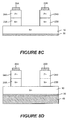
- FIG. 8A to 8D are schematic cross-sectional drawings illustrating methods of forming bidirectional transient voltage suppression devices according to some embodiments.
- FIG. 9 is a schematic cross-sectional drawing illustrating a bidirectional transient voltage suppression device according to further embodiments.
- FIG. 10 is a schematic cross-sectional drawing illustrating methods of forming bidirectional transient voltage suppression devices according to further embodiments.
- FIGS. 11A and 11B are schematic cross-sectional drawings illustrating bidirectional transient voltage suppression devices according to further embodiments.
- references herein to a layer formed “on” a substrate or other layer may refer to the layer formed directly on the substrate or other layer or on an intervening layer or layers formed on the substrate or other layer.
- references herein to a layer formed “on” a substrate or other layer may refer to the layer formed directly on the substrate or other layer or on an intervening layer or layers formed on the substrate or other layer.
- first and second elements or layers need not be in direct physical contact with one another, but may be connected by intervening conductive elements or layers which permit current flow between the first and second elements or layers.
- TVS transient voltage suppression
- Silicon carbide has been known for many years to have excellent physical and electronic properties which should theoretically allow production of electronic devices that can operate at higher temperatures, higher power and higher frequency than devices produced from silicon (Si) or GaAs.
- the high electric breakdown field of about 4 ⁇ 10 6 V/cm, high saturated electron drift velocity of about 2.0 ⁇ 10 7 cm/sec and high thermal conductivity of about 4.9 W/cm-K indicate that SiC would be suitable for high frequency, high power applications.
- SiC has not generally been considered ideal for use in a TVS device, because of the relatively high drift resistance of SiC, which can increase the Zener impedance of a Zener-diode based TVS device.
- Zener impedance is the differential resistance of a Zener diode based TVS device after the onset of current conduction. For better performance of the TVS device, it is desirable to reduce the Zener impedance of the device.
- silicon TVS devices are limited in the range of voltages they can handle due to the small bandgap of silicon. Thus, to provide for 15-20 Volts of protection, which may be required, for example, for protecting the gate of a silicon carbide based MOSFET, it may be necessary to connect several silicon based devices in series, which can increase circuit complexity and fabrication expense. Furthermore, silicon based TVS devices may be unable to withstand the high operating temperatures at which silicon carbide based devices can operate. For example, silicon based TVS devices typically have a maximum junction temperature of 185° C. In contrast, the operating temperature of a 4H—SiC MOSFET device can exceed 200° C.
- a circuit design must take into account the temperature limitations of a silicon-based TVS device so that the maximum operating temperature of the TVS device is not exceeded. However, it is generally preferable to place a TVS device as physically close to the device that it is protecting as possible.
- Some embodiments of the invention provide silicon carbide based transient voltage suppression devices using silicon carbide.
- some embodiments provide bidirectional silicon carbide based TVS devices having reduced Zener impedance.
- FIG. 1 a silicon carbide based bidirectional transient voltage suppressor (TVS) 100 is illustrated.
- FIG. 2 is a schematic equivalent circuit of the TVS 100 .
- the TVS 100 includes an n+ substrate 10 on which a pair of silicon carbide Zener diodes 20 A, 20 B are provided.
- the n+ substrate 10 can include 4H—SiC, although other polytypes of SiC, such as 6H, 3C or 15R can be used.
- the substrate 10 may include bulk silicon carbide. However, in other embodiments, the substrate 10 can include epitaxial silicon carbide.
- the Zener diodes 20 A, 20 B may be provided in the form of mesas, as illustrated in FIG. 1 .
- the Zener diodes 20 A, 20 B can be isolated by other methods, such as implant isolation.
- the Zener diodes 20 A, 20 B include respective n+ layers 22 A, 22 B in contact with the substrate 10 and p+ layers 24 A, 24 B forming respective Zener junctions 25 A, 25 B with the n+ layers 22 A, 22 B.
- the p+ layers 24 A, 24 B are separated from the substrate 10 by the respective n+ layers 22 A, 22 B.
- the n+ layers 22 A, 22 B may have a thickness of about 1 ⁇ m, while the p+ layers 24 A, 24 B may have a thickness of about 1.5 ⁇ m.
- the Zener junctions 25 A, 25 B may have respective areas of about 2500 ⁇ m 2 or more.
- the Zener junctions 25 A, 25 B may have dimensions of 500 ⁇ m ⁇ 500 ⁇ m, corresponding to areas of about 250,000 ⁇ m 2 .
- a Zener junction 25 A, 25 B may be capable of handling a current density greater than 1000 A/cm 2 .
- a TVS 100 may be capable of handling currents of up to 2.6 A or more, depending on the area of the Zener junctions 25 A, 25 B.
- a Zener junction 25 A, 25 B may have a Zener breakdown voltage V Z between 15V and 20V.
- Zener diode operation is based on Zener breakdown, which is a phenomenon that can occur across a junction between highly doped p- and n-type semiconductor layers.
- Zener breakdown when a heavily doped junction is reverse biased with a sufficient voltage, the energy barrier separating mobile carriers in one layer from empty states in the other layer becomes very narrow, permitting carriers to “tunnel” through the barrier and into the empty states, which results in current flow through the reverse biased junction. Such breakdown may occur in a controlled manner that does not damage the junction. It is therefore desirable for a transient voltage suppression device to utilize Zener breakdown for reverse bias conduction. Zener breakdown tends to occur at lower absolute voltages when the operating temperature of the device is elevated. Accordingly, a Zener diode may be characterized by having a negative temperature coefficient ( ⁇ ) in breakdown voltage.
- the n+ layers 22 A, 22 B may include 4H—SiC grown epitaxially on the substrate 10 and doped with n-type dopants, such as nitrogen, at a concentration of about 1 ⁇ 10 18 cm ⁇ 3 or more.
- the n+ layers 22 A, 22 B may have a doping concentration of 5 ⁇ 10 18 cm ⁇ 3 or greater, and in some embodiments may have a doping concentration of 2 ⁇ 10 19 cm ⁇ 3 .
- the p+ layers 24 A, 24 B may include 4H—SiC grown epitaxially on the respective n+ layers 22 A, 22 B and doped with p-type dopants, such as aluminum and/or boron, at a concentration of about 1 ⁇ 10 19 cm ⁇ 3 or more.
- the p+ layers 24 A, 24 B may have a doping concentration of 5 ⁇ 10 19 cm ⁇ 3 or greater, and in some embodiments may have a doping concentration of about 1 ⁇ 10 20 cm ⁇ 3 .
- the p+ layers 24 A, 24 B may have a higher doping concentration near an ohmic contact 26 A, 26 B formed thereon.
- the p+ layers 24 A, 24 B may have doping concentrations of 1 ⁇ 10 20 cm ⁇ 3 near the ohmic contacts 26 A, 26 B, and the doping concentrations may decrease to 5 ⁇ 10 19 cm ⁇ 3 for the remainder of the layers closer to the junctions 25 A, 25 B.
- the doping of the n+ layers 22 A, 22 B and the p+ layers 24 A, 24 B may determine the breakdown voltages of the respective Zener diodes 20 A, 20 B.
- Respective ohmic contacts 26 A, 26 B are formed on the p+ layers 24 A, 24 B opposite the n+ layers 22 A, 22 B. Furthermore, an ohmic contact 30 is formed on the substrate 10 opposite the Zener diodes 20 A, 20 B.
- a reference contact 42 can be made to the TVS 100 through the backside metallization 40 .
- the resistance of the substrate 10 which contributes to the Zener impedance of the TVS 100 , is represented in FIG. 2 by the resistances 27 A, 27 B.
- the substrate 10 can be thinned to a thickness of less than about 400 ⁇ m. In some embodiments, the substrate 10 can be thinned to a thickness of less than 200 ⁇ m. In some embodiments, the substrate 10 can be thinned to a thickness of less than 100 ⁇ m, and in some embodiments the substrate 10 can be thinned to a thickness of 10 ⁇ m.
- the substrate 10 can be thinned, for example, by mechanical polishing, grinding, etching, and/or a combination thereof. In some embodiments, the substrate 10 can be thinned prior to formation of the ohmic contact 30 thereon.
- the Zener diodes 20 A, 20 B may include mesas that extend through the n+ layers 22 A, 22 B and partially into the substrate 10 .
- the mesas may extend into, but not through an n+ layer 22 in which the n+ layers 22 A, 22 B are defined.
- FIGS. 4A and 4B Further embodiments are illustrated in FIGS. 4A and 4B . As shown therein, separate n+ layers s can be omitted, and the Zener junctions 25 A, 25 B can be formed directly between the p+ layers 24 A, 24 B and the substrate 10 . Furthermore, as shown in FIG. 4B , the Zener diodes 20 A, 20 B can be formed as mesas that extend completely through the p+ layers 24 A, 24 B and into the substrate 10 .
- a TVS 100 can be connected in parallel with a gate contact G of a silicon carbide MOSFET 110 .
- An input signal is applied to the SiC MOSFET 110 by an input drive unit 120 having an input resistance 122 . If the voltage applied by the input drive unit 120 experiences a voltage spike, TVS 100 starts to conduct, and the energy of the spike is dissipated through the TVS 100 , bypassing the sensitive gate of the MOSFET 110 .
- a single TVS 100 can clamp the input voltage level of the MOSFET 110 to +/ ⁇ 18V.
- the TVS 100 can operate at elevated temperatures, the TVS 100 can be mounted and/or formed very close to the MOSFET 110 .
- the TVS 100 can therefore provide a substantial improvement of reliability of power systems and power MOSFETs operating at high junction temperatures and/or high ambient temperatures.
- the TVS 100 and the MOSFET 110 can be integrated onto a common substrate.
- FIGS. 6 and 7 are graphs illustrating some current-voltage characteristics of bidirectional transient voltage suppression devices according to some embodiments.
- FIG. 6 illustrates the current-voltage characteristics 200 from a first contact 26 A to the reference contact 42 on a device having a Zener junction area of about 500 ⁇ m ⁇ 500 ⁇ m, or about 0.25 mm 2 .
- the characteristics illustrated in FIG. 6 show that the device had an operational voltage of approximately 16V and was capable of currents greater than 2.6 A, corresponding to a current density of 1040 A/cm 2 .
- FIG. 7 illustrates the temperature dependency of the current-voltage characteristics of a TVS 100 according to some embodiments.
- FIG. 7 illustrates the end-to-end current voltage characteristics of a bidirectional TVS 100 according to some embodiments at room temperature (curve 210 ) and at an elevated temperature of 250° C. (curve 212 ).
- the voltage protection of the TVS 100 dropped slightly from 18.8 volts to 18.3 volts when the temperature was raised to 250° C., meaning that the devices exhibited a negative temperature coefficient ( ⁇ ) in breakdown voltage.
- ⁇ negative temperature coefficient
- This behavior indicates that the voltage clamping in the SiC-based TVS 100 is based primarily on Zener breakdown, or band-to-band tunneling, as opposed to avalanche breakdown.
- the voltage change of 0.5V suggests that a TVS 100 according to embodiments of the present invention can also function as a high temperature voltage reference.
- FIGS. 8A to 8D illustrate the formation of a SiC TVS 100 according to some embodiments.
- an n+SiC substrate 10 A is provided.
- the substrate 10 A may include a bulk 4H—SiC substrate available from Cree, Inc., assignee of the present invention, that is doped with n-type dopants, such as silicon or arsenic, at a concentration of about 5 ⁇ 10 18 cm ⁇ 3 or more.
- the substrate 10 A may have a thickness of about 250 ⁇ m to about 500 ⁇ m.
- An n+ epitaxial layer 22 is formed on the n+ substrate 10 A, and a p+ epitaxial layer 24 is formed on the n+ epitaxial layer.
- the epitaxial layers may be formed, for example, using chemical vapor deposition. Epitaxial growth of silicon carbide is well known in the art.
- the n+ epitaxial layer 22 may have a thickness of about 1 ⁇ m and may be doped with n-type dopants, such as nitrogen, at a concentration of about 5 ⁇ 10 18 cm ⁇ 3 or more. In some embodiments, the n+ epitaxial layer 22 may have a doping concentration of 1 ⁇ 10 19 cm ⁇ 3 or greater, and in some embodiments may have a doping concentration of 2 ⁇ 10 19 cm ⁇ 3 .
- the p+ epitaxial layer 24 may have a thickness of about 1.5 ⁇ m and may be doped with p-type dopants, such as aluminum or boron, at a concentration of about 1 ⁇ 10 19 cm ⁇ 3 or more. In some embodiments, the p+ epitaxial layer 24 may have a doping concentration of 5 ⁇ 10 19 cm ⁇ 3 or greater, and in some embodiments may have a doping concentration of 1 ⁇ 10 20 cm ⁇ 3 . The doping of the p+ epitaxial layer 24 may be increased near a surface of the p+ epitaxial layer 24 opposite the n+ epitaxial layer 22 .
- p-type dopants such as aluminum or boron
- the p+ epitaxial layer 24 may have a doping concentration of 5 ⁇ 10 19 cm ⁇ 3 at the junction with the n+ epitaxial layer 22 , and the doping concentration may increase to 1 ⁇ 10 20 cm ⁇ 3 near the surface of the p+ epitaxial layer 24 opposite the n+ epitaxial layer 22 .
- an etch mask 35 which may comprise aluminum, may be formed on the p-type epitaxial layer 24 .
- the p-type epitaxial layer 24 and the n-type epitaxial layer 22 are then anisotropically etched to form mesas including n-type layers 22 A, 22 B and p-type layers 24 A, 24 B that respectively define Zener diodes 20 A, 20 B.
- Anisotropic etching of silicon carbide is well known in the art, and can be performed, for example, by dry etching the silicon carbide with a fluorine chemistry using an inductively coupled plasma (ICP) or reactive ion etch.
- the Zener diodes 20 A, 20 B can have junction areas of about 2500 ⁇ m 2 to about 250,000 ⁇ m 2 or more.
- ohmic contacts 26 A, 26 B are formed on the p-type layers 24 A, 24 B, respectively.
- the ohmic contacts 26 A, 26 B may comprise, for example, nickel, or nickel/aluminum, and may be annealed at a temperature of 775° C. for two minutes. Formation of low resistance ohmic contacts to heavily doped silicon carbide layers is well known in the art.
- a carrier substrate (not shown) may be affixed to the structure, and the substrate 10 A may be thinned to form a thinned substrate 10 .
- the carrier substrate may include a rigid material, such as silicon, alumina, sapphire, etc., and may be affixed using, for example, an adhesive film.
- the substrate 10 A may be thinned to form a substrate 10 having a thickness of less than about 400 ⁇ m. In some embodiments, the substrate 10 can have a thickness of less than 200 ⁇ m. In some embodiments, the substrate 10 can have a thickness of less than 100 ⁇ m, and in some embodiments the substrate 10 can have a thickness of 10 ⁇ m.
- Thinning of the substrate may be performed, for example, by etching and/or mechanically grinding, polishing or lapping the substrate until it has the desired thickness.
- a backside ohmic contact 30 may then be formed, for example, via laser annealing as described in U.S. Publication No. 2008/0311736, Dec. 18, 2008, the disclosure of which is incorporated herein by reference.
- a backside metallization 40 may be formed on the substrate 10 .
- the backside metallization may include, for example, a multilayer structure of Ti/TiW/Au including 1000 ⁇ of Ti, 1000 ⁇ of TiW, and 10,000 ⁇ of Au.
- the backside metallization 40 can be formed on the substrate 10 by sputtering, for example.
- the TVS device 100 may be conductively mounted, for example, to a metal submount or metal can, using the backside metallization 40 .
- FIG. 9 illustrates a bidirectional silicon carbide based transient voltage suppression (TVS) device 200 according to further embodiments.
- the silicon carbide based TVS device 200 illustrated in FIG. 9 includes an n+ silicon carbide base layer 210 , which may include a 4H—SiC bulk substrate.
- a pair of Zener diode mesas 220 A, 220 B are formed on opposite sides of the based layer 210 .
- the Zener diode mesas 220 A, 220 B include respective n+ layers 222 A, 222 B on the base layer 210 and p+ layers 224 A, 224 B on the respective n+ layers 222 A, 222 B, defining Zener junctions 225 A, 225 B therebetween.
- Ohmic contacts 226 A, 226 B are formed on the p+ layers 224 A, 224 B, respectively.
- the silicon carbide base layer 210 may be thinned to a thickness of less than 200 ⁇ m, thereby reducing the Zener impedance of the device.
- the doping ranges and thicknesses of the silicon carbide base layer 210 and the n+ layers 222 A, 222 B and p+ layers 224 A, 224 B, may be similar to those of the corresponding layers in the device illustrated in FIG. 1 .
- FIG. 10 is a schematic cross-sectional drawing illustrating methods of forming bidirectional transient voltage suppression devices according to further embodiments.
- a bidirectional transient voltage suppression device according to some embodiments can be formed using ion implantation.
- an n+ silicon carbide layer 210 is provided.
- the n+ silicon carbide layer 210 can include 4H—SiC, although other polytypes of SiC, such as 6H, 3C or 15R can be used.
- the n+ silicon carbide layer 210 may include bulk silicon carbide.
- the n+ silicon carbide layer 210 can include epitaxial silicon carbide.
- An implant mask 205 including a pair of openings 205 A, 205 B is formed on the silicon carbide layer 210 , and p-type dopants, such as aluminum, are selectively implanted into the silicon carbide layer 210 to form p+ regions 224 A, 224 B.
- the p+ regions 224 A, 224 B may be implanted with sufficient p-type dopants to cause the p+ regions 224 A, 224 B to form Zener junctions 225 A, 225 B with the n+ silicon carbide layer 210 , thereby defining respective Zener diodes 220 A, 220 B.
- the p+ regions 224 A, 224 B may be doped to have a net p-type dopant concentration of 1 ⁇ 10 19 cm ⁇ 3 or more.
- the p+ regions 224 A, 224 B may have a net p-type doping concentration of 5 ⁇ 10 19 cm ⁇ 3 or greater, and in some embodiments may have a net p-type doping concentration of about 1 ⁇ 10 20 cm ⁇ 3 .
- Suitable doping profiles can be obtained by implanting aluminum ions into a 4H—SiC layer according to one or more of the implant schedules shown in Tables 1 and 2 below.
- Table 1 describes an implant schedule for obtaining a box profile of aluminum ions in 4H—SiC having a doping concentration of about 1 ⁇ 10 19 cm ⁇ 3
- Table 2 describes an implant schedule for obtaining a box profile of aluminum ions in 4H—SiC having a doping concentration of about 5 ⁇ 10 18 cm ⁇ 3 .
- Implantation may be performed at an elevated temperature, such as about 650° C. to improve crystal quality.
- an activation anneal is performed in non-oxidizing ambient, such as argon, at a temperature of about 1500° C. to about 2200° C. for a duration of 1 min to 1 hours.
- the implants can be annealed at a temperature of 1650° C. for 5-30 min.
- Zener characteristics may be obtained once the p-type doping concentration exceeds about 5 ⁇ 10 19 cm ⁇ 3 (i.e., 5 ⁇ the implant schedule shown in Table 1).
- the resulting structure may be have a very thin intrinsic (i) layer between the p+ regions 224 A, 224 B and the silicon carbide layer 210 , and therefore may exhibit a mix of avalanche and Zener breakdown characteristics.
- the device may still function effectively as a transient voltage suppressor, however.
- FIGS. 11A and 11B are schematic cross-sectional drawing illustrating bidirectional transient voltage suppression devices 200 A, 200 B according to further embodiments.
- the TVS devices 200 A, 200 B are similar except that in the TVS device 200 A of FIG. 11A , the silicon carbide layer 210 is a bulk substrate of silicon carbide, while in the TVS device 200 B of FIG. 11B , the silicon carbide layer 210 is an epitaxial layer of silicon carbide on a bulk substrate 212 of silicon carbide.
- respective ohmic contacts 226 A, 226 B are formed on the p+ regions 224 A, 224 B.
- an ohmic contact 230 is formed on the silicon carbide layer 210 and/or the substrate 212 opposite the p+ regions 224 A, 224 B.
- the silicon carbide layer 210 and/or the substrate 212 can have a thickness of less than about 400 ⁇ m. In some embodiments, the substrate 212 can be thinned to a thickness of less than 200 ⁇ m. In some embodiments, the substrate 212 can be thinned to a thickness of less than 100 ⁇ m, and in some embodiments the substrate 212 can be thinned to a thickness of 10 ⁇ m.
- the substrate 212 can be thinned, for example, by mechanical polishing, grinding, etching, and/or a combination thereof. In some embodiments, the substrate 212 can be thinned prior to formation of the ohmic contact 230 thereon.
Landscapes
- Electrodes Of Semiconductors (AREA)
Abstract
Description
| TABLE 1 |
| 1 × 1019 cm−3 concentration, Implant 27A1+ |
| Dose (cm−2) | Energy (keV) | ||
| 3 × 10¹³ | 30 | ||
| 5 × 10¹³ | 65 | ||
| 8.5 × 10¹³ | 125 | ||
| 1.2 × 10¹⁴ | 220 | ||
| TABLE 2 |
| 5 × 1018 cm−3 concentration, Implant 27A1+ |
| Dose (cm−2) | Energy (keV) | ||
| 1.5 × 10¹³ | 30 | ||
| 2.5 × 10¹³ | 65 | ||
| 4.5 × 10¹³ | 125 | ||
| 7 × 10¹³ | 220 | ||
Claims (10)
Priority Applications (1)
| Application Number | Priority Date | Filing Date | Title |
|---|---|---|---|
| US13/860,955 US9312256B2 (en) | 2009-03-20 | 2013-04-11 | Bidirectional silicon carbide transient voltage supression devices |
Applications Claiming Priority (2)
| Application Number | Priority Date | Filing Date | Title |
|---|---|---|---|
| US12/408,167 US8445917B2 (en) | 2009-03-20 | 2009-03-20 | Bidirectional silicon carbide transient voltage suppression devices |
| US13/860,955 US9312256B2 (en) | 2009-03-20 | 2013-04-11 | Bidirectional silicon carbide transient voltage supression devices |
Related Parent Applications (1)
| Application Number | Title | Priority Date | Filing Date |
|---|---|---|---|
| US12/408,167 Division US8445917B2 (en) | 2009-03-20 | 2009-03-20 | Bidirectional silicon carbide transient voltage suppression devices |
Publications (2)
| Publication Number | Publication Date |
|---|---|
| US20130240908A1 US20130240908A1 (en) | 2013-09-19 |
| US9312256B2 true US9312256B2 (en) | 2016-04-12 |
Family
ID=42101616
Family Applications (2)
| Application Number | Title | Priority Date | Filing Date |
|---|---|---|---|
| US12/408,167 Active 2030-06-18 US8445917B2 (en) | 2009-03-20 | 2009-03-20 | Bidirectional silicon carbide transient voltage suppression devices |
| US13/860,955 Active US9312256B2 (en) | 2009-03-20 | 2013-04-11 | Bidirectional silicon carbide transient voltage supression devices |
Family Applications Before (1)
| Application Number | Title | Priority Date | Filing Date |
|---|---|---|---|
| US12/408,167 Active 2030-06-18 US8445917B2 (en) | 2009-03-20 | 2009-03-20 | Bidirectional silicon carbide transient voltage suppression devices |
Country Status (4)
| Country | Link |
|---|---|
| US (2) | US8445917B2 (en) |
| EP (1) | EP2409329B1 (en) |
| CN (1) | CN102428559B (en) |
| WO (1) | WO2010107510A1 (en) |
Families Citing this family (37)
| Publication number | Priority date | Publication date | Assignee | Title |
|---|---|---|---|---|
| WO2010110246A1 (en) * | 2009-03-25 | 2010-09-30 | ローム株式会社 | Semiconductor device |
| US10256094B2 (en) * | 2009-08-20 | 2019-04-09 | The Government Of The United States Of America, As Represented By The Secretary Of The Navy | Reduction of basal plane dislocations in epitaxial SiC using an in-situ etch process |
| FR2963983B1 (en) * | 2010-08-18 | 2012-09-07 | St Microelectronics Tours Sas | BIDIRECTIONAL DISSYMMETRIC PROTECTION COMPONENT |
| DE102011079569B4 (en) * | 2011-07-21 | 2013-11-07 | Hs Elektronik Systeme Gmbh | A power or power distribution system of an aircraft having an active transistor clamp and associated active level holding method |
| US8530902B2 (en) | 2011-10-26 | 2013-09-10 | General Electric Company | System for transient voltage suppressors |
| US8730629B2 (en) | 2011-12-22 | 2014-05-20 | General Electric Company | Variable breakdown transient voltage suppressor |
| US8835976B2 (en) * | 2012-03-14 | 2014-09-16 | General Electric Company | Method and system for ultra miniaturized packages for transient voltage suppressors |
| US9042072B2 (en) | 2012-03-30 | 2015-05-26 | General Electric Company | Method and system for lightning protection with distributed transient voltage suppression |
| EP2757688B1 (en) * | 2013-01-18 | 2019-05-22 | HS Elektronik Systeme GmbH | Active clamped transistor circuit for low temperature operating conditions |
| US8987858B2 (en) | 2013-03-18 | 2015-03-24 | General Electric Company | Method and system for transient voltage suppression |
| EP2976785A4 (en) * | 2013-03-21 | 2017-01-18 | Bourns, Inc. | Transient voltage suppressor, design and process |
| US9111750B2 (en) | 2013-06-28 | 2015-08-18 | General Electric Company | Over-voltage protection of gallium nitride semiconductor devices |
| US9997507B2 (en) | 2013-07-25 | 2018-06-12 | General Electric Company | Semiconductor assembly and method of manufacture |
| US9508841B2 (en) | 2013-08-01 | 2016-11-29 | General Electric Company | Method and system for a semiconductor device with integrated transient voltage suppression |
| KR101414005B1 (en) * | 2013-10-31 | 2014-07-04 | 주식회사 케이이씨 | Transient voltage suppressor and its manufacturing method |
| JP6539035B2 (en) * | 2014-01-08 | 2019-07-03 | ローム株式会社 | Chip parts |
| US9478606B2 (en) | 2014-02-13 | 2016-10-25 | Microsemi Corporation | SiC transient voltage suppressor |
| US10103540B2 (en) * | 2014-04-24 | 2018-10-16 | General Electric Company | Method and system for transient voltage suppression devices with active control |
| US9806157B2 (en) | 2014-10-03 | 2017-10-31 | General Electric Company | Structure and method for transient voltage suppression devices with a two-region base |
| CN105489657B (en) * | 2016-02-24 | 2016-11-23 | 江苏捷捷微电子股份有限公司 | A kind of one-way low pressure TVS device and manufacture method thereof |
| CN106024625B (en) * | 2016-07-23 | 2019-03-05 | 中国振华集团永光电子有限公司(国营第八七三厂) | A kind of highly reliable Flouride-resistani acid phesphatase glassivation voltage adjustment diode manufacturing method |
| CN106024624B (en) * | 2016-07-23 | 2019-03-05 | 中国振华集团永光电子有限公司(国营第八七三厂) | A kind of manufacturing method of highly reliable Flouride-resistani acid phesphatase transient voltage suppressor |
| CN107346967B (en) * | 2017-06-27 | 2021-01-15 | 联想(北京)有限公司 | Transient diode, signal transmission circuit and electronic equipment |
| CN107369681A (en) * | 2017-07-12 | 2017-11-21 | 战星罡 | Transient Voltage Suppressor and preparation method thereof |
| CN107833834A (en) * | 2017-09-29 | 2018-03-23 | 天水天光半导体有限责任公司 | A kind of manufacture method of transient voltage suppression diode chip |
| CN108701694B (en) * | 2018-03-27 | 2022-09-27 | 香港应用科技研究院有限公司 | High Voltage Silicon Carbide Schottky Diode Flip Chip Array |
| US10615292B2 (en) * | 2018-03-27 | 2020-04-07 | Hong Kong Applied Science And Technology Research Institute Co., Ltd. | High voltage silicon carbide Schottky diode flip chip array |
| US11374094B2 (en) * | 2018-08-29 | 2022-06-28 | Wuxi Nce Power Co., Ltd | Silicon carbide diode having high surge current capability and manufacturing method thereof |
| US10910501B2 (en) * | 2018-09-05 | 2021-02-02 | Monolith Semiconductor, Inc. | Stucture and method for SIC based protection device |
| TWI729538B (en) * | 2018-11-21 | 2021-06-01 | 大陸商上海瀚薪科技有限公司 | Silicon carbide semiconductor element integrated with clamping voltage clamping circuit |
| FR3093598B1 (en) * | 2019-03-05 | 2023-08-04 | St Microelectronics Srl | Surge protection device |
| DE102020126465A1 (en) * | 2020-10-08 | 2022-04-14 | Danfoss Silicon Power Gmbh | Power electronics module with an improved gate driver |
| CN112242449B (en) * | 2020-10-19 | 2023-04-18 | 重庆邮电大学 | Based on SiC substrate slot type MPS diode cell structure |
| US11830862B2 (en) * | 2020-11-12 | 2023-11-28 | Excellence Opto. Inc. | Chip structure of micro light-emitting diode display |
| CN116646352B (en) * | 2023-06-07 | 2024-12-31 | 上海晶岳电子有限公司 | LDMOS process TVS device and method for manufacturing the same |
| CN117174761B (en) * | 2023-11-02 | 2024-01-05 | 富芯微电子有限公司 | Voltage asymmetric bidirectional TVS device and manufacturing method thereof |
| CN117766378B (en) * | 2023-12-22 | 2024-08-09 | 上海领矽半导体有限公司 | Preparation method of silicon epitaxial material for low-capacitance TVS |
Citations (18)
| Publication number | Priority date | Publication date | Assignee | Title |
|---|---|---|---|---|
| US4174530A (en) | 1978-01-20 | 1979-11-13 | General Electric Company | Voltage surge arrester device |
| US4980315A (en) | 1988-07-18 | 1990-12-25 | General Instrument Corporation | Method of making a passivated P-N junction in mesa semiconductor structure |
| US5166769A (en) | 1988-07-18 | 1992-11-24 | General Instrument Corporation | Passitvated mesa semiconductor and method for making same |
| US5233214A (en) | 1989-09-14 | 1993-08-03 | Robert Bosch Gmbh | Controllable, temperature-compensated voltage limiter |
| US5528064A (en) | 1994-08-17 | 1996-06-18 | Texas Instruments Inc. | Structure for protecting integrated circuits from electro-static discharge |
| US5539604A (en) | 1994-09-30 | 1996-07-23 | Microsemi, Corp. | Transient voltage suppressor apparatus |
| US5760450A (en) | 1996-04-29 | 1998-06-02 | U.S. Philips Corporation | Semiconductor resistor using back-to-back zener diodes |
| US5880511A (en) | 1995-06-30 | 1999-03-09 | Semtech Corporation | Low-voltage punch-through transient suppressor employing a dual-base structure |
| EP1189286A1 (en) | 2000-03-06 | 2002-03-20 | Rohm Co., Ltd. | Semiconductor device |
| US6489660B1 (en) | 2001-05-22 | 2002-12-03 | General Semiconductor, Inc. | Low-voltage punch-through bi-directional transient-voltage suppression devices |
| US6515345B2 (en) | 2001-02-21 | 2003-02-04 | Semiconductor Components Industries Llc | Transient voltage suppressor with diode overlaying another diode for conserving space |
| US20030042538A1 (en) * | 2001-08-29 | 2003-03-06 | Rajesh Kumar | Silicon carbide power device having protective diode and method for manufacturing silicon carbide power device having protective diode |
| US7244970B2 (en) | 2004-12-22 | 2007-07-17 | Tyco Electronics Corporation | Low capacitance two-terminal barrier controlled TVS diodes |
| CN101009470A (en) | 2006-01-24 | 2007-08-01 | 孙玉华 | A power circuit for the calculating device |
| US7279724B2 (en) | 2004-02-25 | 2007-10-09 | Philips Lumileds Lighting Company, Llc | Ceramic substrate for a light emitting diode where the substrate incorporates ESD protection |
| US7339776B1 (en) | 2006-12-12 | 2008-03-04 | Pratt & Whitney Rocketdyne, Inc. | Silicon carbide diode voltage limiter |
| WO2008093789A1 (en) | 2007-01-31 | 2008-08-07 | The Kansai Electric Power Co., Inc. | Bipolar semiconductor device, method for manufacturing the bipolar semiconductor device and method for controlling zener voltage |
| US20090045457A1 (en) | 2006-11-16 | 2009-02-19 | Alpha & Omega Semiconductor, Ltd. | Optimized configurations to integrate steering diodes in low capacitance transient voltage suppressor (TVS) |
Family Cites Families (1)
| Publication number | Priority date | Publication date | Assignee | Title |
|---|---|---|---|---|
| US7851343B2 (en) | 2007-06-14 | 2010-12-14 | Cree, Inc. | Methods of forming ohmic layers through ablation capping layers |
-
2009
- 2009-03-20 US US12/408,167 patent/US8445917B2/en active Active
-
2010
- 2010-01-12 EP EP10703715.2A patent/EP2409329B1/en active Active
- 2010-01-12 WO PCT/US2010/020691 patent/WO2010107510A1/en not_active Ceased
- 2010-01-12 CN CN201080021983.7A patent/CN102428559B/en active Active
-
2013
- 2013-04-11 US US13/860,955 patent/US9312256B2/en active Active
Patent Citations (18)
| Publication number | Priority date | Publication date | Assignee | Title |
|---|---|---|---|---|
| US4174530A (en) | 1978-01-20 | 1979-11-13 | General Electric Company | Voltage surge arrester device |
| US4980315A (en) | 1988-07-18 | 1990-12-25 | General Instrument Corporation | Method of making a passivated P-N junction in mesa semiconductor structure |
| US5166769A (en) | 1988-07-18 | 1992-11-24 | General Instrument Corporation | Passitvated mesa semiconductor and method for making same |
| US5233214A (en) | 1989-09-14 | 1993-08-03 | Robert Bosch Gmbh | Controllable, temperature-compensated voltage limiter |
| US5528064A (en) | 1994-08-17 | 1996-06-18 | Texas Instruments Inc. | Structure for protecting integrated circuits from electro-static discharge |
| US5539604A (en) | 1994-09-30 | 1996-07-23 | Microsemi, Corp. | Transient voltage suppressor apparatus |
| US5880511A (en) | 1995-06-30 | 1999-03-09 | Semtech Corporation | Low-voltage punch-through transient suppressor employing a dual-base structure |
| US5760450A (en) | 1996-04-29 | 1998-06-02 | U.S. Philips Corporation | Semiconductor resistor using back-to-back zener diodes |
| EP1189286A1 (en) | 2000-03-06 | 2002-03-20 | Rohm Co., Ltd. | Semiconductor device |
| US6515345B2 (en) | 2001-02-21 | 2003-02-04 | Semiconductor Components Industries Llc | Transient voltage suppressor with diode overlaying another diode for conserving space |
| US6489660B1 (en) | 2001-05-22 | 2002-12-03 | General Semiconductor, Inc. | Low-voltage punch-through bi-directional transient-voltage suppression devices |
| US20030042538A1 (en) * | 2001-08-29 | 2003-03-06 | Rajesh Kumar | Silicon carbide power device having protective diode and method for manufacturing silicon carbide power device having protective diode |
| US7279724B2 (en) | 2004-02-25 | 2007-10-09 | Philips Lumileds Lighting Company, Llc | Ceramic substrate for a light emitting diode where the substrate incorporates ESD protection |
| US7244970B2 (en) | 2004-12-22 | 2007-07-17 | Tyco Electronics Corporation | Low capacitance two-terminal barrier controlled TVS diodes |
| CN101009470A (en) | 2006-01-24 | 2007-08-01 | 孙玉华 | A power circuit for the calculating device |
| US20090045457A1 (en) | 2006-11-16 | 2009-02-19 | Alpha & Omega Semiconductor, Ltd. | Optimized configurations to integrate steering diodes in low capacitance transient voltage suppressor (TVS) |
| US7339776B1 (en) | 2006-12-12 | 2008-03-04 | Pratt & Whitney Rocketdyne, Inc. | Silicon carbide diode voltage limiter |
| WO2008093789A1 (en) | 2007-01-31 | 2008-08-07 | The Kansai Electric Power Co., Inc. | Bipolar semiconductor device, method for manufacturing the bipolar semiconductor device and method for controlling zener voltage |
Non-Patent Citations (13)
| Title |
|---|
| "Transient Suppression Devices and Principles", Littelfuse, Inc., Application Note, Jan. 1998, 8 pages. |
| Chinese Office Action Corresponding to Chinese Patent Application No, 201080021983.7; Date of Issue: Jul. 26, 2013; Foreign Text, 10 Pages, English Translation Thereof, 9 Pages. |
| Chinese Office Action Corresponding to Chinese Patent Application No. 201080021983.7; Date of Issue: May 14, 2014; Foreign Text and English Translation, 18 Pages. |
| Hartwig, Bruce, "What is a Silicon Transient Voltage Suppressor and How Does It Work?" Vishay Semiconductors, Mar. 1, 2004, 2 pages. |
| International Preliminary Report on Patentability corresponding to International Application No. PCT/USI2010/020691; Date of Mailing: Mar. 31, 2011; 15 pages. |
| Ishii R. at al.: "20B-400A SiC Zener Diodes with Excellent Temperature Coefficient", Proceedings of the 19th International Symposium on Power Semiconductor Devices & ICs; May 27-30, 2007 Jeju, Korea, pp. 277-280, XP031129722. |
| Lepkowski, Jim, "An Introduction to Transient Voltage Suppression Devices," Semiconductor Components Industries, LLC, Jul. 2005, 8 pages. |
| Notification of Transmittal of the International Search Report and the Written Opinion of the International Searching Authority, or the Declaration; International Search Report; Written Opinion of the International Searching Authority corresponding to International application No. PCT/US/2010/020691; Date of mailing: Apr. 5, 2010; 15 pages. |
| Second Examination Report corresponding to European Patent Application No. 10703715.2; Date of mailing: Dec. 19; 2014; 5 pages. |
| Singh at al., "SiC Power Schottky Diodes in Power Factor Correction Circuits," Cree Application Note, 2002, 9 pages. |
| Vassilevski at al., "Low Voltage Silicon Carbide Zener Diode", Trans Tech Publications, Switzerland, 2004, 4 pages. |
| VASSiLEVSKI K V, et al.: "Low Voltage Silicon Carbide Zener Diode", Materials Science Forum vols. 457-460 (2004) pp, 1029-1032; Online at http://www.scientific.net, 2004 Trans Tech Publications, Switzerland. |
| Wikipedia, Transient voltage suppression diode, 2 pages, admitted prior art. |
Also Published As
| Publication number | Publication date |
|---|---|
| US8445917B2 (en) | 2013-05-21 |
| US20130240908A1 (en) | 2013-09-19 |
| EP2409329B1 (en) | 2019-08-21 |
| EP2409329A1 (en) | 2012-01-25 |
| US20100237356A1 (en) | 2010-09-23 |
| WO2010107510A1 (en) | 2010-09-23 |
| CN102428559B (en) | 2015-09-16 |
| CN102428559A (en) | 2012-04-25 |
Similar Documents
| Publication | Publication Date | Title |
|---|---|---|
| US9312256B2 (en) | Bidirectional silicon carbide transient voltage supression devices | |
| EP1845561B1 (en) | Semiconductor device including a heterojunction diode and manufacturing method thereof | |
| KR101260082B1 (en) | Normally-off integrated jfet power switches in wide bandgap semiconductors and methods of making | |
| US8952481B2 (en) | Super surge diodes | |
| KR101654975B1 (en) | Semiconductor assembly and method of manufacture | |
| US20080191304A1 (en) | Schottky Diode Structure with Silicon Mesa and Junction Barrier Schottky Wells | |
| US9093272B2 (en) | Methods of forming electronic elements with ESD protection | |
| CN102136501A (en) | Vertical-channel junction field-effect transistors having buried gates and methods of making the same | |
| WO2006124174A2 (en) | High voltage silicon carbide mos-bipolar devices having bi-directional blocking capabilities and methods of fabricating the same | |
| CN101647107A (en) | The avalanche protection that is used for wide bandgap devices | |
| CN104347616B (en) | Semiconductor subassembly and manufacture method | |
| WO2004079789A2 (en) | Interstage isolation in darlington transistors | |
| Huang et al. | Lateral implanted RESURF GaN MOSFETs with BV up to 2.5 kV | |
| EP1703561A2 (en) | Protection device for handling energy transients | |
| Huang et al. | Experimental demonstration of novel high-voltage epilayer RESURF GaN MOSFET | |
| EP4391041A1 (en) | High-electron-mobility transistor device with integrated p-n layer | |
| WO2019066974A1 (en) | Group iii-nitride antenna diode | |
| TW202013672A (en) | Protection device, SiC TVS device and manufacturing method thereof | |
| US12294018B2 (en) | Vertical power semiconductor device including silicon carbide (sic) semiconductor body | |
| Huang et al. | 730V, 34mΩ-cm 2 lateral epilayer RESURF GaN MOSFET | |
| Kizilyalli et al. | Very high performance GaN-on-GaN diodes | |
| Wang et al. | High-performance junction barrier Schottky rectifier with optimized structure | |
| Tournier et al. | Simulation study of a novel current limiting device: a vertical 6H-SiC etched AccuJFET | |
| EP0106072A2 (en) | High voltage Schottky barrier diode |
Legal Events
| Date | Code | Title | Description |
|---|---|---|---|
| STCF | Information on status: patent grant |
Free format text: PATENTED CASE |
|
| CC | Certificate of correction | ||
| MAFP | Maintenance fee payment |
Free format text: PAYMENT OF MAINTENANCE FEE, 4TH YEAR, LARGE ENTITY (ORIGINAL EVENT CODE: M1551); ENTITY STATUS OF PATENT OWNER: LARGE ENTITY Year of fee payment: 4 |
|
| AS | Assignment |
Owner name: U.S. BANK TRUST COMPANY, NATIONAL ASSOCIATION, NORTH CAROLINA Free format text: SECURITY INTEREST;ASSIGNOR:WOLFSPEED, INC.;REEL/FRAME:064185/0755 Effective date: 20230623 |
|
| MAFP | Maintenance fee payment |
Free format text: PAYMENT OF MAINTENANCE FEE, 8TH YEAR, LARGE ENTITY (ORIGINAL EVENT CODE: M1552); ENTITY STATUS OF PATENT OWNER: LARGE ENTITY Year of fee payment: 8 |
|
| AS | Assignment |
Owner name: U.S. BANK TRUST COMPANY, NATIONAL ASSOCIATION, AS COLLATERAL AGENT, TENNESSEE Free format text: NOTICE OF GRANT OF SECURITY INTEREST IN INTELLECTUAL PROPERTY;ASSIGNOR:WOLFSPEED, INC.;REEL/FRAME:072992/0113 Effective date: 20250929 Owner name: U.S. BANK TRUST COMPANY, NATIONAL ASSOCIATION, AS COLLATERAL AGENT, TENNESSEE Free format text: NOTICE OF GRANT OF SECURITY INTEREST IN INTELLECTUAL PROPERTY;ASSIGNOR:WOLFSPEED, INC.;REEL/FRAME:072992/0467 Effective date: 20250929 Owner name: WOLFSPEED, INC., NORTH CAROLINA Free format text: RELEASE OF SECURITY INTEREST IN INTELLECTUAL PROPERTY COLLATERAL AT REEL/FRAME NO. 64185/0755;ASSIGNOR:U.S. BANK TRUST COMPANY, NATIONAL ASSOCIATION, AS COLLATERAL AGENT;REEL/FRAME:072989/0001 Effective date: 20250929 Owner name: U.S. BANK TRUST COMPANY, NATIONAL ASSOCIATION, AS COLLATERAL AGENT, TENNESSEE Free format text: NOTICE OF GRANT OF SECURITY INTEREST IN INTELLECTUAL PROPERTY;ASSIGNOR:WOLFSPEED, INC.;REEL/FRAME:072992/0381 Effective date: 20250929 Owner name: U.S. BANK TRUST COMPANY, NATIONAL ASSOCIATION, AS COLLATERAL AGENT, TENNESSEE Free format text: NOTICE OF GRANT OF SECURITY INTEREST IN INTELLECTUAL PROPERTY;ASSIGNOR:WOLFSPEED, INC.;REEL/FRAME:072992/0588 Effective date: 20250929 |