US9312231B2 - Method and apparatus for high temperature semiconductor device packages and structures using a low temperature process - Google Patents
Method and apparatus for high temperature semiconductor device packages and structures using a low temperature process Download PDFInfo
- Publication number
- US9312231B2 US9312231B2 US14/068,496 US201314068496A US9312231B2 US 9312231 B2 US9312231 B2 US 9312231B2 US 201314068496 A US201314068496 A US 201314068496A US 9312231 B2 US9312231 B2 US 9312231B2
- Authority
- US
- United States
- Prior art keywords
- silver
- semiconductor device
- sintered silver
- package
- device package
- Prior art date
- Legal status (The legal status is an assumption and is not a legal conclusion. Google has not performed a legal analysis and makes no representation as to the accuracy of the status listed.)
- Active
Links
Images


Classifications
-
- H01L24/13—
-
- H—ELECTRICITY
- H10—SEMICONDUCTOR DEVICES; ELECTRIC SOLID-STATE DEVICES NOT OTHERWISE PROVIDED FOR
- H10W—GENERIC PACKAGES, INTERCONNECTIONS, CONNECTORS OR OTHER CONSTRUCTIONAL DETAILS OF DEVICES COVERED BY CLASS H10
- H10W72/00—Interconnections or connectors in packages
- H10W72/30—Die-attach connectors
-
- H01L21/50—
-
- H01L23/057—
-
- H01L23/142—
-
- H01L23/3677—
-
- H01L24/80—
-
- H—ELECTRICITY
- H10—SEMICONDUCTOR DEVICES; ELECTRIC SOLID-STATE DEVICES NOT OTHERWISE PROVIDED FOR
- H10P—GENERIC PROCESSES OR APPARATUS FOR THE MANUFACTURE OR TREATMENT OF DEVICES COVERED BY CLASS H10
- H10P14/00—Formation of materials, e.g. in the shape of layers or pillars
- H10P14/40—Formation of materials, e.g. in the shape of layers or pillars of conductive or resistive materials
- H10P14/46—Formation of materials, e.g. in the shape of layers or pillars of conductive or resistive materials using a liquid
-
- H—ELECTRICITY
- H10—SEMICONDUCTOR DEVICES; ELECTRIC SOLID-STATE DEVICES NOT OTHERWISE PROVIDED FOR
- H10W—GENERIC PACKAGES, INTERCONNECTIONS, CONNECTORS OR OTHER CONSTRUCTIONAL DETAILS OF DEVICES COVERED BY CLASS H10
- H10W40/00—Arrangements for thermal protection or thermal control
- H10W40/20—Arrangements for cooling
- H10W40/22—Arrangements for cooling characterised by their shape, e.g. having conical or cylindrical projections
- H10W40/226—Arrangements for cooling characterised by their shape, e.g. having conical or cylindrical projections characterised by projecting parts, e.g. fins to increase surface area
- H10W40/228—Arrangements for cooling characterised by their shape, e.g. having conical or cylindrical projections characterised by projecting parts, e.g. fins to increase surface area the projecting parts being wire-shaped or pin-shaped
-
- H—ELECTRICITY
- H10—SEMICONDUCTOR DEVICES; ELECTRIC SOLID-STATE DEVICES NOT OTHERWISE PROVIDED FOR
- H10W—GENERIC PACKAGES, INTERCONNECTIONS, CONNECTORS OR OTHER CONSTRUCTIONAL DETAILS OF DEVICES COVERED BY CLASS H10
- H10W70/00—Package substrates; Interposers; Redistribution layers [RDL]
- H10W70/01—Manufacture or treatment
- H10W70/05—Manufacture or treatment of insulating or insulated package substrates, or of interposers, or of redistribution layers
- H10W70/095—Manufacture or treatment of insulating or insulated package substrates, or of interposers, or of redistribution layers of vias therein
-
- H—ELECTRICITY
- H10—SEMICONDUCTOR DEVICES; ELECTRIC SOLID-STATE DEVICES NOT OTHERWISE PROVIDED FOR
- H10W—GENERIC PACKAGES, INTERCONNECTIONS, CONNECTORS OR OTHER CONSTRUCTIONAL DETAILS OF DEVICES COVERED BY CLASS H10
- H10W70/00—Package substrates; Interposers; Redistribution layers [RDL]
- H10W70/01—Manufacture or treatment
- H10W70/05—Manufacture or treatment of insulating or insulated package substrates, or of interposers, or of redistribution layers
- H10W70/098—Applying pastes or inks, e.g. screen printing
-
- H—ELECTRICITY
- H10—SEMICONDUCTOR DEVICES; ELECTRIC SOLID-STATE DEVICES NOT OTHERWISE PROVIDED FOR
- H10W—GENERIC PACKAGES, INTERCONNECTIONS, CONNECTORS OR OTHER CONSTRUCTIONAL DETAILS OF DEVICES COVERED BY CLASS H10
- H10W70/00—Package substrates; Interposers; Redistribution layers [RDL]
- H10W70/20—Conductive package substrates serving as an interconnection, e.g. metal plates
- H10W70/24—Conductive package substrates serving as an interconnection, e.g. metal plates characterised by materials
-
- H—ELECTRICITY
- H10—SEMICONDUCTOR DEVICES; ELECTRIC SOLID-STATE DEVICES NOT OTHERWISE PROVIDED FOR
- H10W—GENERIC PACKAGES, INTERCONNECTIONS, CONNECTORS OR OTHER CONSTRUCTIONAL DETAILS OF DEVICES COVERED BY CLASS H10
- H10W70/00—Package substrates; Interposers; Redistribution layers [RDL]
- H10W70/40—Leadframes
- H10W70/479—Leadframes on or in insulating or insulated package substrates, interposers, or redistribution layers
-
- H—ELECTRICITY
- H10—SEMICONDUCTOR DEVICES; ELECTRIC SOLID-STATE DEVICES NOT OTHERWISE PROVIDED FOR
- H10W—GENERIC PACKAGES, INTERCONNECTIONS, CONNECTORS OR OTHER CONSTRUCTIONAL DETAILS OF DEVICES COVERED BY CLASS H10
- H10W70/00—Package substrates; Interposers; Redistribution layers [RDL]
- H10W70/60—Insulating or insulated package substrates; Interposers; Redistribution layers
- H10W70/62—Insulating or insulated package substrates; Interposers; Redistribution layers characterised by their interconnections
- H10W70/66—Conductive materials thereof
-
- H—ELECTRICITY
- H10—SEMICONDUCTOR DEVICES; ELECTRIC SOLID-STATE DEVICES NOT OTHERWISE PROVIDED FOR
- H10W—GENERIC PACKAGES, INTERCONNECTIONS, CONNECTORS OR OTHER CONSTRUCTIONAL DETAILS OF DEVICES COVERED BY CLASS H10
- H10W70/00—Package substrates; Interposers; Redistribution layers [RDL]
- H10W70/60—Insulating or insulated package substrates; Interposers; Redistribution layers
- H10W70/67—Insulating or insulated package substrates; Interposers; Redistribution layers characterised by their insulating layers or insulating parts
- H10W70/68—Shapes or dispositions thereof
- H10W70/6875—Shapes or dispositions thereof being on a metallic substrate, e.g. insulated metal substrates [IMS]
-
- H—ELECTRICITY
- H10—SEMICONDUCTOR DEVICES; ELECTRIC SOLID-STATE DEVICES NOT OTHERWISE PROVIDED FOR
- H10W—GENERIC PACKAGES, INTERCONNECTIONS, CONNECTORS OR OTHER CONSTRUCTIONAL DETAILS OF DEVICES COVERED BY CLASS H10
- H10W72/00—Interconnections or connectors in packages
- H10W72/20—Bump connectors, e.g. solder bumps or copper pillars; Dummy bumps; Thermal bumps
-
- H—ELECTRICITY
- H10—SEMICONDUCTOR DEVICES; ELECTRIC SOLID-STATE DEVICES NOT OTHERWISE PROVIDED FOR
- H10W—GENERIC PACKAGES, INTERCONNECTIONS, CONNECTORS OR OTHER CONSTRUCTIONAL DETAILS OF DEVICES COVERED BY CLASS H10
- H10W72/00—Interconnections or connectors in packages
- H10W72/50—Bond wires
-
- H—ELECTRICITY
- H10—SEMICONDUCTOR DEVICES; ELECTRIC SOLID-STATE DEVICES NOT OTHERWISE PROVIDED FOR
- H10W—GENERIC PACKAGES, INTERCONNECTIONS, CONNECTORS OR OTHER CONSTRUCTIONAL DETAILS OF DEVICES COVERED BY CLASS H10
- H10W74/00—Encapsulations, e.g. protective coatings
- H10W74/10—Encapsulations, e.g. protective coatings characterised by their shape or disposition
- H10W74/111—Encapsulations, e.g. protective coatings characterised by their shape or disposition the semiconductor body being completely enclosed
- H10W74/114—Encapsulations, e.g. protective coatings characterised by their shape or disposition the semiconductor body being completely enclosed by a substrate and the encapsulations
-
- H—ELECTRICITY
- H10—SEMICONDUCTOR DEVICES; ELECTRIC SOLID-STATE DEVICES NOT OTHERWISE PROVIDED FOR
- H10W—GENERIC PACKAGES, INTERCONNECTIONS, CONNECTORS OR OTHER CONSTRUCTIONAL DETAILS OF DEVICES COVERED BY CLASS H10
- H10W76/00—Containers; Fillings or auxiliary members therefor; Seals
- H10W76/10—Containers or parts thereof
- H10W76/12—Containers or parts thereof characterised by their shape
- H10W76/13—Containers comprising a conductive base serving as an interconnection
- H10W76/134—Containers comprising a conductive base serving as an interconnection having other interconnections parallel to the conductive base
-
- H—ELECTRICITY
- H10—SEMICONDUCTOR DEVICES; ELECTRIC SOLID-STATE DEVICES NOT OTHERWISE PROVIDED FOR
- H10W—GENERIC PACKAGES, INTERCONNECTIONS, CONNECTORS OR OTHER CONSTRUCTIONAL DETAILS OF DEVICES COVERED BY CLASS H10
- H10W76/00—Containers; Fillings or auxiliary members therefor; Seals
- H10W76/10—Containers or parts thereof
- H10W76/12—Containers or parts thereof characterised by their shape
- H10W76/15—Containers comprising an insulating or insulated base
- H10W76/157—Containers comprising an insulating or insulated base having interconnections parallel to the insulating or insulated base
-
- H—ELECTRICITY
- H10—SEMICONDUCTOR DEVICES; ELECTRIC SOLID-STATE DEVICES NOT OTHERWISE PROVIDED FOR
- H10W—GENERIC PACKAGES, INTERCONNECTIONS, CONNECTORS OR OTHER CONSTRUCTIONAL DETAILS OF DEVICES COVERED BY CLASS H10
- H10W90/00—Package configurations
-
- H—ELECTRICITY
- H10—SEMICONDUCTOR DEVICES; ELECTRIC SOLID-STATE DEVICES NOT OTHERWISE PROVIDED FOR
- H10W—GENERIC PACKAGES, INTERCONNECTIONS, CONNECTORS OR OTHER CONSTRUCTIONAL DETAILS OF DEVICES COVERED BY CLASS H10
- H10W95/00—Packaging processes not covered by the other groups of this subclass
-
- H—ELECTRICITY
- H10—SEMICONDUCTOR DEVICES; ELECTRIC SOLID-STATE DEVICES NOT OTHERWISE PROVIDED FOR
- H10W—GENERIC PACKAGES, INTERCONNECTIONS, CONNECTORS OR OTHER CONSTRUCTIONAL DETAILS OF DEVICES COVERED BY CLASS H10
- H10W99/00—Subject matter not provided for in other groups of this subclass
-
- H01L2224/05599—
-
- H01L2224/29339—
-
- H01L2224/45099—
-
- H01L2224/48091—
-
- H01L2224/48137—
-
- H01L2224/48247—
-
- H01L2224/83447—
-
- H01L2224/8384—
-
- H01L23/3121—
-
- H01L24/32—
-
- H01L24/48—
-
- H01L2924/00—
-
- H01L2924/00014—
-
- H01L2924/16152—
-
- H01L2924/16598—
-
- H01L2924/171—
-
- H01L2924/181—
-
- H—ELECTRICITY
- H10—SEMICONDUCTOR DEVICES; ELECTRIC SOLID-STATE DEVICES NOT OTHERWISE PROVIDED FOR
- H10W—GENERIC PACKAGES, INTERCONNECTIONS, CONNECTORS OR OTHER CONSTRUCTIONAL DETAILS OF DEVICES COVERED BY CLASS H10
- H10W72/00—Interconnections or connectors in packages
- H10W72/01—Manufacture or treatment
- H10W72/013—Manufacture or treatment of die-attach connectors
- H10W72/01321—Manufacture or treatment of die-attach connectors using local deposition
- H10W72/01323—Manufacture or treatment of die-attach connectors using local deposition in liquid form, e.g. by dispensing droplets or by screen printing
-
- H—ELECTRICITY
- H10—SEMICONDUCTOR DEVICES; ELECTRIC SOLID-STATE DEVICES NOT OTHERWISE PROVIDED FOR
- H10W—GENERIC PACKAGES, INTERCONNECTIONS, CONNECTORS OR OTHER CONSTRUCTIONAL DETAILS OF DEVICES COVERED BY CLASS H10
- H10W72/00—Interconnections or connectors in packages
- H10W72/071—Connecting or disconnecting
- H10W72/073—Connecting or disconnecting of die-attach connectors
- H10W72/07331—Connecting techniques
-
- H—ELECTRICITY
- H10—SEMICONDUCTOR DEVICES; ELECTRIC SOLID-STATE DEVICES NOT OTHERWISE PROVIDED FOR
- H10W—GENERIC PACKAGES, INTERCONNECTIONS, CONNECTORS OR OTHER CONSTRUCTIONAL DETAILS OF DEVICES COVERED BY CLASS H10
- H10W72/00—Interconnections or connectors in packages
- H10W72/30—Die-attach connectors
- H10W72/321—Structures or relative sizes of die-attach connectors
- H10W72/325—Die-attach connectors having a filler embedded in a matrix
-
- H—ELECTRICITY
- H10—SEMICONDUCTOR DEVICES; ELECTRIC SOLID-STATE DEVICES NOT OTHERWISE PROVIDED FOR
- H10W—GENERIC PACKAGES, INTERCONNECTIONS, CONNECTORS OR OTHER CONSTRUCTIONAL DETAILS OF DEVICES COVERED BY CLASS H10
- H10W72/00—Interconnections or connectors in packages
- H10W72/30—Die-attach connectors
- H10W72/351—Materials of die-attach connectors
- H10W72/352—Materials of die-attach connectors comprising metals or metalloids, e.g. solders
-
- H—ELECTRICITY
- H10—SEMICONDUCTOR DEVICES; ELECTRIC SOLID-STATE DEVICES NOT OTHERWISE PROVIDED FOR
- H10W—GENERIC PACKAGES, INTERCONNECTIONS, CONNECTORS OR OTHER CONSTRUCTIONAL DETAILS OF DEVICES COVERED BY CLASS H10
- H10W72/00—Interconnections or connectors in packages
- H10W72/50—Bond wires
- H10W72/541—Dispositions of bond wires
- H10W72/5445—Dispositions of bond wires being orthogonal to a side surface of the chip, e.g. parallel arrangements
-
- H—ELECTRICITY
- H10—SEMICONDUCTOR DEVICES; ELECTRIC SOLID-STATE DEVICES NOT OTHERWISE PROVIDED FOR
- H10W—GENERIC PACKAGES, INTERCONNECTIONS, CONNECTORS OR OTHER CONSTRUCTIONAL DETAILS OF DEVICES COVERED BY CLASS H10
- H10W72/00—Interconnections or connectors in packages
- H10W72/851—Dispositions of multiple connectors or interconnections
- H10W72/874—On different surfaces
- H10W72/884—Die-attach connectors and bond wires
-
- H—ELECTRICITY
- H10—SEMICONDUCTOR DEVICES; ELECTRIC SOLID-STATE DEVICES NOT OTHERWISE PROVIDED FOR
- H10W—GENERIC PACKAGES, INTERCONNECTIONS, CONNECTORS OR OTHER CONSTRUCTIONAL DETAILS OF DEVICES COVERED BY CLASS H10
- H10W72/00—Interconnections or connectors in packages
- H10W72/90—Bond pads, in general
- H10W72/951—Materials of bond pads
- H10W72/952—Materials of bond pads comprising metals or metalloids, e.g. PbSn, Ag or Cu
-
- H—ELECTRICITY
- H10—SEMICONDUCTOR DEVICES; ELECTRIC SOLID-STATE DEVICES NOT OTHERWISE PROVIDED FOR
- H10W—GENERIC PACKAGES, INTERCONNECTIONS, CONNECTORS OR OTHER CONSTRUCTIONAL DETAILS OF DEVICES COVERED BY CLASS H10
- H10W74/00—Encapsulations, e.g. protective coatings
-
- H—ELECTRICITY
- H10—SEMICONDUCTOR DEVICES; ELECTRIC SOLID-STATE DEVICES NOT OTHERWISE PROVIDED FOR
- H10W—GENERIC PACKAGES, INTERCONNECTIONS, CONNECTORS OR OTHER CONSTRUCTIONAL DETAILS OF DEVICES COVERED BY CLASS H10
- H10W76/00—Containers; Fillings or auxiliary members therefor; Seals
- H10W76/10—Containers or parts thereof
-
- H—ELECTRICITY
- H10—SEMICONDUCTOR DEVICES; ELECTRIC SOLID-STATE DEVICES NOT OTHERWISE PROVIDED FOR
- H10W—GENERIC PACKAGES, INTERCONNECTIONS, CONNECTORS OR OTHER CONSTRUCTIONAL DETAILS OF DEVICES COVERED BY CLASS H10
- H10W76/00—Containers; Fillings or auxiliary members therefor; Seals
- H10W76/60—Seals
- H10W76/67—Seals characterised by their materials
-
- H—ELECTRICITY
- H10—SEMICONDUCTOR DEVICES; ELECTRIC SOLID-STATE DEVICES NOT OTHERWISE PROVIDED FOR
- H10W—GENERIC PACKAGES, INTERCONNECTIONS, CONNECTORS OR OTHER CONSTRUCTIONAL DETAILS OF DEVICES COVERED BY CLASS H10
- H10W90/00—Package configurations
- H10W90/701—Package configurations characterised by the relative positions of pads or connectors relative to package parts
- H10W90/731—Package configurations characterised by the relative positions of pads or connectors relative to package parts of die-attach connectors
- H10W90/736—Package configurations characterised by the relative positions of pads or connectors relative to package parts of die-attach connectors between a chip and a stacked lead frame, conducting package substrate or heat sink
-
- H—ELECTRICITY
- H10—SEMICONDUCTOR DEVICES; ELECTRIC SOLID-STATE DEVICES NOT OTHERWISE PROVIDED FOR
- H10W—GENERIC PACKAGES, INTERCONNECTIONS, CONNECTORS OR OTHER CONSTRUCTIONAL DETAILS OF DEVICES COVERED BY CLASS H10
- H10W90/00—Package configurations
- H10W90/701—Package configurations characterised by the relative positions of pads or connectors relative to package parts
- H10W90/751—Package configurations characterised by the relative positions of pads or connectors relative to package parts of bond wires
- H10W90/753—Package configurations characterised by the relative positions of pads or connectors relative to package parts of bond wires between laterally-adjacent chips
-
- H—ELECTRICITY
- H10—SEMICONDUCTOR DEVICES; ELECTRIC SOLID-STATE DEVICES NOT OTHERWISE PROVIDED FOR
- H10W—GENERIC PACKAGES, INTERCONNECTIONS, CONNECTORS OR OTHER CONSTRUCTIONAL DETAILS OF DEVICES COVERED BY CLASS H10
- H10W90/00—Package configurations
- H10W90/701—Package configurations characterised by the relative positions of pads or connectors relative to package parts
- H10W90/751—Package configurations characterised by the relative positions of pads or connectors relative to package parts of bond wires
- H10W90/754—Package configurations characterised by the relative positions of pads or connectors relative to package parts of bond wires between a chip and a stacked insulating package substrate, interposer or RDL
-
- H—ELECTRICITY
- H10—SEMICONDUCTOR DEVICES; ELECTRIC SOLID-STATE DEVICES NOT OTHERWISE PROVIDED FOR
- H10W—GENERIC PACKAGES, INTERCONNECTIONS, CONNECTORS OR OTHER CONSTRUCTIONAL DETAILS OF DEVICES COVERED BY CLASS H10
- H10W90/00—Package configurations
- H10W90/701—Package configurations characterised by the relative positions of pads or connectors relative to package parts
- H10W90/751—Package configurations characterised by the relative positions of pads or connectors relative to package parts of bond wires
- H10W90/756—Package configurations characterised by the relative positions of pads or connectors relative to package parts of bond wires between a chip and a stacked lead frame, conducting package substrate or heat sink
Definitions
- This disclosure relates generally to semiconductor device packaging, and more specifically, to a low-temperature process for fabricating high temperature and high performance semiconductor device packages.
- a variety of semiconductor device packages include a combination of ceramic, organic, and metallic materials. In order to form a usable structure for the semiconductor device package, these differing materials are in contact with one another. These differing materials often have significantly different material properties that can cause failures of a semiconductor device package incorporating the materials. It is therefore desirable to have semiconductor device packages that incorporate materials having differing material properties but that are not subject to failures due to the differing material properties (e.g., coefficient of thermal expansion).
- FIG. 1 is a simplified block diagram illustrating a cross-sectional view of an air cavity package.
- FIG. 2 is a simplified block diagram illustrating a plan view of the air cavity package.
- FIG. 3 is a simplified block diagram of a cross sectional view of a system at a stage in processing in which device die are coupled to metal coins or slugs embedded in a PCB or other package substrate.
- FIG. 4 is a simplified block diagram of a cross sectional view of a system at a stage in processing in which device die are coupled to sintered silver vias in a PCB or other package substrate.
- FIG. 5 is a simplified block diagram of a cross sectional view of a system at a stage in processing in which a copper slug is incorporated in a sintered silver large via.
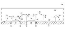
- FIG. 6 is a simplified block diagram of a cross sectional view of a system at a stage in processing in which a pair of metal slugs are incorporated in a sintered silver large via.
- FIG. 7 is a simplified block diagram of a cross sectional view of a system at a stage in processing in which a passive component is incorporated in a sintered silver large via.
- Embodiments of the present invention provide for a semiconductor device package that incorporates a combination of ceramic, organic, and metallic materials that are coupled using silver.
- the silver is applied in the form of fine particles (e.g., nano particle silver) under pressure and a low temperature (e.g., sintering at 250° C.).
- the silver forms a solid that has a typical melting point of silver (i.e., approximately 962° C.), and therefore the finished package can withstand temperatures significantly higher than the manufacturing temperature.
- the silver is an interfacial material between the various combined materials, the effect of differing material properties between ceramic, organic, and metallic components, such as coefficient of thermal expansion, is reduced due to low temperature of bonding and the ductility of the silver.
- the silver can be used in place of or in conjunction with copper slugs in printed circuit boards for attachment of heat sinks or large through vias. Such embodiments provide a thinner PCB than is typical for included copper slugs.
- Different types of high performance semiconductor device packages incorporate a combination of ceramic, organic, and metallic materials. But differing property characteristics of these materials can cause failures in the resultant package. For example, widely differing coefficients of thermal expansion between ceramic and copper can cause high stress in the package that can cause warping and cracking of the package near the connection between these materials.
- Air cavity packages typically includes one or more semiconductor device die attached to a base plate and an insulative window frame surrounding the die. A cap is placed over the window frame, sealing the die in a cavity of air.
- Air cavity packages can be used to house high frequency devices such as radio-frequency (RF) die. Packaging a high frequency semiconductor device in encapsulated air can improve high frequency properties of the die and electrical leads, as compared to encapsulation in a molding compound that has a higher dielectric constant than air.
- RF radio-frequency
- FIG. 1 is a simplified block diagram illustrating a cross-sectional view of an air cavity package 100 .
- FIG. 2 is a simplified block diagram illustrating a plan view of air cavity package 100 .
- An air cavity package uses a conductive metal base plate 110 that can incorporate a die attach region 120 .
- a window frame 130 made of a ceramic material is attached to the conductive metal base plate.
- Window frame 130 is generally attached to the conductive metal base plate prior to a die attach process.
- Conductive leads 140 are disposed on a top surface of the window frame and are used to make electrical contact 142 and 144 to a die 150 included in the package.
- Conductive leads 140 can be inserted into a recess along the top of window frame 130 .
- a cap 160 is attached to the top of the leads and the window frame, which seals a cavity 170 .
- conductive metal base plate 110 is typically made of a CuMOCu or Cu(CuMo)Cu laminate or CuW when a ceramic window frame is used. But both CuMOCu and Cu(CuMo)Cu laminates, as well as CuW, have significantly lower thermal conductivity than pure copper, which reduces the overall thermal performance of the package.
- epoxies can be used to attach a ceramic window frame to a metal base plate prior to die attach, epoxies can be damaged during subsequent high temperature die attach processes and thereby have a lower reliability. While some conventional air cavity techniques can involve attaching the window frame after die attach, those window frames are typically constructed of plastic which has a much lower thermal conductivity and capacitance than a ceramic window frame. This can limit the use of air cavity packages with plastic window frames to lower power applications.
- Embodiments of the present invention provide for using silver as an interface material between ceramic window frame 130 and both conductive metal base plate 110 and conductive leads 140 (e.g., at interface regions 175 and 180 ).
- the silver is applied using a low-temperature sintering technique in which a fine particle silver paste, powder, or film is applied to the region of interest under heat and pressure.
- the silver particles are of nanoscale, and therefore surface energies of the molecules forming the particles can dominate interactions between the particles, including surface tension, thereby allowing for formation of solid silver at a temperature significantly lower than the melting point of silver.
- a typical melting point of the silver applies (i.e., approximately 960° C.).
- a silver sintering process can be performed by applying fine particle silver to conductive metal base plate 110 at interface region 175 .
- Ceramic window frame 130 is then applied to the fine particle silver at a temperature and pressure sufficient to cause the silver particles to bond to one another and to the materials of the ceramic window frame and the conductive metal base plate.
- the ceramic window frame can be metalized using a number of metalizing techniques known in the art (metallization layer 135 ).
- the ceramic window frame can be metalized using a direct plated copper process, a directed bonded copper process, a refractory metal fire plus nickel/gold plating, or a thin film process using TiNiAu, TiW, gold, and the like.
- the temperature used during the sintering process is between approximately 200-300° C., and typically around 250° C., well below brazing temperatures used for prior art air cavity packages.
- fine particle silver can be applied at interface region 180 on ceramic window frame 130 and conductive leads 140 can be applied under a temperature and pressure to cause the silver particles to bond.
- the sintered silver at the interfaces provides a dual effect, an adhesive coupling of the differing materials together and an electrical/thermal coupling.
- Fine particle silver can be applied using a variety of techniques.
- a paste containing the fine particle silver can be used. Such a paste can be sprayed on, printed on, or otherwise applied.
- a powder form of the fine particle silver can also be used, and applied using similar methods.
- a pre-formed film incorporating fine particle silver and organic materials can be used by placing the film between parts desired to be bonded under a low temperature (e.g., 250° C.) and added pressure. The organic material of the film is removed under such process conditions and the solid silver is formed.
- conductive metal base plate 110 Since the bonding process is performed at significantly lower temperatures than that of prior art brazing techniques, effects due to the differing CTE of ceramic and metal are avoided (e.g., ceramic cracking and warping). Further, less expensive and more efficient materials can be used for conductive metal base plate 110 . For example, a solid copper flange can be used instead of a laminate flange as the conductive metal base plate. In addition, conductive leads 140 can be formed of a solid copper rather than an alloy. In both cases, use of solid copper, rather than a laminate or an alloy, improves electrical conductivity and, in the case of the conductive metal base plate, thermal conductivity. Solid copper also provides significant cost benefits over laminates and alloys.
- a die attach region for the flange can include, for example, AuSi, AuSn, or sintered silver.
- the package system can be plated to cover the sintered silver, using, for example, NiAu or NiPdAu at various stages of the package buildup (e.g., before die attach and after hermetic lidding).
- Another semiconductor device package structure that can derive benefits from use of sintered silver is for high power devices employing metal coins in a package substrate or PCB.
- power components are provided to a system using individually packaged components that are coupled to the system PCB.
- a heat sink is coupled to the power component package. Therefore, there can be multiple connections between a power device die in the component package and the heat sink. This can result in an inefficient transfer of heat from the power device die to the heat sink.
- the power component package, along with all the various connections can take up significant space in the system package. Further, since there are limited provided geometries of the packaged components, the use of those packaged components limits the flexibility of system geometries.
- FIG. 3 is a simplified block diagram of a cross sectional view of a system 300 at a stage in processing in which power device die are coupled to metal coins or slugs embedded in a PCB or other package substrate (alternatively, the power device die or passive device die could be coupled to the metal coins or slugs to enhance grounding).
- System 300 includes a package substrate 310 , such as a PCB.
- Package substrate 310 has embedded metal coins 320 and 330 .
- the metal coins have a high thermal or electrical conductivity, depending upon the application. For many thermal applications, a copper coin is used because of copper's high electrical and thermal properties. Further, copper can be readily incorporated into circuit board designs.
- the metal coins are specifically discussed to be copper, but other metals (e.g., aluminum) and composites (e.g., AlSiC, Ag diamond, and Cu graphite) with high thermal or electrical conductivity can be used, as the application warrants.
- metals e.g., aluminum
- composites e.g., AlSiC, Ag diamond, and Cu graphite
- embedded copper coins 320 and 330 can be embedded using methods known in the art, as appropriate to the application.
- Power device die 340 and 350 are coupled to embedded copper coins 320 and 330 respectively.
- the methods for coupling the power device die to the embedded copper coins depend upon the application.
- Power device die 340 and 350 are coupled to the embedded copper coins at coupling regions 342 and 352 , respectively.
- the coupling regions can be thermal or electrical or both, depending upon the application.
- power device die 340 includes terminal pads 344 and 346
- power device die 350 includes signal pads 354 and 356 .
- a device die 360 is shown as adhesively coupled to package substrate 310 .
- Device die 360 can be any component not needing the advantages of being coupled to an embedded copper coin, such as a low power device die or a passive component.
- Device die 360 includes terminal pads, such as terminal pad 362 , on the major surface opposite that coupled to the package substrate.
- the power device die can be coupled to the embedded copper coins in a variety of ways, depending upon whether the copper coin is embedded in a preassembled PCB or is initially separate from a PCB and the PCB then assembled around the copper coin after attachment to the power device die.
- methods for attaching the power device die to the copper coin should take into account temperature limitations associated with processing of a premade PCB. That is, if too a high temperature is used in coupling the power device die to the embedded copper coin, then damage may occur to other areas of the premade PCB. Such a coupling can be performed using a low-temperature silver die attach.
- Low-temperature silver die attach methods known in the art can form an acceptable bond between the silicon die and the copper coin using temperatures of approximately 250° C.
- Such low-temperature die attach techniques include the use of nanoscale silver pastes or sintered silver, as discussed above, and typically provide better electrical, thermal and thermomechanical properties than traditional solder techniques.
- another advantage of using low-temperature die attach techniques to couple the power device die to the embedded copper coins is avoiding damage to the remaining portions of the PCB.
- Wire bonds 370 , 375 , 380 , and 385 are used to couple the contact pads on the active surface of power device die 340 and 350 and device die 360 with one another and with contact pads provided on substrate 310 (not shown).
- An interconnect and other circuitry provided on the substrate (not shown) can provide additional connections between the various device die.
- a molding material is applied over and around the power device dies, the device die, wire bonds, and over the substrate, forming an encapsulant 390 that encapsulates the structures within the molding material and forms a panel.
- the molding material can be any appropriate encapsulant including, for example, silica-filled epoxy molding compounds, plastic encapsulation resins, and other polymeric materials such as silicones, polyimides, phenolics, and polyurethanes.
- the molding material can be applied by a variety of standard processing techniques used in encapsulation including, for example, printing, pressure molding, and spin application. Once the molding material is applied, the panel can be cured by exposing the materials to certain temperatures for a period of time, or by applying curing agents, or both. In a typical encapsulation process, a depth of encapsulant 390 can exceed a maximum height of structures embedded in the molding material.
- the wire bonded structures of FIG. 3 can be packaged as an air cavity system.
- encapsulant would not be used to cover the various components of the system.
- a pre-molded cavity package can be used to surround the various components and a cap or a lid can replace the encapsulant to protect the components within the cavity package.
- a silicone gel can be used to further protect the components by being applied over and around the components and the wire bonds.
- the wires can be replaced with a redistributed chip scale package system to provide the package interconnects.
- embedded copper coins 320 and 330 are typically embedded in substrate 310 using a variety of techniques known in the art.
- One technique involves building up the substrate (e.g., PCB) around the copper coins.
- the coins are at least mechanically attached to the built up substrate, and can also be electrically coupled to the substrate as the substrate is built up, according to the needs of the application.
- Another technique involves press fitting the coins in a pre-built up substrate. In such a situation, the embedded copper coins are mechanically attached to the substrate.
- a disadvantage of both of these prior art methods for incorporating embedded copper coins is the necessary thickness of the substrate. In typical applications, the substrate would be between 32 (e.g., built up) and 40 (e.g., press fit) mils.
- FIG. 4 is a simplified block diagram of a cross sectional view of a system 400 at a stage in processing in which power device die are coupled to sintered silver vias in a PCB or other package substrate.
- FIG. 4 is an alternative to the structure of FIG. 3 in that the embedded copper coins of FIG. 3 are replaced by large vias 430 and 440 .
- Large vias 420 and 430 are formed from sintered silver and bonded to the organic material of substrate 410 .
- the sintered silver material can be directly bonded to the organic material of substrate 410 or, as shown, through an intermediate bonded plating metal 425 and 435 along edges of a drilled hole through the substrate for vias 420 and 430 , respectively.
- sintered silver vias 420 and 430 can be formed using a fine particle silver paste applied within the via holes under a low temperature and added pressure, or using a pre-formed film under low temperature and added pressure.
- the silver bonds to the bonded plating metal which, in turn, is bonded to the multi-layer printed circuit board.
- Bonded plating metal 425 and 435 be a variety of plating metals, as appropriate to the application, and can typically be silver, copper, palladium, or gold.
- one advantage of using large vias formed of sintered silver is a significantly reduced thickness of the printed circuit board over PCBs incorporating embedded copper coins.
- Power device die 340 and 350 are thermally and/or electrically coupled to the large vias using techniques known in the art for coupling to silver (alternatively, passive semiconductor devices can be coupled to the large vias).
- the other components illustrated for system 400 correspond to similarly numbered elements of system 300 in FIG. 3 .
- FIG. 5 is a simplified block diagram of a cross sectional view of a system at a stage in processing in which a copper slug is incorporated in a sintered silver large via.
- Substrate 510 includes a large via 515 .
- Large via 515 can be plated along the edges using a plating metal such as gold, silver, or copper using techniques known in the art.
- Large via 515 further includes sintered silver 530 and a copper slug 540 .
- Copper slug 540 can be placed into position before or after the application of a fine particle silver used for formation of sintered silver 530 (e.g., a nano-silver paste).
- the sintering process can then be applied in the large via region to form the large via having both sintered silver and the copper slug.
- a large via can incorporate both the advantages of the sintered silver (e.g., thinness, electrical, and cost) and the thermal advantages of copper.
- Alternative metallic slugs can be used in place of a copper slug, according to the needs of the application.
- diamond or ceramics such as low-temperature cofired ceramics (LTCC) having dielectric and conductive elements, can be included in the large via in place of copper slug 540 .
- FIG. 6 is a simplified block diagram of a cross sectional view of a system at a stage in processing in which a pair of metal slugs are incorporated in a sintered silver large via.
- Substrate 610 includes a large via 615 .
- the large via can be formed by, for example, a drilling process or during build up of the substrate.
- the area of the through via along the major surfaces can be larger than that within the PCB.
- the sides of the large via are metalized using a plating metal such as gold, silver, or copper (e.g., 620 ).
- Sintered silver 630 and metal slugs 640 and 645 are incorporated in the via hole, wherein the silver is bonded to the metalizing 620 .
- a plating metal such as gold, silver, or copper
- the silver is introduced to large via 615 in the form of fine particle silver (e.g., a nano-silver paste) under a low temperature (e.g., 250° C.) and, in certain applications, an added pressure in order to form the sintered silver.
- Metal slugs 640 and 645 can be copper slugs or another metal, according to the application.
- Plating metal 620 can provide both a physical connection to the organic portion of the PCB along with an electrical connection to metalized interconnects within a laminate of the PCB or built up along the surfaces.
- FIG. 7 is a simplified block diagram of a cross sectional view of a system at a stage in processing in which a passive component is incorporated in a sintered silver large via.
- Substrate 710 includes a large via 715 .
- the large via can be formed by, for example, a drilling process or during build up of the substrate.
- the area of the through via along the major surfaces can be larger than that within the PCB.
- the sides of the top and bottom regions of the large via can be metalized using a plating metal such as gold, silver, or copper (e.g., 720 ).
- Sintered silver 730 is within the large via along with a low cost chip component 740 .
- Low cost chip component 740 can be, for example, a high capacitance (HiC) component in an electrical pathway defined by sintered silver 730 and plating metal 720 .
- HiC high capacitance
- plating metal 720 can provide both a physical connection to the organic portion of the PCB along with an electrical connection to metalized interconnects within a laminate of the PCB or built up along the surfaces.
- the semiconductor device package that includes a first material portion that includes one of a ceramic or an organic material, a second material portion that includes a metallic material, and a sintered silver region disposed the adhesively couple the first and second material portions of the semiconductor device package.
- the semiconductor device package is an air cavity package
- the first material portion includes a metalized ceramic window frame
- the second material portion includes a conductive metal base plate.
- the second material portion includes a solid copper metal base plate.
- the semiconductor device package is an air cavity package
- the first material portion includes a metalized ceramic window frame
- the second material portion includes a conductive metal lead.
- a further aspect includes an air cavity cap. The air cavity cap is adhesively coupled to a surface of the metalized ceramic window frame and a surface of the conductive metal lead using a layer of sintered silver.
- the sintered silver region is formed by applying fine particles silver at a formation temperature lower than the melting point of silver.
- the formation temperature is between approximately 200° C. and 300° C.
- the first material portion includes a printed circuit board, and the sintered silver region is disposed within a hole formed in the printed circuit board.
- the second material portion is a metallic slug disposed within the sintered silver region.
- a still further aspect includes a semiconductor device die thermally coupled to the metallic slug where the metallic slug includes copper.
- Another further aspect includes a second metallic slug disposed within the sintered silver, where the sintered silver thermally and electrically couples the metallic slug and the second metallic slug.
- the second material portion includes a passive electronic device disposed within the sintered silver region, where the sintered silver electrically couples the passive electronic device to an interconnect formed on the printed circuit board.
- the passive semiconductor device includes a high capacitance material.
- Another embodiment of the present invention provides a method for forming a semiconductor device package.
- the method includes: forming, from a first material, a first material portion of the semiconductor device package where the first material includes one of a ceramic or an organic material; providing a second material portion of the semiconductor device package where the second material includes one of a ceramic or a metallic material; and, adhesively coupling the first and second material portions of the semiconductor device package using a sintered silver region.
- the semiconductor device package is an air cavity system, said forming the first material portion further includes forming a ceramic window frame, and the second material portion includes a conductive metal base plate. In another aspect, the semiconductor device package is an air cavity system, said forming the first material portion further includes forming a ceramic window frame, and the second material portion includes a conductive metal lead.
- adhesively coupling the first and second material portions further includes forming a sintered silver region by applying a fine particle silver at a formation temperature lower than the melting point of silver.
- the formation temperature is between approximately 200° C. and 300° C.
- forming the first material portion further includes forming a printed circuit board and forming a hole in the PCB, and the adhesively coupling includes forming the sintered silver region within the hold in the PCB.
- a further aspect includes disposing the second material portion in the sintered silver region, where the second material portion is a metallic slug.
- Coupled is not intended to be limited to a direct coupling or a mechanical coupling.
Landscapes
- Cooling Or The Like Of Semiconductors Or Solid State Devices (AREA)
- Engineering & Computer Science (AREA)
- Die Bonding (AREA)
- Microelectronics & Electronic Packaging (AREA)
- Manufacturing & Machinery (AREA)
- Chemical & Material Sciences (AREA)
- Materials Engineering (AREA)
Abstract
Description
Claims (5)
Priority Applications (6)
| Application Number | Priority Date | Filing Date | Title |
|---|---|---|---|
| US14/068,496 US9312231B2 (en) | 2013-10-31 | 2013-10-31 | Method and apparatus for high temperature semiconductor device packages and structures using a low temperature process |
| JP2014221769A JP2015088757A (en) | 2013-10-31 | 2014-10-30 | Method and apparatus for high temperature semiconductor device packages and structures using low temperature process |
| CN201810722489.1A CN108807194B (en) | 2013-10-31 | 2014-10-31 | Methods and apparatus for high temperature semiconductor device packaging and structures using low temperature processes |
| CN201410601839.0A CN104600054B (en) | 2013-10-31 | 2014-10-31 | Methods and apparatus for high temperature semiconductor device packaging and structures using low temperature processes |
| US15/070,303 US9837327B2 (en) | 2013-10-31 | 2016-03-15 | Methods for forming semiconductor device packages |
| US15/070,308 US9837328B2 (en) | 2013-10-31 | 2016-03-15 | Semiconductor device packages |
Applications Claiming Priority (1)
| Application Number | Priority Date | Filing Date | Title |
|---|---|---|---|
| US14/068,496 US9312231B2 (en) | 2013-10-31 | 2013-10-31 | Method and apparatus for high temperature semiconductor device packages and structures using a low temperature process |
Related Child Applications (2)
| Application Number | Title | Priority Date | Filing Date |
|---|---|---|---|
| US15/070,308 Continuation US9837328B2 (en) | 2013-10-31 | 2016-03-15 | Semiconductor device packages |
| US15/070,303 Division US9837327B2 (en) | 2013-10-31 | 2016-03-15 | Methods for forming semiconductor device packages |
Publications (2)
| Publication Number | Publication Date |
|---|---|
| US20150115451A1 US20150115451A1 (en) | 2015-04-30 |
| US9312231B2 true US9312231B2 (en) | 2016-04-12 |
Family
ID=52994472
Family Applications (3)
| Application Number | Title | Priority Date | Filing Date |
|---|---|---|---|
| US14/068,496 Active US9312231B2 (en) | 2013-10-31 | 2013-10-31 | Method and apparatus for high temperature semiconductor device packages and structures using a low temperature process |
| US15/070,308 Active US9837328B2 (en) | 2013-10-31 | 2016-03-15 | Semiconductor device packages |
| US15/070,303 Active US9837327B2 (en) | 2013-10-31 | 2016-03-15 | Methods for forming semiconductor device packages |
Family Applications After (2)
| Application Number | Title | Priority Date | Filing Date |
|---|---|---|---|
| US15/070,308 Active US9837328B2 (en) | 2013-10-31 | 2016-03-15 | Semiconductor device packages |
| US15/070,303 Active US9837327B2 (en) | 2013-10-31 | 2016-03-15 | Methods for forming semiconductor device packages |
Country Status (3)
| Country | Link |
|---|---|
| US (3) | US9312231B2 (en) |
| JP (1) | JP2015088757A (en) |
| CN (2) | CN104600054B (en) |
Cited By (6)
| Publication number | Priority date | Publication date | Assignee | Title |
|---|---|---|---|---|
| US20140070397A1 (en) * | 2012-09-13 | 2014-03-13 | Lakshminarayan Viswanathan | High power semiconductor package subsystems |
| US9698116B2 (en) | 2014-10-31 | 2017-07-04 | Nxp Usa, Inc. | Thick-silver layer interface for a semiconductor die and corresponding thermal layer |
| US9922894B1 (en) | 2016-09-19 | 2018-03-20 | Nxp Usa, Inc. | Air cavity packages and methods for the production thereof |
| US10104759B2 (en) | 2016-11-29 | 2018-10-16 | Nxp Usa, Inc. | Microelectronic modules with sinter-bonded heat dissipation structures and methods for the fabrication thereof |
| US10141182B1 (en) | 2017-11-13 | 2018-11-27 | Nxp Usa, Inc. | Microelectronic systems containing embedded heat dissipation structures and methods for the fabrication thereof |
| US10485091B2 (en) | 2016-11-29 | 2019-11-19 | Nxp Usa, Inc. | Microelectronic modules with sinter-bonded heat dissipation structures and methods for the fabrication thereof |
Families Citing this family (9)
| Publication number | Priority date | Publication date | Assignee | Title |
|---|---|---|---|---|
| JP6260566B2 (en) * | 2015-03-25 | 2018-01-17 | 株式会社オートネットワーク技術研究所 | Circuit structure |
| DE102015112451B4 (en) * | 2015-07-30 | 2021-02-04 | Danfoss Silicon Power Gmbh | Power semiconductor module |
| US9984951B2 (en) | 2016-07-29 | 2018-05-29 | Nxp Usa, Inc. | Sintered multilayer heat sinks for microelectronic packages and methods for the production thereof |
| DE112016007562B4 (en) | 2016-12-29 | 2023-06-29 | Mitsubishi Electric Corporation | semiconductor device |
| CN107833859A (en) * | 2017-12-12 | 2018-03-23 | 成都海威华芯科技有限公司 | A kind of Si via metals preparation method |
| CN109520632A (en) * | 2018-12-10 | 2019-03-26 | 上海交通大学 | Profound hypothermia temperature sensor-packaging structure and preparation method based on micro fabrication |
| CN109887638B (en) * | 2019-01-14 | 2021-02-23 | 上海大学 | Multi-scale nano silver paste mixed by nano silver particles and silver-plated silicon carbide particles and preparation method thereof |
| US20230317554A1 (en) * | 2022-04-01 | 2023-10-05 | Qorvo Us, Inc. | Embedded heat slug in a substrate |
| CN121148994B (en) * | 2025-11-18 | 2026-03-06 | 深圳市先进连接科技有限公司 | Preparation method and application of top metal layer of power semiconductor chip |
Citations (10)
| Publication number | Priority date | Publication date | Assignee | Title |
|---|---|---|---|---|
| US20040212078A1 (en) | 2003-04-28 | 2004-10-28 | Smattech, Inc. | Package structure and sensor module using the same |
| US20040245614A1 (en) * | 2003-06-03 | 2004-12-09 | Casio Computer Co., Ltd. | Semiconductor package having semiconductor constructing body and method of manufacturing the same |
| US6899160B2 (en) | 2000-01-11 | 2005-05-31 | Cool Options, Inc. | Method of forming a thermally conductive article using metal injection molding material with high and low aspect ratio filler |
| US7374969B2 (en) | 2004-11-11 | 2008-05-20 | Samsung Electronics Co., Ltd. | Semiconductor package with conductive molding compound and manufacturing method thereof |
| US20080237842A1 (en) | 2007-03-29 | 2008-10-02 | Manepalli Rahul N | Thermally conductive molding compounds for heat dissipation in semiconductor packages |
| US20110012254A1 (en) * | 2009-07-14 | 2011-01-20 | Infineon Technologies North America Corp. | Air Cavity Package with Copper Heat Sink and Ceramic Window Frame |
| US20140084432A1 (en) * | 2012-09-21 | 2014-03-27 | Freescale Semiconductor, Inc. | Method and apparatus for multi-chip structure semiconductor package |
| US20140103508A1 (en) * | 2012-10-11 | 2014-04-17 | Texas Instruments Incorporated | Encapsulating package for an integrated circuit |
| US8822036B1 (en) * | 2013-03-06 | 2014-09-02 | Ut-Battelle, Llc | Sintered silver joints via controlled topography of electronic packaging subcomponents |
| US20140264799A1 (en) * | 2013-03-14 | 2014-09-18 | General Electric Company | Power overlay structure and method of making same |
Family Cites Families (33)
| Publication number | Priority date | Publication date | Assignee | Title |
|---|---|---|---|---|
| CA1249064A (en) * | 1987-07-06 | 1989-01-17 | Reginald B.P. Bennett | Process for application of overlay conductors to surface of printed circuit board assemblies |
| JPH09260059A (en) * | 1996-03-18 | 1997-10-03 | Nec Corp | Electrode connecting structure of organic thin film el element, electrode taking-out method therefor and organic thin film el device |
| US6404065B1 (en) * | 1998-07-31 | 2002-06-11 | I-Xys Corporation | Electrically isolated power semiconductor package |
| US20010038140A1 (en) * | 2000-04-06 | 2001-11-08 | Karker Jeffrey A. | High rigidity, multi-layered semiconductor package and method of making the same |
| JP4159861B2 (en) * | 2002-11-26 | 2008-10-01 | 新日本無線株式会社 | Method for manufacturing heat dissipation structure of printed circuit board |
| DE10317018A1 (en) * | 2003-04-11 | 2004-11-18 | Infineon Technologies Ag | Multichip module with several semiconductor chips and printed circuit board with several components |
| TWM244577U (en) * | 2003-08-14 | 2004-09-21 | Via Tech Inc | Bump transfer fixture |
| JP2006202938A (en) * | 2005-01-20 | 2006-08-03 | Kojiro Kobayashi | Semiconductor device and manufacturing method thereof |
| JP2006278913A (en) * | 2005-03-30 | 2006-10-12 | Toyota Motor Corp | Circuit device and manufacturing method thereof |
| JP4838068B2 (en) * | 2005-09-01 | 2011-12-14 | 日本特殊陶業株式会社 | Wiring board |
| US8063315B2 (en) * | 2005-10-06 | 2011-11-22 | Endicott Interconnect Technologies, Inc. | Circuitized substrate with conductive paste, electrical assembly including said circuitized substrate and method of making said substrate |
| US7435625B2 (en) * | 2005-10-24 | 2008-10-14 | Freescale Semiconductor, Inc. | Semiconductor device with reduced package cross-talk and loss |
| KR100790694B1 (en) * | 2006-06-30 | 2008-01-02 | 삼성전기주식회사 | Manufacturing method of LTCC substrate with built-in capacitor |
| JP5076166B2 (en) * | 2008-05-16 | 2012-11-21 | セイコーエプソン株式会社 | Piezoelectric device and sealing method thereof |
| JP2010153742A (en) * | 2008-12-26 | 2010-07-08 | Seiko Instruments Inc | Substrate with through electrode, light emitting device, and method of manufacturing substrate with through electrode |
| US8836130B2 (en) * | 2009-01-23 | 2014-09-16 | Nichia Corporation | Light emitting semiconductor element bonded to a base by a silver coating |
| US8319334B2 (en) * | 2009-08-10 | 2012-11-27 | Infineon Technologies Ag | Embedded laminated device |
| DE102009045181B4 (en) * | 2009-09-30 | 2020-07-09 | Infineon Technologies Ag | Power semiconductor module |
| JP2011165745A (en) * | 2010-02-05 | 2011-08-25 | Mitsubishi Electric Corp | Ceramic package |
| CN102339818B (en) * | 2010-07-15 | 2014-04-30 | 台达电子工业股份有限公司 | Power module and manufacturing method thereof |
| DE102010044709B4 (en) * | 2010-09-08 | 2015-07-02 | Vincotech Holdings S.à.r.l. | Power semiconductor module with metal sintered connections and manufacturing process |
| US20120175755A1 (en) * | 2011-01-12 | 2012-07-12 | Infineon Technologies Ag | Semiconductor device including a heat spreader |
| US8653635B2 (en) * | 2011-08-16 | 2014-02-18 | General Electric Company | Power overlay structure with leadframe connections |
| US8736052B2 (en) * | 2011-08-22 | 2014-05-27 | Infineon Technologies Ag | Semiconductor device including diffusion soldered layer on sintered silver layer |
| WO2013136896A1 (en) * | 2012-03-15 | 2013-09-19 | 富士電機株式会社 | Semiconductor device and method for manufacturing same |
| JPWO2013141322A1 (en) * | 2012-03-23 | 2015-08-03 | 旭硝子株式会社 | LIGHT EMITTING ELEMENT SUBSTRATE MANUFACTURING METHOD, LIGHT EMITTING ELEMENT SUBSTRATE, AND LIGHT EMITTING DEVICE |
| KR20130129712A (en) * | 2012-05-21 | 2013-11-29 | 페어차일드코리아반도체 주식회사 | Semiconductor package and methods of fabricating the same |
| US8716864B2 (en) * | 2012-06-07 | 2014-05-06 | Ixys Corporation | Solderless die attach to a direct bonded aluminum substrate |
| US8941208B2 (en) * | 2012-07-30 | 2015-01-27 | General Electric Company | Reliable surface mount integrated power module |
| US9087833B2 (en) * | 2012-11-30 | 2015-07-21 | Samsung Electronics Co., Ltd. | Power semiconductor devices |
| JP2014132651A (en) * | 2012-12-03 | 2014-07-17 | Deiakkusu:Kk | Envelope for microwave power element, microwave power element and method for producing them |
| JP2014207389A (en) * | 2013-04-15 | 2014-10-30 | 株式会社東芝 | Semiconductor package |
| KR102208961B1 (en) * | 2013-10-29 | 2021-01-28 | 삼성전자주식회사 | Semiconductor device package and method of manufacturing the same |
-
2013
- 2013-10-31 US US14/068,496 patent/US9312231B2/en active Active
-
2014
- 2014-10-30 JP JP2014221769A patent/JP2015088757A/en active Pending
- 2014-10-31 CN CN201410601839.0A patent/CN104600054B/en active Active
- 2014-10-31 CN CN201810722489.1A patent/CN108807194B/en active Active
-
2016
- 2016-03-15 US US15/070,308 patent/US9837328B2/en active Active
- 2016-03-15 US US15/070,303 patent/US9837327B2/en active Active
Patent Citations (10)
| Publication number | Priority date | Publication date | Assignee | Title |
|---|---|---|---|---|
| US6899160B2 (en) | 2000-01-11 | 2005-05-31 | Cool Options, Inc. | Method of forming a thermally conductive article using metal injection molding material with high and low aspect ratio filler |
| US20040212078A1 (en) | 2003-04-28 | 2004-10-28 | Smattech, Inc. | Package structure and sensor module using the same |
| US20040245614A1 (en) * | 2003-06-03 | 2004-12-09 | Casio Computer Co., Ltd. | Semiconductor package having semiconductor constructing body and method of manufacturing the same |
| US7374969B2 (en) | 2004-11-11 | 2008-05-20 | Samsung Electronics Co., Ltd. | Semiconductor package with conductive molding compound and manufacturing method thereof |
| US20080237842A1 (en) | 2007-03-29 | 2008-10-02 | Manepalli Rahul N | Thermally conductive molding compounds for heat dissipation in semiconductor packages |
| US20110012254A1 (en) * | 2009-07-14 | 2011-01-20 | Infineon Technologies North America Corp. | Air Cavity Package with Copper Heat Sink and Ceramic Window Frame |
| US20140084432A1 (en) * | 2012-09-21 | 2014-03-27 | Freescale Semiconductor, Inc. | Method and apparatus for multi-chip structure semiconductor package |
| US20140103508A1 (en) * | 2012-10-11 | 2014-04-17 | Texas Instruments Incorporated | Encapsulating package for an integrated circuit |
| US8822036B1 (en) * | 2013-03-06 | 2014-09-02 | Ut-Battelle, Llc | Sintered silver joints via controlled topography of electronic packaging subcomponents |
| US20140264799A1 (en) * | 2013-03-14 | 2014-09-18 | General Electric Company | Power overlay structure and method of making same |
Cited By (10)
| Publication number | Priority date | Publication date | Assignee | Title |
|---|---|---|---|---|
| US20140070397A1 (en) * | 2012-09-13 | 2014-03-13 | Lakshminarayan Viswanathan | High power semiconductor package subsystems |
| US9673162B2 (en) * | 2012-09-13 | 2017-06-06 | Nxp Usa, Inc. | High power semiconductor package subsystems |
| US20170271292A1 (en) * | 2012-09-13 | 2017-09-21 | Nxp Usa, Inc. | High power semiconductor package subsystems |
| US10211177B2 (en) * | 2012-09-13 | 2019-02-19 | Nxp Usa, Inc. | High power semiconductor package subsystems |
| US9698116B2 (en) | 2014-10-31 | 2017-07-04 | Nxp Usa, Inc. | Thick-silver layer interface for a semiconductor die and corresponding thermal layer |
| US9922894B1 (en) | 2016-09-19 | 2018-03-20 | Nxp Usa, Inc. | Air cavity packages and methods for the production thereof |
| US10104759B2 (en) | 2016-11-29 | 2018-10-16 | Nxp Usa, Inc. | Microelectronic modules with sinter-bonded heat dissipation structures and methods for the fabrication thereof |
| US10485091B2 (en) | 2016-11-29 | 2019-11-19 | Nxp Usa, Inc. | Microelectronic modules with sinter-bonded heat dissipation structures and methods for the fabrication thereof |
| US10785862B2 (en) | 2016-11-29 | 2020-09-22 | Nxp Usa, Inc. | Microelectronic modules with sinter-bonded heat dissipation structures and methods for the fabrication thereof |
| US10141182B1 (en) | 2017-11-13 | 2018-11-27 | Nxp Usa, Inc. | Microelectronic systems containing embedded heat dissipation structures and methods for the fabrication thereof |
Also Published As
| Publication number | Publication date |
|---|---|
| CN108807194B (en) | 2022-04-12 |
| US9837327B2 (en) | 2017-12-05 |
| US20160293508A1 (en) | 2016-10-06 |
| CN104600054A (en) | 2015-05-06 |
| US9837328B2 (en) | 2017-12-05 |
| JP2015088757A (en) | 2015-05-07 |
| US20150115451A1 (en) | 2015-04-30 |
| CN104600054B (en) | 2019-05-07 |
| CN108807194A (en) | 2018-11-13 |
| US20160293568A1 (en) | 2016-10-06 |
Similar Documents
| Publication | Publication Date | Title |
|---|---|---|
| US9837328B2 (en) | Semiconductor device packages | |
| US10211177B2 (en) | High power semiconductor package subsystems | |
| US9508675B2 (en) | Microelectronic package having direct contact heat spreader and method of manufacturing same | |
| US7268426B2 (en) | High-frequency chip packages | |
| EP2779231B1 (en) | Power overlay structure and method of making same | |
| US10453786B2 (en) | Power electronics package and method of manufacturing thereof | |
| US6261868B1 (en) | Semiconductor component and method for manufacturing the semiconductor component | |
| CN202352647U (en) | A microelectronic package | |
| EP1914803A1 (en) | Low profile ball grid array (BGA) package witth exposed die and method of making same | |
| JP2009513026A (en) | Semiconductor structure and assembly method | |
| CN101510537A (en) | Module comprising a sintered joint bonding a semiconductor chip to a copper surface | |
| US10217686B2 (en) | Air-cavity package with enhanced package integration level and thermal performance | |
| CN103928445B (en) | Chip apparatus and the method for forming chip apparatus | |
| TWI480985B (en) | Semiconductor hermetic package structure and manufacturing method thereof | |
| US9466588B2 (en) | Method and apparatus for multi-chip structure semiconductor package | |
| KR102041666B1 (en) | Semi-conductor package and method for manufacturing the same and module of electronic device using the same | |
| CN107154359B (en) | Semiconductor package structure and manufacturing method thereof | |
| US20150091152A1 (en) | External connection terminal, semiconductor package having external connection terminal and method of manufacturing the same | |
| US20240006267A1 (en) | Hermetic Package Cooling Using Silver Tubes with Getter Absorption Material | |
| US9230874B1 (en) | Integrated circuit package with a heat conductor | |
| CN116072558B (en) | A new type of embedded packaging structure and its preparation method | |
| CN104425398A (en) | Semiconductor package, method of manufacturing semiconductor package and stack type semiconductor package | |
| WO2011119891A2 (en) | High performance low cost open air cavity ceramic power packages for high temperature die attach processes |
Legal Events
| Date | Code | Title | Description |
|---|---|---|---|
| AS | Assignment |
Owner name: FREESCALE SEMICONDUCTOR, INC., TEXAS Free format text: ASSIGNMENT OF ASSIGNORS INTEREST;ASSIGNOR:VISWANATHAN, LASKHMINARAYAN;REEL/FRAME:032076/0138 Effective date: 20131104 |
|
| AS | Assignment |
Owner name: CITIBANK, N.A., AS NOTES COLLATERAL AGENT, NEW YOR Free format text: SUPPLEMENT TO IP SECURITY AGREEMENT;ASSIGNOR:FREESCALE SEMICONDUCTOR, INC.;REEL/FRAME:032445/0493 Effective date: 20140217 Owner name: CITIBANK, N.A., AS NOTES COLLATERAL AGENT, NEW YOR Free format text: SUPPLEMENT TO IP SECURITY AGREEMENT;ASSIGNOR:FREESCALE SEMICONDUCTOR, INC.;REEL/FRAME:032445/0577 Effective date: 20140217 Owner name: CITIBANK, N.A., COLLATERAL AGENT, NEW YORK Free format text: SUPPLEMENT TO IP SECURITY AGREEMENT;ASSIGNOR:FREESCALE SEMICONDUCTOR, INC.;REEL/FRAME:032445/0689 Effective date: 20140217 |
|
| AS | Assignment |
Owner name: FREESCALE SEMICONDUCTOR, INC., TEXAS Free format text: PATENT RELEASE;ASSIGNOR:CITIBANK, N.A., AS COLLATERAL AGENT;REEL/FRAME:037357/0790 Effective date: 20151207 |
|
| AS | Assignment |
Owner name: MORGAN STANLEY SENIOR FOUNDING, INC., MARYLAND Free format text: ASSIGNMENT AND ASSUMPTION OF SECURITY INTEREST IN PATENTS;ASSIGNOR:CITIBANK, N.A.;REEL/FRAME:037458/0420 Effective date: 20151207 Owner name: MORGAN STANLEY SENIOR FOUNDING, INC., MARYLAND Free format text: ASSIGNMENT AND ASSUMPTION OF SECURITY INTEREST IN PATENTS;ASSIGNOR:CITIBANK, N.A.;REEL/FRAME:037458/0399 Effective date: 20151207 |
|
| AS | Assignment |
Owner name: MORGAN STANLEY SENIOR FUNDING, INC., MARYLAND Free format text: CORRECTIVE ASSIGNMENT TO CORRECT THE ASSIGNEE NAME PREVIOUSLY RECORDED ON REEL 037458 FRAME 0399. ASSIGNOR(S) HEREBY CONFIRMS THE ASSIGNMENT AND ASSUMPTION OF SECURITY INTEREST IN PATENTS;ASSIGNOR:CITIBANK, N.A.;REEL/FRAME:037515/0390 Effective date: 20151207 Owner name: MORGAN STANLEY SENIOR FUNDING, INC., MARYLAND Free format text: CORRECTIVE ASSIGNMENT TO CORRECT THE ASSIGNEE NAME PREVIOUSLY RECORDED ON REEL 037458 FRAME 0420. ASSIGNOR(S) HEREBY CONFIRMS THE ASSIGNMENT AND ASSUMPTION OF SECURITY INTEREST IN PATENTS;ASSIGNOR:CITIBANK, N.A.;REEL/FRAME:037515/0420 Effective date: 20151207 |
|
| AS | Assignment |
Owner name: MORGAN STANLEY SENIOR FUNDING, INC., MARYLAND Free format text: CORRECTIVE ASSIGNMENT OF INCORRECT PATENT APPLICATION NUMBER 14085520 ,PREVIOUSLY RECORDED AT REEL: 037458 FRAME: 0399. ASSIGNOR(S) HEREBY CONFIRMS THE ASSIGNMENT AND ASSUMPTION OF SECURITY INTEREST IN PATENTS;ASSIGNOR:CITIBANK, N.A.;REEL/FRAME:037785/0454 Effective date: 20151207 Owner name: MORGAN STANLEY SENIOR FUNDING, INC., MARYLAND Free format text: CORRECTIVE ASSIGNMENT OF INCORRECT NUMBER 14085520 PREVIOUSLY RECORDED AT REEL: 037458 FRAME: 0420. ASSIGNOR(S) HEREBY CONFIRMS THE ASSIGNMENT AND ASSUMPTON OF SECURITY INTEREST IN PATENTS;ASSIGNOR:CITIBANK, N.A.;REEL/FRAME:037785/0568 Effective date: 20151207 Owner name: MORGAN STANLEY SENIOR FUNDING, INC., MARYLAND Free format text: CORRECTIVE ASSIGNMENT TO REMOVE NUMBER 14085520 SHOULD BE 14086520 PREVIOUSLY RECORDED AT REEL: 037458 FRAME: 0420. ASSIGNOR(S) HEREBY CONFIRMS THE ASSIGNMENT AND ASSUMPTON OF SECURITY INTEREST IN PATENTS;ASSIGNOR:CITIBANK, N.A.;REEL/FRAME:037785/0568 Effective date: 20151207 Owner name: MORGAN STANLEY SENIOR FUNDING, INC., MARYLAND Free format text: CORRECTIVE ASSIGNMENT TO REMOVE PATENT APPLICATION NUMBER 14085520 REPLACE IT WITH 14086520 PREVIOUSLY RECORDED AT REEL: 037458 FRAME: 0399. ASSIGNOR(S) HEREBY CONFIRMS THE ASSIGNMENT AND ASSUMPTION OF SECURITY INTEREST IN PATENTS;ASSIGNOR:CITIBANK, N.A.;REEL/FRAME:037785/0454 Effective date: 20151207 Owner name: MORGAN STANLEY SENIOR FUNDING, INC., MARYLAND Free format text: CORRECTIVE ASSIGNMENT TO REMOVE APPL. NO. 14/085,520 AND REPLACE 14/086,520 PREVIOUSLY RECORDED AT REEL: 037515 FRAME: 0390. ASSIGNOR(S) HEREBY CONFIRMS THE ASSIGNMENT AND ASSUMPTION OF SECURITY INTEREST IN PATENTS;ASSIGNOR:CITIBANK, N.A.;REEL/FRAME:037792/0227 Effective date: 20151207 Owner name: MORGAN STANLEY SENIOR FUNDING, INC., MARYLAND Free format text: CORRECTIVE ASSIGNMENT OF INCORRECT APPL. NO. 14/085,520 PREVIOUSLY RECORDED AT REEL: 037515 FRAME: 0390. ASSIGNOR(S) HEREBY CONFIRMS THE ASSIGNMENT AND ASSUMPTION OF SECURITY INTEREST IN PATENTS;ASSIGNOR:CITIBANK, N.A.;REEL/FRAME:037792/0227 Effective date: 20151207 Owner name: MORGAN STANLEY SENIOR FUNDING, INC., MARYLAND Free format text: CORRECTIVE ASSIGNMENT TO CORRECT THE INCORRECT APPL. NO. 14/085,520 PREVIOUSLY RECORDED AT REEL: 037515 FRAME: 0420. ASSIGNOR(S) HEREBY CONFIRMS THE ASSIGNMENT AND ASSUMPTION OF SECURITY INTEREST IN PATENTS;ASSIGNOR:CITIBANK, N.A.;REEL/FRAME:037879/0581 Effective date: 20151207 |
|
| AS | Assignment |
Owner name: MORGAN STANLEY SENIOR FUNDING, INC., MARYLAND Free format text: CORRECTIVE ASSIGNMENT TO CORRECT THE FILING AND REMOVE APPL. NO. 14085520 REPLACE IT WITH 14086520 PREVIOUSLY RECORDED AT REEL: 037515 FRAME: 0390. ASSIGNOR(S) HEREBY CONFIRMS THE ASSIGNMENT AND ASSUMPTION OF SECURITY INTEREST IN PATENTS;ASSIGNOR:CITIBANK, N.A.;REEL/FRAME:037926/0642 Effective date: 20151207 |
|
| AS | Assignment |
Owner name: MORGAN STANLEY SENIOR FUNDING, INC., MARYLAND Free format text: SECURITY AGREEMENT SUPPLEMENT;ASSIGNOR:NXP B.V.;REEL/FRAME:038017/0058 Effective date: 20160218 |
|
| STCF | Information on status: patent grant |
Free format text: PATENTED CASE |
|
| AS | Assignment |
Owner name: MORGAN STANLEY SENIOR FUNDING, INC., MARYLAND Free format text: SUPPLEMENT TO THE SECURITY AGREEMENT;ASSIGNOR:FREESCALE SEMICONDUCTOR, INC.;REEL/FRAME:039138/0001 Effective date: 20160525 |
|
| AS | Assignment |
Owner name: MORGAN STANLEY SENIOR FUNDING, INC., MARYLAND Free format text: CORRECTIVE ASSIGNMENT TO CORRECT THE REMOVE APPLICATION 12092129 PREVIOUSLY RECORDED ON REEL 038017 FRAME 0058. ASSIGNOR(S) HEREBY CONFIRMS THE SECURITY AGREEMENT SUPPLEMENT;ASSIGNOR:NXP B.V.;REEL/FRAME:039361/0212 Effective date: 20160218 |
|
| AS | Assignment |
Owner name: NXP, B.V., F/K/A FREESCALE SEMICONDUCTOR, INC., NETHERLANDS Free format text: RELEASE BY SECURED PARTY;ASSIGNOR:MORGAN STANLEY SENIOR FUNDING, INC.;REEL/FRAME:040925/0001 Effective date: 20160912 Owner name: NXP, B.V., F/K/A FREESCALE SEMICONDUCTOR, INC., NE Free format text: RELEASE BY SECURED PARTY;ASSIGNOR:MORGAN STANLEY SENIOR FUNDING, INC.;REEL/FRAME:040925/0001 Effective date: 20160912 |
|
| AS | Assignment |
Owner name: NXP B.V., NETHERLANDS Free format text: RELEASE BY SECURED PARTY;ASSIGNOR:MORGAN STANLEY SENIOR FUNDING, INC.;REEL/FRAME:040928/0001 Effective date: 20160622 |
|
| AS | Assignment |
Owner name: NXP USA, INC., TEXAS Free format text: CHANGE OF NAME;ASSIGNOR:FREESCALE SEMICONDUCTOR, INC.;REEL/FRAME:040652/0241 Effective date: 20161107 Owner name: NXP USA, INC., TEXAS Free format text: MERGER;ASSIGNOR:FREESCALE SEMICONDUCTOR, INC.;REEL/FRAME:040652/0241 Effective date: 20161107 |
|
| AS | Assignment |
Owner name: NXP USA, INC., TEXAS Free format text: CORRECTIVE ASSIGNMENT TO CORRECT THE NATURE OF CONVEYANCE PREVIOUSLY RECORDED AT REEL: 040652 FRAME: 0241. ASSIGNOR(S) HEREBY CONFIRMS THE MERGER AND CHANGE OF NAME;ASSIGNOR:FREESCALE SEMICONDUCTOR, INC.;REEL/FRAME:041260/0850 Effective date: 20161107 |
|
| AS | Assignment |
Owner name: MORGAN STANLEY SENIOR FUNDING, INC., MARYLAND Free format text: CORRECTIVE ASSIGNMENT TO CORRECT THE REMOVE APPLICATION 12681366 PREVIOUSLY RECORDED ON REEL 039361 FRAME 0212. ASSIGNOR(S) HEREBY CONFIRMS THE SECURITY AGREEMENT SUPPLEMENT;ASSIGNOR:NXP B.V.;REEL/FRAME:042762/0145 Effective date: 20160218 Owner name: MORGAN STANLEY SENIOR FUNDING, INC., MARYLAND Free format text: CORRECTIVE ASSIGNMENT TO CORRECT THE REMOVE APPLICATION 12681366 PREVIOUSLY RECORDED ON REEL 038017 FRAME 0058. ASSIGNOR(S) HEREBY CONFIRMS THE SECURITY AGREEMENT SUPPLEMENT;ASSIGNOR:NXP B.V.;REEL/FRAME:042985/0001 Effective date: 20160218 |
|
| AS | Assignment |
Owner name: NXP B.V., NETHERLANDS Free format text: RELEASE BY SECURED PARTY;ASSIGNOR:MORGAN STANLEY SENIOR FUNDING, INC.;REEL/FRAME:050744/0097 Effective date: 20190903 Owner name: NXP B.V., NETHERLANDS Free format text: RELEASE BY SECURED PARTY;ASSIGNOR:MORGAN STANLEY SENIOR FUNDING, INC.;REEL/FRAME:050745/0001 Effective date: 20190903 |
|
| MAFP | Maintenance fee payment |
Free format text: PAYMENT OF MAINTENANCE FEE, 4TH YEAR, LARGE ENTITY (ORIGINAL EVENT CODE: M1551); ENTITY STATUS OF PATENT OWNER: LARGE ENTITY Year of fee payment: 4 |
|
| AS | Assignment |
Owner name: MORGAN STANLEY SENIOR FUNDING, INC., MARYLAND Free format text: CORRECTIVE ASSIGNMENT TO CORRECT THE REMOVE APPLICATION 12298143 PREVIOUSLY RECORDED ON REEL 042762 FRAME 0145. ASSIGNOR(S) HEREBY CONFIRMS THE SECURITY AGREEMENT SUPPLEMENT;ASSIGNOR:NXP B.V.;REEL/FRAME:051145/0184 Effective date: 20160218 Owner name: MORGAN STANLEY SENIOR FUNDING, INC., MARYLAND Free format text: CORRECTIVE ASSIGNMENT TO CORRECT THE REMOVE APPLICATION 12298143 PREVIOUSLY RECORDED ON REEL 039361 FRAME 0212. ASSIGNOR(S) HEREBY CONFIRMS THE SECURITY AGREEMENT SUPPLEMENT;ASSIGNOR:NXP B.V.;REEL/FRAME:051029/0387 Effective date: 20160218 Owner name: MORGAN STANLEY SENIOR FUNDING, INC., MARYLAND Free format text: CORRECTIVE ASSIGNMENT TO CORRECT THE REMOVE APPLICATION 12298143 PREVIOUSLY RECORDED ON REEL 042985 FRAME 0001. ASSIGNOR(S) HEREBY CONFIRMS THE SECURITY AGREEMENT SUPPLEMENT;ASSIGNOR:NXP B.V.;REEL/FRAME:051029/0001 Effective date: 20160218 Owner name: MORGAN STANLEY SENIOR FUNDING, INC., MARYLAND Free format text: CORRECTIVE ASSIGNMENT TO CORRECT THE REMOVE APPLICATION12298143 PREVIOUSLY RECORDED ON REEL 042985 FRAME 0001. ASSIGNOR(S) HEREBY CONFIRMS THE SECURITY AGREEMENT SUPPLEMENT;ASSIGNOR:NXP B.V.;REEL/FRAME:051029/0001 Effective date: 20160218 Owner name: MORGAN STANLEY SENIOR FUNDING, INC., MARYLAND Free format text: CORRECTIVE ASSIGNMENT TO CORRECT THE REMOVE APPLICATION12298143 PREVIOUSLY RECORDED ON REEL 039361 FRAME 0212. ASSIGNOR(S) HEREBY CONFIRMS THE SECURITY AGREEMENT SUPPLEMENT;ASSIGNOR:NXP B.V.;REEL/FRAME:051029/0387 Effective date: 20160218 Owner name: MORGAN STANLEY SENIOR FUNDING, INC., MARYLAND Free format text: CORRECTIVE ASSIGNMENT TO CORRECT THE REMOVE APPLICATION 12298143 PREVIOUSLY RECORDED ON REEL 038017 FRAME 0058. ASSIGNOR(S) HEREBY CONFIRMS THE SECURITY AGREEMENT SUPPLEMENT;ASSIGNOR:NXP B.V.;REEL/FRAME:051030/0001 Effective date: 20160218 Owner name: MORGAN STANLEY SENIOR FUNDING, INC., MARYLAND Free format text: CORRECTIVE ASSIGNMENT TO CORRECT THE REMOVE APPLICATION12298143 PREVIOUSLY RECORDED ON REEL 042762 FRAME 0145. ASSIGNOR(S) HEREBY CONFIRMS THE SECURITY AGREEMENT SUPPLEMENT;ASSIGNOR:NXP B.V.;REEL/FRAME:051145/0184 Effective date: 20160218 |
|
| AS | Assignment |
Owner name: NXP B.V., NETHERLANDS Free format text: CORRECTIVE ASSIGNMENT TO CORRECT THE REMOVEAPPLICATION 11759915 AND REPLACE IT WITH APPLICATION11759935 PREVIOUSLY RECORDED ON REEL 040928 FRAME 0001. ASSIGNOR(S) HEREBY CONFIRMS THE RELEASE OF SECURITYINTEREST;ASSIGNOR:MORGAN STANLEY SENIOR FUNDING, INC.;REEL/FRAME:052915/0001 Effective date: 20160622 Owner name: NXP B.V., NETHERLANDS Free format text: CORRECTIVE ASSIGNMENT TO CORRECT THE REMOVE APPLICATION 11759915 AND REPLACE IT WITH APPLICATION 11759935 PREVIOUSLY RECORDED ON REEL 040928 FRAME 0001. ASSIGNOR(S) HEREBY CONFIRMS THE RELEASE OF SECURITY INTEREST;ASSIGNOR:MORGAN STANLEY SENIOR FUNDING, INC.;REEL/FRAME:052915/0001 Effective date: 20160622 |
|
| AS | Assignment |
Owner name: NXP, B.V. F/K/A FREESCALE SEMICONDUCTOR, INC., NETHERLANDS Free format text: CORRECTIVE ASSIGNMENT TO CORRECT THE REMOVEAPPLICATION 11759915 AND REPLACE IT WITH APPLICATION11759935 PREVIOUSLY RECORDED ON REEL 040925 FRAME 0001. ASSIGNOR(S) HEREBY CONFIRMS THE RELEASE OF SECURITYINTEREST;ASSIGNOR:MORGAN STANLEY SENIOR FUNDING, INC.;REEL/FRAME:052917/0001 Effective date: 20160912 Owner name: NXP, B.V. F/K/A FREESCALE SEMICONDUCTOR, INC., NETHERLANDS Free format text: CORRECTIVE ASSIGNMENT TO CORRECT THE REMOVE APPLICATION 11759915 AND REPLACE IT WITH APPLICATION 11759935 PREVIOUSLY RECORDED ON REEL 040925 FRAME 0001. ASSIGNOR(S) HEREBY CONFIRMS THE RELEASE OF SECURITY INTEREST;ASSIGNOR:MORGAN STANLEY SENIOR FUNDING, INC.;REEL/FRAME:052917/0001 Effective date: 20160912 |
|
| MAFP | Maintenance fee payment |
Free format text: PAYMENT OF MAINTENANCE FEE, 8TH YEAR, LARGE ENTITY (ORIGINAL EVENT CODE: M1552); ENTITY STATUS OF PATENT OWNER: LARGE ENTITY Year of fee payment: 8 |