US9279956B2 - Optical imaging lens and electronic device comprising the same - Google Patents
Optical imaging lens and electronic device comprising the same Download PDFInfo
- Publication number
- US9279956B2 US9279956B2 US14/093,533 US201314093533A US9279956B2 US 9279956 B2 US9279956 B2 US 9279956B2 US 201314093533 A US201314093533 A US 201314093533A US 9279956 B2 US9279956 B2 US 9279956B2
- Authority
- US
- United States
- Prior art keywords
- lens element
- optical imaging
- optical axis
- image
- imaging lens
- Prior art date
- Legal status (The legal status is an assumption and is not a legal conclusion. Google has not performed a legal analysis and makes no representation as to the accuracy of the status listed.)
- Expired - Fee Related
Links
- 238000012634 optical imaging Methods 0.000 title claims abstract description 131
- 230000003287 optical effect Effects 0.000 claims abstract description 127
- 229920003023 plastic Polymers 0.000 claims abstract description 7
- 238000009434 installation Methods 0.000 claims description 8
- 230000004075 alteration Effects 0.000 description 60
- 238000013461 design Methods 0.000 description 3
- 239000006185 dispersion Substances 0.000 description 3
- 239000000463 material Substances 0.000 description 3
- 239000000758 substrate Substances 0.000 description 3
- 230000000295 complement effect Effects 0.000 description 2
- 238000003384 imaging method Methods 0.000 description 2
- 229910044991 metal oxide Inorganic materials 0.000 description 2
- 150000004706 metal oxides Chemical class 0.000 description 2
- 230000009467 reduction Effects 0.000 description 2
- 239000004065 semiconductor Substances 0.000 description 2
- 230000002411 adverse Effects 0.000 description 1
- 238000011161 development Methods 0.000 description 1
- 239000011521 glass Substances 0.000 description 1
- 230000006872 improvement Effects 0.000 description 1
- 238000000034 method Methods 0.000 description 1
- 230000004048 modification Effects 0.000 description 1
- 238000012986 modification Methods 0.000 description 1
- 230000001681 protective effect Effects 0.000 description 1
- 239000002994 raw material Substances 0.000 description 1
- 238000011160 research Methods 0.000 description 1
Images


Classifications
-
- G—PHYSICS
- G02—OPTICS
- G02B—OPTICAL ELEMENTS, SYSTEMS OR APPARATUS
- G02B9/00—Optical objectives characterised both by the number of the components and their arrangements according to their sign, i.e. + or -
- G02B9/60—Optical objectives characterised both by the number of the components and their arrangements according to their sign, i.e. + or - having five components only
-
- G—PHYSICS
- G02—OPTICS
- G02B—OPTICAL ELEMENTS, SYSTEMS OR APPARATUS
- G02B13/00—Optical objectives specially designed for the purposes specified below
- G02B13/001—Miniaturised objectives for electronic devices, e.g. portable telephones, webcams, PDAs, small digital cameras
- G02B13/0015—Miniaturised objectives for electronic devices, e.g. portable telephones, webcams, PDAs, small digital cameras characterised by the lens design
- G02B13/002—Miniaturised objectives for electronic devices, e.g. portable telephones, webcams, PDAs, small digital cameras characterised by the lens design having at least one aspherical surface
- G02B13/0045—Miniaturised objectives for electronic devices, e.g. portable telephones, webcams, PDAs, small digital cameras characterised by the lens design having at least one aspherical surface having five or more lenses
-
- G—PHYSICS
- G02—OPTICS
- G02B—OPTICAL ELEMENTS, SYSTEMS OR APPARATUS
- G02B13/00—Optical objectives specially designed for the purposes specified below
- G02B13/04—Reversed telephoto objectives
-
- G—PHYSICS
- G02—OPTICS
- G02B—OPTICAL ELEMENTS, SYSTEMS OR APPARATUS
- G02B13/00—Optical objectives specially designed for the purposes specified below
- G02B13/18—Optical objectives specially designed for the purposes specified below with lenses having one or more non-spherical faces, e.g. for reducing geometrical aberration
-
- G—PHYSICS
- G02—OPTICS
- G02B—OPTICAL ELEMENTS, SYSTEMS OR APPARATUS
- G02B27/00—Optical systems or apparatus not provided for by any of the groups G02B1/00 - G02B26/00, G02B30/00
- G02B27/0025—Optical systems or apparatus not provided for by any of the groups G02B1/00 - G02B26/00, G02B30/00 for optical correction, e.g. distorsion, aberration
-
- H—ELECTRICITY
- H04—ELECTRIC COMMUNICATION TECHNIQUE
- H04N—PICTORIAL COMMUNICATION, e.g. TELEVISION
- H04N23/00—Cameras or camera modules comprising electronic image sensors; Control thereof
- H04N23/50—Constructional details
- H04N23/55—Optical parts specially adapted for electronic image sensors; Mounting thereof
-
- H—ELECTRICITY
- H04—ELECTRIC COMMUNICATION TECHNIQUE
- H04N—PICTORIAL COMMUNICATION, e.g. TELEVISION
- H04N23/00—Cameras or camera modules comprising electronic image sensors; Control thereof
- H04N23/50—Constructional details
- H04N23/51—Housings
-
- H04N5/2252—
-
- H04N5/2254—
Definitions
- the present invention generally relates to an optical imaging lens set and an electronic device which includes such optical imaging lens set. Specifically speaking, the present invention is directed to an optical imaging lens set of five lens elements and an electronic device which includes such optical imaging lens set of five lens elements.
- the optical imaging lens set installed in the photography module shrinks to meet the demands as well.
- good and necessary optical properties, such as the system aberration improvement, as well as production cost and production feasibility should be taken into consideration, too.
- JP 4197994, JP 2008-281760, TW M-369459, TW 200722785, US 2010-0254029 and U.S. Pat. No. 8,248,713 all disclose an optical imaging lens set made of five lens elements.
- the total length of the optical imaging lens set is longer than 9 mm so they are disadvantageous for a smaller design.
- the present invention is capable of proposing an optical imaging lens set of lightweight, low production cost, reduced length, high resolution and high image quality.
- the optical imaging lens set of five lens elements of the present invention has a first lens element, a second lens element, a third lens element, a fourth lens element and a fifth lens element sequentially from an object side to an image side along an optical axis.
- the second lens element has an image-side surface facing toward the image side and the image-side surface has a convex portion in a vicinity of a circular periphery of the second lens element.
- the fourth lens element has an image-side surface facing toward the image side and the image-side surface has a concave portion in a vicinity of the optical axis and a convex portion in a vicinity of a circular periphery of the fourth lens element.
- the fifth lens element is made of plastic.
- the optical imaging lens set exclusively has five lens elements with refractive power.
- Each one of the first lens element, the second lens element, the third lens element, the fourth lens element, and the fifth lens element has an object-side surface facing toward said object side and an image-side surface facing toward said image side.
- the first lens element has a first lens element thickness T 1 along the optical axis
- the second lens element has a second lens element thickness T 2 along the optical axis
- the third lens element has a third lens element thickness T 3 along the optical axis
- the fourth lens element has a fourth lens element thickness T 4 along the optical axis
- the fifth lens element has a fifth lens element thickness T 5 along the optical axis
- an air gap G 12 is disposed between the first lens element and the second lens element
- an air gap G 23 is disposed between the second lens element and the third lens element
- an air gap G 34 is disposed between the third lens element and the fourth lens element
- an air gap G 45 is disposed between the fourth lens element and the fifth lens element
- a thickness T 4 of the fourth lens element along the optical axis and an air gap G 12 between the first lens element and the second lens element along the optical axis satisfy a relationship T 4 /G 12 ⁇ 2.0.
- a focal length E fl of the optical imaging lens set and an a thickness T 2 of the second lens element along the optical axis satisfy a relationship 3.0 ⁇ (E fl /T 2 ) ⁇ 7.0.
- a thickness T 1 of the first lens element along the optical axis and an air gap G 12 between the first lens element and the second lens element along the optical axis satisfy a relationship T 1 /G 12 ⁇ 2.5.
- a thickness T 2 of the second lens element along the optical axis and a thickness T 4 of the fourth lens element along the optical axis satisfy a relationship 1.4 ⁇ (T 2 /T 4 ) ⁇ 3.5.
- a focal length E fl of the optical imaging lens set and a thickness T 2 of the second lens element along the optical axis satisfy a relationship (E fl /T 2 ) ⁇ 7.0.
- a maximal thickness T max among the five lens elements along the optical axis and an air gap G 12 between the first lens element and the second lens element along the optical axis satisfy a relationship 0.7 ⁇ (T max /G 12 ) ⁇ 2.3.
- a thickness T 1 of the first lens element along the optical axis and an air gap G 12 between the first lens element and the second lens element along the optical axis satisfy a relationship 0.5 ⁇ T 1 /G 12 ⁇ 2.5.
- a maximal thickness T max among the five lens elements along the optical axis and a thickness T 2 of the second lens element along the optical axis satisfy a relationship T max /T 2 ⁇ 1.4.
- a thickness T 1 of the first lens element along the optical axis and the sum of all four air gaps G aa between each lens element from the first lens element to the fifth lens element along the optical axis satisfy a relationship 1.5 ⁇ G aa /T 1 ⁇ 4.0.
- a thickness T 2 of the second lens element along the optical axis satisfies a relationship T 1 /T 2 ⁇ 1.1.
- a thickness T 4 of the fourth lens element along the optical axis and the sum of all four air gaps G aa between each lens element from the first lens element to the fifth lens element along the optical axis satisfies a relationship 2.0 ⁇ G aa /T 4 ⁇ 8.0.
- a thickness T 2 of the second lens element along the optical axis satisfies a relationship 1.4 ⁇ T 2 /T 4 .
- an Abbe number VD 1 of the first lens element and an Abbe number VD 2 of the second lens element satisfy a relationship 30 ⁇ VD 2 ⁇ VD 1 .
- the present invention also proposes an electronic device which includes the optical imaging lens set as described above.
- the electronic device includes a case and an image module disposed in the case.
- the image module includes an optical imaging lens set as described above, a barrel for the installation of the optical imaging lens set, a module housing unit for the installation of the barrel, and an image sensor disposed at an image side of the optical imaging lens set.
- FIG. 1 illustrates a first example of the optical imaging lens set of the present invention.
- FIG. 2A illustrates the longitudinal spherical aberration on the image plane of the first example.
- FIG. 2B illustrates the astigmatic aberration on the sagittal direction of the first example.
- FIG. 2C illustrates the astigmatic aberration on the tangential direction of the first example.
- FIG. 2D illustrates the distortion aberration of the first example.
- FIG. 3 illustrates a second example of the optical imaging lens set of five lens elements of the present invention.
- FIG. 4A illustrates the longitudinal spherical aberration on the image plane of the second example.
- FIG. 4B illustrates the astigmatic aberration on the sagittal direction of the second example.
- FIG. 4C illustrates the astigmatic aberration on the tangential direction of the second example.
- FIG. 4D illustrates the distortion aberration of the second example.
- FIG. 5 illustrates a third example of the optical imaging lens set of five lens elements of the present invention.
- FIG. 6A illustrates the longitudinal spherical aberration on the image plane of the third example.
- FIG. 6B illustrates the astigmatic aberration on the sagittal direction of the third example.
- FIG. 6C illustrates the astigmatic aberration on the tangential direction of the third example.
- FIG. 6D illustrates the distortion aberration of the third example.
- FIG. 7 illustrates a fourth example of the optical imaging lens set of five lens elements of the present invention.
- FIG. 8A illustrates the longitudinal spherical aberration on the image plane of the fourth example.
- FIG. 8B illustrates the astigmatic aberration on the sagittal direction of the fourth example.
- FIG. 8C illustrates the astigmatic aberration on the tangential direction of the fourth example.
- FIG. 8D illustrates the distortion aberration of the fourth example.
- FIG. 9 illustrates a fifth example of the optical imaging lens set of five lens elements of the present invention.
- FIG. 10A illustrates the longitudinal spherical aberration on the image plane of the fifth example.
- FIG. 10B illustrates the astigmatic aberration on the sagittal direction of the fifth example.
- FIG. 10C illustrates the astigmatic aberration on the tangential direction of the fifth example.
- FIG. 10D illustrates the distortion aberration of the fifth example.
- FIG. 11 illustrates a sixth example of the optical imaging lens set of five lens elements of the present invention.
- FIG. 12A illustrates the longitudinal spherical aberration on the image plane of the sixth example.
- FIG. 12B illustrates the astigmatic aberration on the sagittal direction of the sixth example.
- FIG. 12C illustrates the astigmatic aberration on the tangential direction of the sixth example.
- FIG. 12D illustrates the distortion aberration of the sixth example.
- FIG. 13 illustrates a seventh example of the optical imaging lens set of five lens elements of the present invention.
- FIG. 14A illustrates the longitudinal spherical aberration on the image plane of the seventh example.
- FIG. 14B illustrates the astigmatic aberration on the sagittal direction of the seventh example.
- FIG. 14C illustrates the astigmatic aberration on the tangential direction of the seventh example.
- FIG. 14D illustrates the distortion aberration of the seventh example.
- FIG. 15 illustrates exemplificative shapes of the optical imaging lens element of the present invention.
- FIG. 16 illustrates a first preferred example of the portable electronic device with an optical imaging lens set of the present invention.
- FIG. 17 illustrates a second preferred example of the portable electronic device with an optical imaging lens set of the present invention.
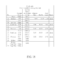
- FIG. 18 shows the optical data of the first example of the optical imaging lens set.
- FIG. 19 shows the aspheric surface data of the first example.
- FIG. 20 shows the optical data of the second example of the optical imaging lens set.
- FIG. 21 shows the aspheric surface data of the second example.
- FIG. 22 shows the optical data of the third example of the optical imaging lens set.
- FIG. 23 shows the aspheric surface data of the third example.
- FIG. 24 shows the optical data of the fourth example of the optical imaging lens set.
- FIG. 25 shows the aspheric surface data of the fourth example.
- FIG. 26 shows the optical data of the fifth example of the optical imaging lens set.
- FIG. 27 shows the aspheric surface data of the fifth example.
- FIG. 28 shows the optical data of the sixth example of the optical imaging lens set.
- FIG. 29 shows the aspheric surface data of the sixth example.
- FIG. 30 shows the optical data of the seventh example of the optical imaging lens set.
- FIG. 31 shows the aspheric surface data of the seventh example.
- FIG. 32 shows some important ratios in the examples.
- a certain lens element has negative/positive refractive power refers to the part in a vicinity of the optical axis of the lens element has negative/positive refractive power.
- An object-side/image-side surface of a certain lens element has a concave/convex part or concave/convex portion refers to the part is more concave/convex in a direction parallel with the optical axis to be compared with an outer region next to the region.
- the optical axis is “I” and the lens element is symmetrical with respect to the optical axis I.
- the object side of the lens element has a convex part in the region A, a concave part in the region B, and a convex part in the region C because region A is more convex in a direction parallel with the optical axis than an outer region (region B) next to region A, region B is more concave than region C and region C is similarly more convex than region E.
- a circular periphery of a certain lens element refers to a circular periphery region of a surface on the lens element for light to pass through, that is, region C in the drawing.
- imaging light includes Lc (chief ray) and Lm (marginal ray).
- a vicinity of the optical axis refers to an optical axis region of a surface on the lens element for light to pass through, that is, the region A in FIG. 15 .
- the lens element may include an extension part E for the lens element to be installed in an optical imaging lens set. Ideally speaking, no light would pass through the extension part, and the actual structure and shape of the extension part is not limited to this and may have other variations. For the reason of simplicity, the extension part is not illustrated in FIGS. 1 , 3 , 5 , 7 , 9 , 11 and 13 .
- the optical imaging lens set 1 of five lens elements of the present invention sequentially from an object side 2 (where an object is located) to an image side 3 along an optical axis 4 , has a first lens element 10 , a second lens element 20 , a third lens element 30 , a fourth lens element 40 , a fifth lens element 50 , a filter 60 and an image plane 71 .
- the first lens element 10 , the second lens element 20 , the third lens element 30 , the fourth lens element 40 and the fifth lens element 50 may be made of a transparent plastic material and each has an appropriate refractive power, but the present invention is not limited to this and the fifth lens element 50 is always made of a transparent plastic material.
- the optical axis 4 is the optical axis of the entire optical imaging lens set 1 , and the optical axis of each of the lens elements coincides with the optical axis of the optical imaging lens set 1 .
- the optical imaging lens set 1 includes an aperture stop (ape. stop) 80 disposed in an appropriate position.
- the aperture stop 80 is disposed between the first lens element 10 and the second lens element 20 .
- an object not shown
- the optical imaging lens set 1 of the present invention forms a clear and sharp image on the image plane 71 at the image side 3 after passing through the first lens element 10 , the aperture stop 80 , the second lens element 20 , the third lens element 30 , the fourth lens element 40 , the fifth lens element 50 and the filter 60 .
- the optional filter 60 may be a filter of various suitable functions, for example, the filter 60 may be an infrared cut filter (IR cut filter), placed between the fifth lens element 50 and the image plane 71 .
- IR cut filter infrared cut filter
- Each lens element in the optical imaging lens set 1 of the present invention has an object-side surface facing toward the object side 2 as well as an image-side surface facing toward the image side 3 .
- each object-side surface and image-side surface in the optical imaging lens set 1 of the present invention has a part in a vicinity of its circular periphery (circular periphery part) away from the optical axis 4 as well as a part in a vicinity of the optical axis (optical axis part) closer to the optical axis 4 .
- the first lens element 10 has an object-side surface 11 and an image-side surface 12 ;
- the second lens element 20 has an object-side surface 21 and an image-side surface 22 ;
- the third lens element 30 has an object-side surface 31 and an image-side surface 32 ;
- the fourth lens element 40 has an object-side surface 41 and an image-side surface 42 ;
- the fifth lens element 50 has an object-side surface 51 and an image-side surface 52 .
- Each lens element in the optical imaging lens set 1 of the present invention further has a central thickness T on the optical axis 4 .
- the first lens element 10 has a first lens element thickness T 1
- the second lens element 20 has a second lens element thickness T 2
- the third lens element 30 has a third lens element thickness T 3
- the fourth lens element 40 has a fourth lens element thickness T 4
- an air gap G is disposed between the first lens element 10 and the second lens element 20
- an air gap G 23 is disposed between the second lens element 20 and the third lens element 30
- an air gap G 34 is disposed between the third lens element 30 and the fourth lens element 40
- FIG. 1 illustrates the first example of the optical imaging lens set 1 of the present invention.
- FIG. 2A for the longitudinal spherical aberration on the image plane 71 of the first example; please refer to FIG. 2B for the astigmatic field aberration on the sagittal direction; please refer to FIG. 2C for the astigmatic field aberration on the tangential direction, and please refer to FIG. 2D for the distortion aberration.
- the Y axis of the spherical aberration in each example is “field of view” for 1.0.
- the Y axis of the astigmatic field and the distortion in each example stands for “image height”.
- the optical imaging lens set 1 of the first example has five lens elements 10 to 50 ; each is made of a plastic material and has refractive power.
- the optical imaging lens set 1 also has a filter 60 , an aperture stop 80 , and an image plane 71 .
- the aperture stop 80 is provided between the first lens element 10 and the second lens element 20 .
- the filter 60 may be an infrared filter (IR cut filter) to prevent inevitable infrared in light reaching the image plane to adversely affect the imaging quality.
- the first lens element 10 has positive refractive power.
- the object-side surface 11 of the first lens element 10 facing toward the object side 2 is a convex surface and the image-side surface 12 of the first lens element 10 facing toward the image side 3 is a concave surface.
- Both the object-side surface 11 and the image-side 12 of the first lens element 10 are aspherical surfaces.
- the second lens element 20 has positive refractive power.
- the object-side surface 21 of the second lens element 20 facing toward the object side 2 is a convex surface and the image-side surface 22 of the second lens element 20 facing toward the image side 3 is a convex surface and has a convex part 27 (convex circular periphery part) in a vicinity of its circular periphery.
- both the object-side surface 21 and the image-side surface 22 of the second lens element 20 are aspherical surfaces.
- the third lens element 30 has positive refractive power, an object-side surface 31 of the third lens element 30 facing toward the object side 2 and an image-side surface 32 of the third lens element 30 facing toward the image side 3 .
- the object-side surface 31 is a concave surface.
- the image-side surface 32 has a convex part 36 (convex optical axis part) in the vicinity of the optical axis and a concave part 37 (concave circular periphery part) in a vicinity of its circular periphery.
- both the object-side surface 31 and the mage-side surface 32 of the third lens element 30 are aspherical surfaces.
- the fourth lens element 40 has negative refractive power.
- the object-side surface 41 of the fourth lens element 40 facing toward the object side 2 has a convex part 43 (convex optical axis part) in the vicinity of the optical axis and a concave part 44 (concave circular periphery part) in a vicinity of its circular periphery.
- the image-side surface 42 of the fourth lens element 40 facing toward the image side 3 has a concave part 46 (concave optical axis part) in the vicinity of the optical axis and a convex part 47 (convex circular periphery part) in a vicinity of its circular periphery.
- both the object-side surface 41 and the image-side 42 of the fourth lens element 40 are aspherical surfaces.
- the fifth lens element 50 has positive refractive power, an object-side surface 51 of the fifth lens element 50 facing toward the object side 2 and an image-side surface 52 of the fifth lens element 50 facing toward the image side 3 .
- the object-side surface 51 has a convex part 53 (convex optical axis part) in the vicinity of the optical axis and a concave part 54 (concave circular periphery part) in a vicinity of its circular periphery.
- the image-side surface 52 has a concave part 56 (concave optical axis part) in the vicinity of the optical axis and a convex part 57 (convex circular periphery part) in a vicinity of its circular periphery. Further, both the object-side surface 51 and the image-side 52 of the fifth lens element 50 are aspherical surfaces.
- the filter 60 may be an infrared cut filter, and is disposed between the fifth lens element 50 and the image plane 71 .
- the object side 11 / 21 / 31 / 41 / 51 and image side 12 / 22 / 32 / 42 / 52 from the first lens element 10 to the fifth lens element 50 , total of ten surfaces are all aspherical.
- These aspheric coefficients are defined according to the following formula:
- R represents the curvature radius of the lens element surface
- Z represents the depth of an aspherical surface (the perpendicular distance between the point of the aspherical surface at a distance Y from the optical axis and the tangent plane of the vertex on the optical axis of the aspherical surface);
- Y represents a vertical distance from a point on the aspherical surface to the optical axis
- K is a conic constant
- a 21 is the aspheric coefficient of the 2i order.
- the optical data of the first example of the optical imaging lens set 1 are shown in FIG. 18 and the Abbe No. is the Abbe number while the aspheric surface data are shown in FIG. 19 .
- the f-number of the entire optical lens element system is Fno
- HFOV stands for the half field of view which is half of the field of view of the entire optical lens element system
- the unit for the curvature radius is in millimeters (mm)
- F is a system focal length Efl of the optical imaging lens set 1 .
- the length of the optical imaging lens set is 3.78 mm (from the first object-side surface to the image plane along the optical axis).
- the image height is 2.268 mm.
- V D2 ⁇ V D1 32.586
- FIG. 3 illustrates the second example of the optical imaging lens set 1 of the present invention.
- FIG. 4A for the longitudinal spherical aberration on the image plane 71 of the second example; please refer to FIG. 4B for the astigmatic aberration on the sagittal direction; please refer to FIG. 4C for the astigmatic aberration on the tangential direction, and please refer to FIG. 4D for the distortion aberration.
- the second example is similar with the first example, but the optical data, the object-side surface 21 , the image-side surface 32 are different.
- the object-side surface 21 of the second lens element 20 is a concave surface and the image-side surface 32 of the third lens element 30 is a convex surface.
- the optical data of the second example of the optical imaging lens set are shown in FIG. 20 while the aspheric surface data are shown in FIG. 21 .
- the length of the optical imaging lens set is 4.17 mm.
- the image height is 2.268 mm.
- V D2 ⁇ V D1 32.586
- FIG. 5 illustrates the third example of the optical imaging lens set 1 of the present invention.
- FIG. 6A for the longitudinal spherical aberration on the image plane 71 of the second example; please refer to FIG. 6B for the astigmatic aberration on the sagittal direction; please refer to FIG. 6C for the astigmatic aberration on the tangential direction, and please refer to FIG. 6D for the distortion aberration.
- the third example is similar with the first example, but the optical data, the object-side surface 21 , and the image-side surface 32 are different,
- the object-side surface 21 of the second lens element 20 has a convex part 23 (convex optical axis part) in the vicinity of the optical axis and a concave part 24 (concave circular periphery part) in a vicinity of its circular periphery and the image-side surface 32 of the third lens element 30 is a convex surface.
- the optical data of the third example of the optical imaging lens set are shown in FIG. 22 while the aspheric surface data are shown in FIG. 23 .
- the length of the optical imaging lens set is 4.04 mm.
- the image height is 2.268 mm.
- V D2 ⁇ V D1 32.586
- FIG. 7 illustrates the fourth example of the optical imaging lens set 1 of the present invention.
- FIG. 8A for the longitudinal spherical aberration on the image plane 71 of the second example; please refer to FIG. 8B for the astigmatic aberration on the sagittal direction; please refer to FIG. 8C for the astigmatic aberration on the tangential direction, and please refer to FIG. 8D for the distortion aberration.
- the fourth example is similar with the first example, but the optical data, the object-side surface 21 , the image-side surface 32 are different.
- the object-side surface 21 of the second lens element 20 has a convex part 23 (convex optical axis part) in the vicinity of the optical axis and a concave part 24 (concave circular periphery part) in a vicinity of its circular periphery and the image-side surface 32 of the third lens element is a convex surface.
- the optical data of the fourth example of the optical imaging lens set are shown in FIG. 24 while the aspheric surface data are shown in FIG. 25 .
- the length of the optical imaging lens set is 4.04 mm.
- the image height is 2.268 mm.
- V D2 ⁇ V D1 32.586
- FIG. 9 illustrates the fifth example of the optical imaging lens set 1 of the present invention.
- FIG. 10A for the longitudinal spherical aberration on the image plane 71 of the second example; please refer to FIG. 10B for the astigmatic aberration on the sagittal direction; please refer to FIG. 10C for the astigmatic aberration on the tangential direction, and please refer to FIG. 10D for the distortion aberration.
- the fifth example is similar with the first example, but the optical data and the image-side surface 32 are different.
- the image-side surface 32 of the third lens element 30 is a convex surface.
- the optical data of the fifth example of the optical imaging lens set are shown in FIG. 26 while the aspheric surface data are shown in FIG. 27 .
- the length of the optical imaging lens set is 4.04 mm.
- the image height is 2.268 mm.
- V D2 ⁇ V D1 32.586
- FIG. 11 illustrates the sixth example of the optical imaging lens set 1 of the present invention.
- FIG. 12A for the longitudinal spherical aberration on the image plane 71 of the second example; please refer to FIG. 12B for the astigmatic aberration on the sagittal direction; please refer to FIG. 12C for the astigmatic aberration on the tangential direction, and please refer to FIG. 12D for the distortion aberration.
- the sixth example is similar with the first example, but the optical data and the image-side surface 32 are different.
- the image-side surface 32 of the third lens element 30 is a convex surface.
- the optical data of the sixth example of the optical imaging lens set are shown in FIG. 28 while the aspheric surface data are shown in FIG. 29 .
- the length of the optical imaging lens set is 3.74 mm.
- the image height is 2.268 mm.
- V D2 ⁇ V D1 32.586
- FIG. 13 illustrates the seventh example of the optical imaging lens set 1 of the present invention.
- FIG. 14A for the longitudinal spherical aberration on the image plane 71 of the second example; please refer to FIG. 14B for the astigmatic aberration on the sagittal direction; please refer to FIG. 14C for the astigmatic aberration on the tangential direction, and please refer to FIG. 14D for the distortion aberration.
- the seventh example is similar with the first example, but the optical data, refractive power of the first lens element 10 , the object-side surface 21 and the image-side surface 32 are different.
- the first lens element 10 has negative refractive power
- the object-side surface 21 of the second lens element 20 has a convex part 23 (convex optical axis part) in the vicinity of the optical axis and a concave part 24 (concave circular periphery part) in a vicinity of its circular periphery
- the image-side surface 32 of the third lens element 30 is a convex surface.
- the optical data of the seventh example of the optical imaging lens set are shown in FIG. 30 while the aspheric surface data are shown in FIG. 31 .
- the length of the optical imaging lens set is 3.89 mm.
- the image height is 2.268 mm.
- V D2 ⁇ V D1 32.586
- the convex circular periphery part of the image-side surface of the second lens element and the concave optical axis part as well as the convex circular periphery part of the fourth image-side surface of the fourth lens element work together to minimize the aberrations.
- the plastic fifth lens element facilitates the reduction of the production cost and the reduction of the weight of the optical imaging lens set.
- T 4 /G 12 should be not greater than 2.0. When the optical imaging lens set is smaller, the total length should be shorter as well. However, because the concave optical axis part of the image-side surface of the fourth lens element, it may be thinner to satisfy this relationship. It is suggested that 0.1 ⁇ T 4 /G 12 ⁇ 2.0. 2.
- E fl /T 2 should be not greater than 7.0. When the optical imaging lens set is shorter, the focal length should be shorter as well to satisfy this relationship. Preferably, it is 3.0 ⁇ E fl /T 2 ⁇ 7.0. A smaller T 2 helps to optimize a better arrange of other lens thickness and gaps when the optical imaging lens set becomes shorter. Or, it is 2.0 ⁇ E fl /T 2 ⁇ 7.0. 3.
- T 2 /T 4 should be not less than 1.4.
- the total length should be shorter as well.
- the concave optical axis part of the image-side surface of the fourth lens element it may be thinner to satisfy this relationship. It is suggested that 1.4 ⁇ T 2 /T 4 ⁇ 3.5.
- T 1 /G 12 should be not greater than 2.5.
- the optical imaging lens set is smaller, the total length should be shorter as well.
- this relationship suggests better results.
- it is 0.5 ⁇ T 1 /G 12 ⁇ 2.5.
- T max /G 12 should be between 0.7 and 2.3.
- T max /T 2 should be not greater than 1.4. When the optical imaging lens set is smaller, the total length should be shorter and the largest thickness should become smaller as well to satisfy this relationship. Preferably, It is suggested that 0.8 ⁇ T max /T 2 ⁇ 1.4. 7. G aa /T 1 should be between 1.5 and 4.0. When the optical imaging lens set is smaller, the total length should be shorter as well. When the optical performance and the productivity are taken into consideration, this relationship suggests better results. 8. T 1 /T 2 should be not greater than 1.1. When the optical imaging lens set is smaller, the total length should be shorter as well.
- V D2 ⁇ V D1 should be not less than 30. Abbe Number is used to evaluate the dispersion properties of a lens. A shortened lens set would have worse dispersion properties. This relationship facilitates to reduce the dispersion properties. Preferably, It is suggested that 30 ⁇ V D2 ⁇ V D1 ⁇ 36.
- the optical imaging lens set 1 of the present invention may be applied to a portable electronic device. Please refer to FIG. 16 .
- FIG. 16 illustrates a first preferred example of the optical imaging lens set 1 of the present invention for use in a portable electronic device 100 .
- the portable electronic device 100 includes a case 110 , and an image module 120 mounted in the case 110 .
- a mobile phone is illustrated in FIG. 16 as an example, but the portable electronic device 100 is not limited to a mobile phone.
- the image module 120 includes the optical imaging lens set 1 as described above.
- FIG. 16 illustrates the aforementioned first example of the optical imaging lens set 1 .
- the portable electronic device 100 also contains a barrel 130 for the installation of the optical imaging lens set 1 , a module housing unit 140 for the installation of the barrel 130 , a substrate 172 for the installation of the module housing unit 140 and an image sensor 70 disposed at the substrate 172 , and at the image side 3 of the optical imaging lens set 1 .
- the image sensor 70 in the optical imaging lens set 1 may be an electronic photosensitive element, such as a charge coupled device or a complementary metal oxide semiconductor element.
- the image plane 71 forms at the image sensor 70 .
- the image sensor 70 used here is a product of chip on board (COB) package rather than a product of the conventional chip scale package (CSP) so it is directly attached to the substrate 172 , and protective glass is not needed in front of the image sensor 70 in the optical imaging lens set 1 , but the present invention is not limited to this.
- COB chip on board
- CSP conventional chip scale package
- the optional filter 60 may be omitted in other examples although the optional filter 60 is present in this example.
- the case 110 , the barrel 130 , and/or the module housing unit 140 may be a single element or consist of a plurality of elements, but the present invention is not limited to this.
- Each one of the five lens elements 10 , 20 , 30 , 40 and 50 with refractive power is installed in the barrel 130 with air gaps disposed between two adjacent lens elements in an exemplary way.
- the module housing unit 140 has a lens element housing 141 , and an image sensor housing 146 installed between the lens element housing 141 and the image sensor 70 .
- the image sensor housing 146 is optional.
- the barrel 130 is installed coaxially along with the lens element housing 141 along the axis I-I′, and the barrel 130 is provided inside of the lens element housing 141 .
- the optical imaging lens set 1 of the present invention may be as short as 3.78 mm, this ideal length allows the dimensions and the size of the portable electronic device 100 to be smaller and lighter, but excellent optical performance and image quality are still possible. In such a way, the various examples of the present invention satisfy the need for economic benefits of using less raw materials in addition to satisfy the trend for a smaller and lighter product design and consumers' demands.
- the lens element housing 141 has a first seat element 142 , a second seat element 143 , a coil 144 and a magnetic component 145 .
- the first seat element 142 is for the installation of the barrel 130 , exteriorly attached to the barrel 130 and disposed along the axis I-I′.
- the second seat element 143 is disposed along the axis I-I′ and surrounds the exterior of the first seat element 142 .
- the coil 144 is provided between the outside of the first seat element 142 and the inside of the second seat element 143 .
- the magnetic component 145 is disposed between the outside of the coil 144 and the inside of the second seat element 143 .
- the first seat element 142 may pull the barrel 130 and the optical imaging lens set 1 which is disposed inside of the barrel 130 to move along the axis I-I′, namely the optical axis 4 in FIG. 1 .
- the image sensor housing 146 is attached to the second seat element 143 .
- the filter 60 such as an infrared filter, is installed at the image sensor housing 146 .
- Other details of the portable electronic device 200 in the second preferred example are similar to those of the portable electronic device 100 in the first preferred example so they are not elaborated again.
Landscapes
- Physics & Mathematics (AREA)
- General Physics & Mathematics (AREA)
- Optics & Photonics (AREA)
- Engineering & Computer Science (AREA)
- Multimedia (AREA)
- Signal Processing (AREA)
- Lenses (AREA)
Abstract
Description
2) The plastic fifth lens element facilitates the reduction of the production cost and the reduction of the weight of the optical imaging lens set.
2. Efl/T2 should be not greater than 7.0. When the optical imaging lens set is shorter, the focal length should be shorter as well to satisfy this relationship. Preferably, it is 3.0≦Efl/T2≦7.0. A smaller T2 helps to optimize a better arrange of other lens thickness and gaps when the optical imaging lens set becomes shorter. Or, it is 2.0≦Efl/T2≦7.0.
3. T2/T4 should be not less than 1.4. When the optical imaging lens set is smaller, the total length should be shorter as well. However, because the concave optical axis part of the image-side surface of the fourth lens element, it may be thinner to satisfy this relationship. It is suggested that 1.4≦T2/T4≦3.5.
4. T1/G12 should be not greater than 2.5. When the optical imaging lens set is smaller, the total length should be shorter as well. When the optical performance and the productivity are taken into consideration, this relationship suggests better results. Preferably, it is 0.5≦T1/G12≦2.5.
5. Tmax/G12 should be between 0.7 and 2.3. When the optical imaging lens set is smaller, the total length should be shorter and the largest thickness should become smaller as well to satisfy this relationship.
6. Tmax/T2 should be not greater than 1.4. When the optical imaging lens set is smaller, the total length should be shorter and the largest thickness should become smaller as well to satisfy this relationship. Preferably, It is suggested that 0.8≦Tmax/T2≦1.4.
7. Gaa/T1 should be between 1.5 and 4.0. When the optical imaging lens set is smaller, the total length should be shorter as well. When the optical performance and the productivity are taken into consideration, this relationship suggests better results.
8. T1/T2 should be not greater than 1.1. When the optical imaging lens set is smaller, the total length should be shorter as well. When the optical performance and the productivity are taken into consideration, this relationship suggests better results. Preferably, It is suggested that 0.3≦T1/T2≦1.1.
9. Gaa/T4 should be between 2.0 and 8.0. When the optical imaging lens set is smaller, the total length should be shorter as well. When the optical performance and the productivity are taken into consideration, this relationship suggests better results.
10. VD2−VD1 should be not less than 30. Abbe Number is used to evaluate the dispersion properties of a lens. A shortened lens set would have worse dispersion properties. This relationship facilitates to reduce the dispersion properties. Preferably, It is suggested that 30≦VD2−VD1≦36.
Claims (12)
Priority Applications (1)
| Application Number | Priority Date | Filing Date | Title |
|---|---|---|---|
| US14/798,202 US9638899B2 (en) | 2013-07-10 | 2015-07-13 | Optical imaging lens and electronic device comprising the same |
Applications Claiming Priority (3)
| Application Number | Priority Date | Filing Date | Title |
|---|---|---|---|
| CN201310288528.9A CN103676087B (en) | 2013-07-10 | 2013-07-10 | Optical imaging lens and apply the electronic installation of this camera lens |
| CN201310288528 | 2013-07-10 | ||
| CN201310288528.9 | 2013-07-10 |
Related Child Applications (1)
| Application Number | Title | Priority Date | Filing Date |
|---|---|---|---|
| US14/798,202 Continuation US9638899B2 (en) | 2013-07-10 | 2015-07-13 | Optical imaging lens and electronic device comprising the same |
Publications (2)
| Publication Number | Publication Date |
|---|---|
| US20150015767A1 US20150015767A1 (en) | 2015-01-15 |
| US9279956B2 true US9279956B2 (en) | 2016-03-08 |
Family
ID=50314179
Family Applications (2)
| Application Number | Title | Priority Date | Filing Date |
|---|---|---|---|
| US14/093,533 Expired - Fee Related US9279956B2 (en) | 2013-07-10 | 2013-12-02 | Optical imaging lens and electronic device comprising the same |
| US14/798,202 Expired - Fee Related US9638899B2 (en) | 2013-07-10 | 2015-07-13 | Optical imaging lens and electronic device comprising the same |
Family Applications After (1)
| Application Number | Title | Priority Date | Filing Date |
|---|---|---|---|
| US14/798,202 Expired - Fee Related US9638899B2 (en) | 2013-07-10 | 2015-07-13 | Optical imaging lens and electronic device comprising the same |
Country Status (3)
| Country | Link |
|---|---|
| US (2) | US9279956B2 (en) |
| CN (1) | CN103676087B (en) |
| TW (1) | TWI479222B (en) |
Cited By (1)
| Publication number | Priority date | Publication date | Assignee | Title |
|---|---|---|---|---|
| US12372746B2 (en) | 2022-09-02 | 2025-07-29 | Largan Precision Co., Ltd. | Imaging system lens assembly, image capturing unit and electronic device |
Families Citing this family (9)
| Publication number | Priority date | Publication date | Assignee | Title |
|---|---|---|---|---|
| TWI456248B (en) | 2013-07-23 | 2014-10-11 | Largan Precision Co Ltd | Image lens assembly and image capturing device |
| TWI592681B (en) | 2013-08-02 | 2017-07-21 | 玉晶光電股份有限公司 | Optical imaging lens and the electronic device using the lens |
| CN103676103B (en) * | 2013-08-02 | 2016-04-20 | 玉晶光电(厦门)有限公司 | Optical imaging lens and apply the electronic installation of this camera lens |
| CN106970452B (en) * | 2016-01-13 | 2019-05-07 | 大立光电股份有限公司 | Imaging optical lens assembly, image capturing device and electronic device |
| TWI627467B (en) | 2017-03-22 | 2018-06-21 | 大立光電股份有限公司 | Imaging system lens group, image capturing device and electronic device |
| WO2019024493A1 (en) * | 2017-07-31 | 2019-02-07 | 浙江舜宇光学有限公司 | Imaging lens |
| US12372742B2 (en) | 2020-05-15 | 2025-07-29 | Samsung Electronics Co., Ltd. | Wide-field imaging lens and optical image capturing device for electronic mobile devices |
| CN113253429B (en) * | 2021-06-08 | 2021-09-17 | 江西联益光学有限公司 | Wide-angle lens and imaging apparatus |
| CN116400479A (en) * | 2023-03-09 | 2023-07-07 | 信扬科技(佛山)有限公司 | Lens module and terminal equipment |
Citations (33)
| Publication number | Priority date | Publication date | Assignee | Title |
|---|---|---|---|---|
| JPH04197994A (en) | 1990-11-28 | 1992-07-17 | Hitachi Ltd | Crane saddle unit |
| TW200722785A (en) | 2005-12-02 | 2007-06-16 | Asia Optical Co Inc | Single focus lens |
| JP2008281760A (en) | 2007-05-10 | 2008-11-20 | Ricoh Opt Ind Co Ltd | Photographic lens and photographic device |
| JP4197994B2 (en) | 2003-06-19 | 2008-12-17 | コニカミノルタオプト株式会社 | Imaging device |
| US7480105B2 (en) | 2006-04-05 | 2009-01-20 | Fujinon Corporation | Imaging lens and imaging apparatus |
| TWM369459U (en) | 2009-04-07 | 2009-11-21 | Fujinon Corp | Photographic lens and photographing apparatus |
| JP2009294528A (en) | 2008-06-06 | 2009-12-17 | Fujinon Corp | Imaging lens composed of five lenses and imaging apparatus |
| TW201022714A (en) | 2008-12-01 | 2010-06-16 | Largan Precision Co Ltd | Optical lens system for taking image |
| JP2010224521A (en) | 2009-02-27 | 2010-10-07 | Konica Minolta Opto Inc | Imaging lens, imaging device, and mobile terminal |
| US20100254029A1 (en) | 2009-04-07 | 2010-10-07 | Yoshikazu Shinohara | Imaging lens, imaging apparatus and portable terminal device |
| US7911712B2 (en) | 2008-10-29 | 2011-03-22 | Fujinon Corporation | Imaging lens and imaging apparatus |
| US20110176049A1 (en) * | 2010-01-19 | 2011-07-21 | Largan Precision Co., Ltd. | Optical photographing lens assembly |
| TW201137430A (en) | 2010-04-23 | 2011-11-01 | Largan Precision Co Ltd | Photographing optical lens assembly |
| US20110316969A1 (en) | 2010-06-28 | 2011-12-29 | Largan Precision Co., Ltd. | Wide-viewing-angle imaging lens assembly |
| JP4858648B2 (en) | 2008-08-25 | 2012-01-18 | コニカミノルタオプト株式会社 | Imaging lens, imaging device, and portable terminal |
| US20120092544A1 (en) | 2009-06-12 | 2012-04-19 | Largan Precision Co., Ltd. | Imaging lens assembly |
| US8179614B1 (en) | 2011-01-03 | 2012-05-15 | Largan Precision Co. | Image pickup optical lens assembly |
| US20120147482A1 (en) | 2010-12-09 | 2012-06-14 | Largan Precision Co. | Image Pickup Optical System |
| US20120154929A1 (en) | 2010-12-15 | 2012-06-21 | Largan Precision Co. | Imagery Optical System |
| US20120218647A1 (en) | 2011-02-28 | 2012-08-30 | Kantatsu Co., Ltd. | Imaging lens unit |
| US8284291B2 (en) | 2010-11-01 | 2012-10-09 | Largan Precision Co., Ltd. | Photographing optical lens assembly |
| US20120262806A1 (en) | 2011-04-13 | 2012-10-18 | Largan Precision Co., Ltd. | Optical image lens assembly |
| JP2012211933A (en) | 2011-03-30 | 2012-11-01 | Fujifilm Corp | Imaging lens and imaging apparatus |
| US8325429B2 (en) | 2010-12-23 | 2012-12-04 | Largan Precision Co., Ltd. | Photographing optical lens assembly |
| US8334922B2 (en) | 2009-04-07 | 2012-12-18 | Fujifilm Corporation | Imaging lens, imaging apparatus and portable terminal device |
| US8345323B2 (en) | 2009-06-25 | 2013-01-01 | Fujifilm Corporation | Image reading lens system and image reading apparatus |
| US20130010374A1 (en) | 2011-07-06 | 2013-01-10 | Largan Precision Co., Ltd. | Image capturing optical system |
| US20130021680A1 (en) | 2011-07-19 | 2013-01-24 | Largan Precision Co., Ltd. | Optical image capturing lens system |
| US20130050847A1 (en) | 2011-08-26 | 2013-02-28 | Largan Precision Co., Ltd. | Image lens assembly |
| US20130057967A1 (en) | 2011-09-02 | 2013-03-07 | Largan Precision Co., Ltd. | Photographing optical lens assembly |
| US20130107376A1 (en) | 2011-10-27 | 2013-05-02 | Largan Precision Co., Ltd | Image lens assembly |
| TW201321830A (en) | 2012-11-02 | 2013-06-01 | 玉晶光電股份有限公司 | Mobile device and optical imaging lens thereof |
| US8908289B2 (en) * | 2011-03-30 | 2014-12-09 | Fujifilm Corporation | Image capturing lens and image capturing apparatus |
Family Cites Families (6)
| Publication number | Priority date | Publication date | Assignee | Title |
|---|---|---|---|---|
| US7663813B2 (en) * | 2008-01-02 | 2010-02-16 | Newmax Technology Co., Ltd. | Imaging lens module |
| TWI432773B (en) * | 2009-04-20 | 2014-04-01 | Largan Precision Co Ltd | Photographing lens assembly |
| US8559118B2 (en) * | 2009-11-18 | 2013-10-15 | DigitalOptics Corporation Europe Limited | Fixed focal length optical lens architecture providing a customized depth of focus optical system |
| TWI474072B (en) * | 2012-06-14 | 2015-02-21 | Largan Precision Co Ltd | Optical image lens system |
| TWI463168B (en) * | 2013-05-30 | 2014-12-01 | Largan Precision Co Ltd | Imaging lens system and image capturing device |
| TWI456248B (en) * | 2013-07-23 | 2014-10-11 | Largan Precision Co Ltd | Image lens assembly and image capturing device |
-
2013
- 2013-07-10 CN CN201310288528.9A patent/CN103676087B/en active Active
- 2013-08-09 TW TW102128704A patent/TWI479222B/en not_active IP Right Cessation
- 2013-12-02 US US14/093,533 patent/US9279956B2/en not_active Expired - Fee Related
-
2015
- 2015-07-13 US US14/798,202 patent/US9638899B2/en not_active Expired - Fee Related
Patent Citations (37)
| Publication number | Priority date | Publication date | Assignee | Title |
|---|---|---|---|---|
| JPH04197994A (en) | 1990-11-28 | 1992-07-17 | Hitachi Ltd | Crane saddle unit |
| JP4197994B2 (en) | 2003-06-19 | 2008-12-17 | コニカミノルタオプト株式会社 | Imaging device |
| TW200722785A (en) | 2005-12-02 | 2007-06-16 | Asia Optical Co Inc | Single focus lens |
| US7480105B2 (en) | 2006-04-05 | 2009-01-20 | Fujinon Corporation | Imaging lens and imaging apparatus |
| CN100555021C (en) | 2006-04-05 | 2009-10-28 | 富士能株式会社 | Imaging lens system and camera head |
| JP2008281760A (en) | 2007-05-10 | 2008-11-20 | Ricoh Opt Ind Co Ltd | Photographic lens and photographic device |
| JP5052956B2 (en) | 2007-05-10 | 2012-10-17 | リコー光学株式会社 | Photographing lens and photographing device |
| JP2009294528A (en) | 2008-06-06 | 2009-12-17 | Fujinon Corp | Imaging lens composed of five lenses and imaging apparatus |
| JP4858648B2 (en) | 2008-08-25 | 2012-01-18 | コニカミノルタオプト株式会社 | Imaging lens, imaging device, and portable terminal |
| US7911712B2 (en) | 2008-10-29 | 2011-03-22 | Fujinon Corporation | Imaging lens and imaging apparatus |
| TW201022714A (en) | 2008-12-01 | 2010-06-16 | Largan Precision Co Ltd | Optical lens system for taking image |
| JP2010224521A (en) | 2009-02-27 | 2010-10-07 | Konica Minolta Opto Inc | Imaging lens, imaging device, and mobile terminal |
| US8334922B2 (en) | 2009-04-07 | 2012-12-18 | Fujifilm Corporation | Imaging lens, imaging apparatus and portable terminal device |
| TWM369459U (en) | 2009-04-07 | 2009-11-21 | Fujinon Corp | Photographic lens and photographing apparatus |
| US8390941B2 (en) | 2009-04-07 | 2013-03-05 | Fujinon Corporation | Imaging lens, imaging apparatus and portable terminal device |
| US20100254029A1 (en) | 2009-04-07 | 2010-10-07 | Yoshikazu Shinohara | Imaging lens, imaging apparatus and portable terminal device |
| US20120092544A1 (en) | 2009-06-12 | 2012-04-19 | Largan Precision Co., Ltd. | Imaging lens assembly |
| US8345323B2 (en) | 2009-06-25 | 2013-01-01 | Fujifilm Corporation | Image reading lens system and image reading apparatus |
| US20110176049A1 (en) * | 2010-01-19 | 2011-07-21 | Largan Precision Co., Ltd. | Optical photographing lens assembly |
| US8248713B2 (en) | 2010-01-19 | 2012-08-21 | Largan Precision Co., Ltd. | Optical photographing lens assembly |
| TW201137430A (en) | 2010-04-23 | 2011-11-01 | Largan Precision Co Ltd | Photographing optical lens assembly |
| US20110316969A1 (en) | 2010-06-28 | 2011-12-29 | Largan Precision Co., Ltd. | Wide-viewing-angle imaging lens assembly |
| US8284291B2 (en) | 2010-11-01 | 2012-10-09 | Largan Precision Co., Ltd. | Photographing optical lens assembly |
| US20120147482A1 (en) | 2010-12-09 | 2012-06-14 | Largan Precision Co. | Image Pickup Optical System |
| US20120154929A1 (en) | 2010-12-15 | 2012-06-21 | Largan Precision Co. | Imagery Optical System |
| US8325429B2 (en) | 2010-12-23 | 2012-12-04 | Largan Precision Co., Ltd. | Photographing optical lens assembly |
| US8179614B1 (en) | 2011-01-03 | 2012-05-15 | Largan Precision Co. | Image pickup optical lens assembly |
| US20120218647A1 (en) | 2011-02-28 | 2012-08-30 | Kantatsu Co., Ltd. | Imaging lens unit |
| JP2012211933A (en) | 2011-03-30 | 2012-11-01 | Fujifilm Corp | Imaging lens and imaging apparatus |
| US8908289B2 (en) * | 2011-03-30 | 2014-12-09 | Fujifilm Corporation | Image capturing lens and image capturing apparatus |
| US20120262806A1 (en) | 2011-04-13 | 2012-10-18 | Largan Precision Co., Ltd. | Optical image lens assembly |
| US20130010374A1 (en) | 2011-07-06 | 2013-01-10 | Largan Precision Co., Ltd. | Image capturing optical system |
| US20130021680A1 (en) | 2011-07-19 | 2013-01-24 | Largan Precision Co., Ltd. | Optical image capturing lens system |
| US20130050847A1 (en) | 2011-08-26 | 2013-02-28 | Largan Precision Co., Ltd. | Image lens assembly |
| US20130057967A1 (en) | 2011-09-02 | 2013-03-07 | Largan Precision Co., Ltd. | Photographing optical lens assembly |
| US20130107376A1 (en) | 2011-10-27 | 2013-05-02 | Largan Precision Co., Ltd | Image lens assembly |
| TW201321830A (en) | 2012-11-02 | 2013-06-01 | 玉晶光電股份有限公司 | Mobile device and optical imaging lens thereof |
Cited By (1)
| Publication number | Priority date | Publication date | Assignee | Title |
|---|---|---|---|---|
| US12372746B2 (en) | 2022-09-02 | 2025-07-29 | Largan Precision Co., Ltd. | Imaging system lens assembly, image capturing unit and electronic device |
Also Published As
| Publication number | Publication date |
|---|---|
| US20150015767A1 (en) | 2015-01-15 |
| TW201411222A (en) | 2014-03-16 |
| CN103676087B (en) | 2015-12-09 |
| US20160187624A1 (en) | 2016-06-30 |
| TWI479222B (en) | 2015-04-01 |
| CN103676087A (en) | 2014-03-26 |
| US9638899B2 (en) | 2017-05-02 |
Similar Documents
| Publication | Publication Date | Title |
|---|---|---|
| US11740441B2 (en) | Optical imaging lens and electronic device comprising the same | |
| US9036276B2 (en) | Optical imaging lens set and electronic device comprising the same | |
| US9383552B2 (en) | Optical imaging lens and electronic device comprising the same | |
| US9191561B2 (en) | Optical imaging lens and electronic device comprising the same | |
| US9077876B2 (en) | Optical imaging lens set and electronic device comprising the same | |
| US9565344B2 (en) | Optical imaging lens and electronic device comprising the same | |
| US9025258B2 (en) | Optical imaging lens set and electronic device comprising the same | |
| US9075221B2 (en) | Optical imaging lens and electronic device comprising the same | |
| US9279956B2 (en) | Optical imaging lens and electronic device comprising the same | |
| US9535234B2 (en) | Optical imaging lens and electronic device comprising the same | |
| US9465196B2 (en) | Optical imaging lens and electronic device comprising the same | |
| US20150160437A1 (en) | Optical imaging lens and electronic device comprising the same | |
| US9057865B1 (en) | Optical imaging lens and eletronic device comprising the same | |
| US9829678B2 (en) | Optical imaging lens and electronic device comprising the same | |
| US9274318B1 (en) | Optical imaging lens and electronic device comprising the same | |
| US9013813B2 (en) | Optical imaging lens set and electronic device comprising the same | |
| US20150212287A1 (en) | Optical imaging lens and electronic device comprising the same | |
| US9110269B2 (en) | Optical imaging lens and electronic device comprising the same | |
| US20150301309A1 (en) | Optical imaging lens and electronic device comprising the same |
Legal Events
| Date | Code | Title | Description |
|---|---|---|---|
| AS | Assignment |
Owner name: GENIUS ELECTRONIC OPTICAL CO., LTD., TAIWAN Free format text: ASSIGNMENT OF ASSIGNORS INTEREST;ASSIGNORS:LIN, CHIA-CHENG;FAN, TA-CHENG;REEL/FRAME:031695/0184 Effective date: 20131124 |
|
| ZAAA | Notice of allowance and fees due |
Free format text: ORIGINAL CODE: NOA |
|
| ZAAB | Notice of allowance mailed |
Free format text: ORIGINAL CODE: MN/=. |
|
| ZAAA | Notice of allowance and fees due |
Free format text: ORIGINAL CODE: NOA |
|
| ZAAB | Notice of allowance mailed |
Free format text: ORIGINAL CODE: MN/=. |
|
| STCF | Information on status: patent grant |
Free format text: PATENTED CASE |
|
| MAFP | Maintenance fee payment |
Free format text: PAYMENT OF MAINTENANCE FEE, 4TH YEAR, LARGE ENTITY (ORIGINAL EVENT CODE: M1551); ENTITY STATUS OF PATENT OWNER: LARGE ENTITY Year of fee payment: 4 |
|
| FEPP | Fee payment procedure |
Free format text: MAINTENANCE FEE REMINDER MAILED (ORIGINAL EVENT CODE: REM.); ENTITY STATUS OF PATENT OWNER: LARGE ENTITY |
|
| LAPS | Lapse for failure to pay maintenance fees |
Free format text: PATENT EXPIRED FOR FAILURE TO PAY MAINTENANCE FEES (ORIGINAL EVENT CODE: EXP.); ENTITY STATUS OF PATENT OWNER: LARGE ENTITY |
|
| STCH | Information on status: patent discontinuation |
Free format text: PATENT EXPIRED DUE TO NONPAYMENT OF MAINTENANCE FEES UNDER 37 CFR 1.362 |
|
| FP | Lapsed due to failure to pay maintenance fee |
Effective date: 20240308 |