US9269857B2 - Method and system for eliminating yellow ring occurring on white light emitting diode - Google Patents
Method and system for eliminating yellow ring occurring on white light emitting diode Download PDFInfo
- Publication number
- US9269857B2 US9269857B2 US14/060,593 US201314060593A US9269857B2 US 9269857 B2 US9269857 B2 US 9269857B2 US 201314060593 A US201314060593 A US 201314060593A US 9269857 B2 US9269857 B2 US 9269857B2
- Authority
- US
- United States
- Prior art keywords
- lightspot
- yellow ring
- look
- atomization
- unit
- Prior art date
- Legal status (The legal status is an assumption and is not a legal conclusion. Google has not performed a legal analysis and makes no representation as to the accuracy of the status listed.)
- Expired - Fee Related, expires
Links
- 238000000034 method Methods 0.000 title claims abstract description 106
- 238000000889 atomisation Methods 0.000 claims abstract description 95
- 230000008569 process Effects 0.000 claims abstract description 60
- 238000004806 packaging method and process Methods 0.000 claims abstract description 51
- OAICVXFJPJFONN-UHFFFAOYSA-N Phosphorus Chemical compound [P] OAICVXFJPJFONN-UHFFFAOYSA-N 0.000 claims abstract description 23
- 239000000843 powder Substances 0.000 claims abstract description 20
- 230000009471 action Effects 0.000 claims description 35
- 238000002474 experimental method Methods 0.000 claims description 7
- 230000008030 elimination Effects 0.000 abstract description 16
- 238000003379 elimination reaction Methods 0.000 abstract description 16
- 238000010191 image analysis Methods 0.000 abstract description 3
- 238000010586 diagram Methods 0.000 description 6
- 230000008901 benefit Effects 0.000 description 5
- 230000003287 optical effect Effects 0.000 description 5
- 230000000694 effects Effects 0.000 description 3
- 238000000149 argon plasma sintering Methods 0.000 description 2
- 238000005286 illumination Methods 0.000 description 2
- 238000012986 modification Methods 0.000 description 2
- 230000004048 modification Effects 0.000 description 2
- 239000000919 ceramic Substances 0.000 description 1
- 239000011248 coating agent Substances 0.000 description 1
- 238000000576 coating method Methods 0.000 description 1
- 150000001875 compounds Chemical class 0.000 description 1
- 238000013461 design Methods 0.000 description 1
- 238000005516 engineering process Methods 0.000 description 1
- 239000000203 mixture Substances 0.000 description 1
- 230000009467 reduction Effects 0.000 description 1
- 238000009517 secondary packaging Methods 0.000 description 1
- 238000013519 translation Methods 0.000 description 1
- 230000014616 translation Effects 0.000 description 1
Images


Classifications
-
- H01L33/0095—
-
- H—ELECTRICITY
- H10—SEMICONDUCTOR DEVICES; ELECTRIC SOLID-STATE DEVICES NOT OTHERWISE PROVIDED FOR
- H10H—INORGANIC LIGHT-EMITTING SEMICONDUCTOR DEVICES HAVING POTENTIAL BARRIERS
- H10H20/00—Individual inorganic light-emitting semiconductor devices having potential barriers, e.g. light-emitting diodes [LED]
- H10H20/01—Manufacture or treatment
-
- B—PERFORMING OPERATIONS; TRANSPORTING
- B23—MACHINE TOOLS; METAL-WORKING NOT OTHERWISE PROVIDED FOR
- B23K—SOLDERING OR UNSOLDERING; WELDING; CLADDING OR PLATING BY SOLDERING OR WELDING; CUTTING BY APPLYING HEAT LOCALLY, e.g. FLAME CUTTING; WORKING BY LASER BEAM
- B23K26/00—Working by laser beam, e.g. welding, cutting or boring
- B23K26/02—Positioning or observing the workpiece, e.g. with respect to the point of impact; Aligning, aiming or focusing the laser beam
- B23K26/03—Observing, e.g. monitoring, the workpiece
- B23K26/032—Observing, e.g. monitoring, the workpiece using optical means
-
- B—PERFORMING OPERATIONS; TRANSPORTING
- B23—MACHINE TOOLS; METAL-WORKING NOT OTHERWISE PROVIDED FOR
- B23K—SOLDERING OR UNSOLDERING; WELDING; CLADDING OR PLATING BY SOLDERING OR WELDING; CUTTING BY APPLYING HEAT LOCALLY, e.g. FLAME CUTTING; WORKING BY LASER BEAM
- B23K26/00—Working by laser beam, e.g. welding, cutting or boring
- B23K26/08—Devices involving relative movement between laser beam and workpiece
- B23K26/082—Scanning systems, i.e. devices involving movement of the laser beam relative to the laser head
-
- H01L2933/0091—
-
- H01L33/54—
-
- H—ELECTRICITY
- H10—SEMICONDUCTOR DEVICES; ELECTRIC SOLID-STATE DEVICES NOT OTHERWISE PROVIDED FOR
- H10H—INORGANIC LIGHT-EMITTING SEMICONDUCTOR DEVICES HAVING POTENTIAL BARRIERS
- H10H20/00—Individual inorganic light-emitting semiconductor devices having potential barriers, e.g. light-emitting diodes [LED]
- H10H20/80—Constructional details
- H10H20/85—Packages
- H10H20/852—Encapsulations
- H10H20/853—Encapsulations characterised by their shape
-
- H—ELECTRICITY
- H10—SEMICONDUCTOR DEVICES; ELECTRIC SOLID-STATE DEVICES NOT OTHERWISE PROVIDED FOR
- H10H—INORGANIC LIGHT-EMITTING SEMICONDUCTOR DEVICES HAVING POTENTIAL BARRIERS
- H10H20/00—Individual inorganic light-emitting semiconductor devices having potential barriers, e.g. light-emitting diodes [LED]
- H10H20/80—Constructional details
- H10H20/882—Scattering means
Definitions
- the present invention relates to an elimination technique of yellow ring occurring on a white light emitting diode (LED). Particularly, the present invention relates to a method and system for eliminating yellow ring occurring on the white LED having a blue light chip exciting yellow phosphor powders and having a packaging surface enclosing thereon.
- LED white light emitting diode
- LEDs Light emitting diodes
- a LED is presented by employing the policy of a mixture of light emitting from a red, green and blue light chip, a blue light chip exciting red and green phosphor powders, and a blue chip exciting yellow phosphor powders, respectively.
- the structure of using a blue light chip and yellow phosphor is the most attractive one owing to its simple and cost saving.
- LED packaging structure in which a phosphor layer is provided for a white light with the phosphor powders contained therein arranged in a particular pattern for reduction of the yellow ring phenomenon.
- Another solution taught a LED optical lens, where a lens body is provided to have a particular design so that uniformity of the LED illumination arrangement and angle is improved.
- a LED packaging structure capable of wide angle and uniform outputting light, in such a manner that the light attenuation issue and secondary packaging issue may be improved and eliminated, respectively.
- a LED based lamp in which a lens and microlenses each being in a polygonal shape are provided so that the emitted light may be directed to the microlenses through the lens to achieve good light scattering effect.
- Another solution suggested a LED assembly, where a filter layer is provided to let the LED light with a particular wavelength at least partially reflected, to reduce the yellow ring phenomenon.
- Another prior art disclosed a LED having at least a porous ceramic element for light scattering.
- a LED with a phosphor coating in which a dye compound is contained to improve the uniformity of the light distribution pattern viewed externally to the device.
- the inventor of this application suggests a method and system for eliminating yellow ring occurring on the white LED having a blue light chip exciting yellow phosphor powders and having a packaging surface enclosing thereon on a lightspot by lightspot basis, which is performed at a place other than within the packaging surface.
- the method of for eliminating a yellow ring phenomenon occurring on a plurality of lightspots of a white light emitting diode (LED) having a blue light chip exciting a plurality of yellow phosphor powders and having a packaging surface thereon comprising steps of: (a) acquiring a lightspot image of a lightspot outside the packaging surface of the white LED; (b) analyzing the lightspot image; (c) looking for a coarse degree required and corresponding to the lightspot image from a look-up table having a relationship between a plurality of lightspot images and a plurality of coarse degrees corresponding thereto; (d) launching an atomization process on the packaging surface of white LED according to the coarse degree corresponding to the lightspot image; (e) determining if the lightspot is a final one among the plurality of lightspots, and going back to step (a) with respect to a next one among the plurality of lightspots if the lightspot is determined as an intermediate lightspot; and (f) ending
- the plurality of lightspot images and the plurality of coarse degree corresponding thereto are all null in the look-up table
- the step (c) further comprises steps of: determining if the lightspot image has the coarse degree corresponding thereto being found or if the lightspot image is new to the look-up table; continuing the method to the step (d) if the lightspot image is found with the coarse degree corresponding thereto; launching a single atomization action on the lightspot if the lightspot image is new to the look-up table and recording the coarse degree corresponding to the single atomization; going back to the step (b) if the lightspot image is still new to the look-up table; performing the step (d) if the lightspot image is found with the coarse degree corresponding thereto and recording the lightspot image and a total coarse degree accumulated from the one or more times of single atomization actions as performed as a relationship pair into the look-up table.
- the method further comprises a step (al) before the step (a) of: launching a pre-atomization action on the lightspot equivalent to the lightspot in the step (a).
- the step (b) further comprises steps of: acquiring an intensity of each of a plurality of dots in the lightspot image; and calculating the intensity of each of the plurality of points in the lightspot image as a first yellow ring index; and the step (c) further comprises a step of looking for the coarse degree required and corresponding to the yellow ring information including the first yellow ring index from the look-up table.
- step (b) further comprises a step of acquiring a width of the yellow ring information as a second yellow ring index; and the step (d) further comprises a step of launching the atomization process according to the coarse degree corresponding to the yellow ring information including the second yellow ring index.
- the analyzing unit further comprises a width acquiring unit, acquiring a width of the lightspot image as an atomization width; and the atomization process unit further comprises a width-based atomization process unit, launching the atomization process according to the coarse degree corresponding to the lightspot image and the atomization width.
- the atomization action and process are each enabled by a laser, and the coarse degree associated with the atomization action is adjustable by controlling a scanning speed and energy of the laser.
- the laser has a focusing point controlled by a stepping motor.
- the look-up table is established based on an experiment process.
- the system for eliminating a yellow ring phenomenon occurring on a plurality of lightspots of a white light emitting diode (LED) having a blue light chip exciting a plurality of yellow phosphor powders and having a packaging surface thereon comprises: an image acquiring unit, acquiring a lightspot image of one of the plurality of lightspots outside the packaging surface of the white LED; an analyzing unit, analyzing the lightspot image; a look-up unit, looking for a coarse degree required and corresponding to the lightspot image from a look-up table having a relationship between a plurality of lightspot images and coarse degrees corresponding thereto; an atomization process unit, launching an atomization process on the lightspot according to the coarse degree corresponding to the lightspot image; a final lightspot determination unit, determining if the lightspot is a final one among the plurality of lightspots and directing the image acquiring unit to acquire the lightspot image with respect to a next one among the plurality of lightspots if the lightspot is
- the look-up unit further comprises: a data existing determination unit, determining if the lightspot image has the coarse degree corresponding thereto being found or if the lightspot image is new to the look-up table, and directing the final lightspot determination unit to determine if the lightspot is the final lightspot if the lightspot image is found with the coarse degree corresponding thereto; a single atomization unit, launching a single atomization action on the packaging surface of white LED if the lightspot image is new to the look-up table and recording the coarse degree corresponding to the single atomization, while directing the analyzing unit to analyze the lightspot image if the lightspot image is still new to the look-up table; and an atomization and recording unit, directing the atomization process unit to launch the atomization process if the lightspot image is found with the coarse degree corresponding thereto and recording the lightspot image and a total coarse degree
- system further comprises a pre-atomization action unit for launching a pre-atomization action on the packaging surface of white LED equivalent to the lightspot processed in the image acquiring unit.
- the analyzing unit further comprises a dot intensity acquiring unit, acquiring an intensity of each of a plurality of dots in the-lightspot image, and an intensity calculating unit, calculating the intensity of each of the plurality of dots in the lightspot image as a first yellow ring index; and the look-up unit further comprises an index-based look-up unit, looking for the coarse degree required and corresponding to the yellow ring information having the first yellow ring index from the look-up table.
- the analyzing unit further comprises a width acquiring unit, acquiring a width of the lightspot image as a second yellow ring index; and the atomization process unit further comprises a width-based atomization process unit, launching the atomization process according to the coarse degree corresponding to the yellow ring information including the second lightspot image.
- the atomization action and process are each enabled by a laser, and the coarse degree associated with the atomization action is adjustable by controlling a scanning speed and energy of the laser.
- the laser has a focusing point controlled by a stepping motor.
- the look-up table is established based on an experiment process.
- an advantage of the present invention to provide a method and system for eliminating a yellow ring occurring on a white LED of such kind, which can provide a service for the manufacturers whoever desires to eliminate the yellow ring phenomenon of their white LED products.
- Another advantage of the present invention is to provide a method and system for eliminating a yellow ring occurring on a white LED of such kind, which can have a reduced cost in elimination of the yellow ring phenomenon, as compared to the implementation of the conventional secondary optical elements.
- Yet another advantage of the present invention is to provide a method and system for eliminating a yellow ring occurring on a white LED of such kind, which can be applied onto all kinds of white LED products.
- Still another advantage of the present invention is to provide a method and system for eliminating a yellow ring occurring on a white LED of such kind, which can be guaranteed to take effect in a yellow ring elimination task.
- FIG. 1 is a main process flowchart for describing a method for eliminating yellow ring occurring on a white light emitting diode (LED) having a blue light chip exciting yellow phosphor powders and having a packaging surface enclosing thereon according to the present invention
- LED white light emitting diode
- FIG. 2 is a sub-process flowchart associated with the method as shown in FIG. 1 ;
- FIG. 3 is a sub-process flowchart associated with the method as shown in FIG. 1 ;
- FIG. 4 is a sub-process flowchart associated with the method as shown in FIG. 1 ;
- FIG. 5 is a block diagram for describing a system for eliminating yellow ring occurring on the white LED having the blue light chip exciting the yellow phosphor powders and having a packaging surface enclosing thereon according to the present invention
- FIG. 6 is a schematic diagram of an atomization apparatus used in the present invention.
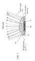
- FIG. 7 is a schematic diagram of the white LED at a lighting state when it has been atomized at the right and left portions of its packaging surface according to the present invention, in which the outgoing light is further mixed at the rough right and left packaging surface portions.
- FIG. 1 a process flowchart for describing a method for eliminating yellow ring occurring on a white light emitting diode (LED) having a blue light chip exciting yellow phosphor powders and having a packaging surface enclosing thereon according to the present invention is shown therein.
- LED white light emitting diode
- the method comprises the following steps and will be described in details below.
- a lightspot image of a lightspot outside the packaging surface of the white LED is acquired (S 110 ) for analyzing the yellow ring phenomenon.
- the yellow ring index for the lightspot is analyzed (S 120 ) and the lightspot image is generated.
- the generated lightspot image may be serving as a reference for recognizing and eliminating the yellow ring, which is right the purpose of the present invention.
- the look-up table has a relationship between a plurality of lightspot images and a plurality of coarse degrees corresponding thereto (S 130 ). That is, a lightspot image has a corresponding coarse degree in the look-up table.
- an atomization process is launched on the packaging surface of white LED according to the coarse degree corresponding to the lightspot image as found in the look-up table (S 140 ).
- the atomization process is enabled by a laser.
- the coarse degree associated with the atomization action is adjustable by controlling a scanning speed and energy of the laser.
- the look-up table is established based on an experiment process with respect to such white LED.
- the method goes back to step S 110 with respect to a next one among the plurality of lightspots.
- the plurality of lightspot images and the plurality of coarse degree corresponding thereto are all null in the look-up table at the first beginning of the method performed.
- the step (S 130 ) further comprises the following steps, which may be referred to FIG. 2 .
- the step (S 140 ) is performed.
- the lightspot image and a total coarse degree accumulated from the one or more times of single atomization actions as performed as a relationship pair are recorded into the look-up table as a future look-up table.
- a step is further comprised before the step (S 110 ). It is to launch a pre-atomization action on the packaging surface of white LED, which is right the lightspot in the step (S 100 ). This is done before a lightspot image with respect to the lightspot is acquired and analyzed, different from that described in the above, in which the atomization process is performed after the lightspot image is acquired and analyzed. But, in some sense, these two policies are equivalent since even a pre-atomization is performed, the yellow ring elimination task still requires a lightspot image analysis process to realize how to be processed with the lightspot on the packaging surface of the white LED, so that the yellow ring may be accurately eliminated.
- step (S 120 ) further comprises the following steps.
- the step (S 130 ) further comprises a step of looking for the coarse degree required and corresponding to the yellow ring information including the first yellow ring index from the look-up table (S 131 ).
- the step (S 140 ) further comprises a step of launching the atomization process according to the coarse degree corresponding to the yellow ring information including the first yellow ring index (S 141 ).
- the lightspot image in the step (S 120 ) further comprises a step of acquiring a width of the lightspot image as a second yellow ring index (S 123 ).
- the step (S 130 ) further comprises a step of looking for the coarse degree required and corresponding to the yellow ring information including the second yellow ring index from the look-up table (S 132 ).
- the step (S 140 ) further comprises a step of launching the atomization process according to the coarse degree corresponding to the yellow ring information including the second yellow ring index (S 142 ).
- the first and second yellow ring indexes are both contained in the yellow ring information.
- the laser can control the obtained coarse degree made by each atomization action by adjusting its scanning speed and energy.
- the look-up table is established in advanced by an experiment process with respect to such white LED.
- FIG. 5 it is a block diagram for describing a system for eliminating yellow ring occurring on the white LED having the blue light chip exciting the yellow phosphor powders and having a packaging surface enclosing thereon according to the present invention.
- the system comprises an image acquiring unit 210 , an analyzing unit 220 , a look-up unit 230 , an atomization process unit 240 , a final lightspot determination unit 250 , and an ending unit 260 .
- the image acquiring unit 210 is used to acquire a lightspot image of one of the plurality of lightspots outside the packaging surface of the white LED.
- the analyzing unit 220 is used to analyze the yellow ring of the lightspot image, so that the analyzed image may indicate how the yellow ring phenomenon is.
- the look-up unit 230 is used to look for a coarse degree required and corresponding to the lightspot image from a look-up table.
- a relationship between the lightspot image and a coarse degree associated with the lightspot is recorded therein. So, the required coarse degree of the lightspot can be found.
- relationships between a plurality of lightspot images and coarse degrees corresponding thereto can be obtained from the look-up table.
- the atomization process unit 240 is used to launch an atomization process on the packaging surface of white LED according to the coarse degree obtained in the look-up table unit 230 , as described above.
- the final lightspot determination unit 250 is used to determine if the lightspot is a final one among the plurality of lightspots and direct the image acquiring unit 210 to acquire the lightspot image with respect to a next one among the plurality of lightspots, if the lightspot is determined as being not a final lightspot. Otherwise, the final lightspot determination unit 250 directs the ending unit 260 to end up the entire yellow ring elimination task, if the lightspot is determined as being the final lightspot.
- the plurality of lightspot images and the plurality of coarse degree corresponding thereto are all null in the look-up table. That is, the look-up table is empty originally and needs to be filled in the yellow ring elimination task. However, the filled information may be used at the same time when the present yellow ring elimination task is conducted.
- the look-up unit 230 further comprises a data existing determination unit 231 , a single atomization unit 232 , and a recording unit 233 .
- the data existing determination unit 231 is used to determine if the lightspot image has the coarse degree corresponding thereto being found in the look-up table or the lightspot image is new to the look-up table. Further, if the lightspot image is found with the coarse degree corresponding thereto, the automization process unit 240 is directed to perform the automization process having the automization times according to the coarse degree found. If the lightspot image is new to the look-up table, i.e.
- the single atomization unit 232 launches a single atomization action on the packaging surface of white LED and the recording unit 233 records the obtained coarse degree corresponding to the single atomization into the look-up table.
- the single automization action is conducted to see if one time of single automization may have the obtained coarse degree existing in the look-up table. If the coarse degree is found in the look-up table, it is indicated that the single automization action has made the yellow ring of the lightspot eliminated.
- the analyzing unit 220 is directed to work for the next lightspot. Otherwise, the single automization unit 232 works again on the same lightspot.
- the accumulated coarse degree amount is recorded by the recording unit 233 .
- the automization process unit 240 is directed to work according to the accumulated coarse degree recorded in the recording unit 233 .
- the image acquiring unit 210 is directed to work for the next lightspot.
- the system further comprises a pre-atomization action unit 205 , which launches a pre-atomization action on the packaging surface of white LED before the lightspot is acquired with its lightspot image.
- a pre-atomization action unit 205 which launches a pre-atomization action on the packaging surface of white LED before the lightspot is acquired with its lightspot image.
- the analyzing unit 220 further comprises a dot intensity acquiring unit 221 and an intensity calculating unit 222 .
- the dot intensity acquiring unit 221 acquires an intensity of each of a plurality of dots in the lightspot image.
- the intensity calculating unit 222 calculates the intensity of each of the plurality of dots in the lightspot image as a first yellow ring index.
- the look-up unit 230 is an index-based look-up unit 230 , which looks for the coarse degree required and corresponding to the yellow ring information including the first yellow ring index from the look-up table.
- the atomization process unit 240 further comprises a width-based atomization process unit 241 , which launches the atomization process according to the coarse degree corresponding to the yellow ring information and the second yellow ring index.
- the analyzing unit 220 further comprises a width acquiring unit 223 , which acquires a width of the lightspot image as a second yellow ring index.
- the look-up unit 230 is a width-based look-up unit 230 , which looks for the coarse degree required and corresponding to the yellow ring information including the second yellow ring index from the look-up table.
- the atomization process unit 240 further comprises a width-based atomization process unit 242 , which launches the atomization process according to the coarse degree corresponding to the yellow ring information and the second yellow ring index.
- the atomization action and process are both enabled by a laser, and the coarse degree associated with the atomization action is adjustable by controlling a scanning speed and energy of the laser.
- the look-up table is established based on an experiment process.
- a UV laser 301 provides a laser light.
- a mirror 302 is used to direct the laser light to a desired direction.
- a beam expander 303 is used to expand the laser light.
- An X- and Y-direction galvanometers 304 , 305 arranged as being in perpendicular to each other are used to subsequently guide the laser light to project on a work plane.
- the galvanometers 304 , 305 may be controlled by a respective voltage to have a small range of rotation, about ⁇ 20°, and may correspondingly cause the laser light reflected thereby to have an X and Y-directional translations, respectively.
- a focusing lens 306 is used to focus the laser light directed from the X- and Y-direction galvanometers 304 , 305 onto a packaging surface of white LED chip 306 of such kind mentioned for the present invention.
- the laser may have a scanning area and a particular pattern, which may be designed by software.
- the energy value of the laser light source and the scanning speed of the galvanometers may also be controlled by software.
- a focusing point of the laser light source may be adjusted by a stepping motor, making a scanning action required for the whole atomization of the packaging surface of the white LED along Z axle possible.
- FIG. 7 a schematic diagram of the white LED at a lighting state when it has been atomized at the right and left portions of its packaging surface according to the present invention are shown therein.
- the white LED 400 is composed of a blue light chip 401 and yellow phosphor powders 402 , in which the yellow phosphor powders 402 are shown as not uniform. Since the proceeding directions of the yellow light rays from the white LED 400 at the right and left packaging surface portions 403 , 404 are changed, it may be realized how the outgoing light rays are further mixed by the rough right and left packaging surface portions 403 , 404 , and thus how the yellow ring phenomenon is eliminated.
- this yellow ring elimination can be easily modified as being suitable to the case where the blue light chip excites red and green phosphor powders.
- the method and system of acquiring an image of a light from a white LED of the same kind enclosed in a packaging surface are also applicable to other lighting devices with the similar packaging surface.
- the method and system of the present invention at least provide the following advantages: (1) capable of providing a service for the manufacturers whoever desire to eliminate the yellow ring phenomenon of their white LED products, respectively; (2) capable of providing a reduced cost in elimination of the yellow ring phenomenon, as compared to the implementation of the conventional secondary optical elements; (3) capable of being suitable for all kinds of white LED products; and (4) capable of having a complete effect in a yellow ring elimination task.
Landscapes
- Physics & Mathematics (AREA)
- Optics & Photonics (AREA)
- Engineering & Computer Science (AREA)
- Plasma & Fusion (AREA)
- Mechanical Engineering (AREA)
- Investigating Or Analysing Materials By Optical Means (AREA)
Abstract
Description
Claims (16)
Priority Applications (1)
| Application Number | Priority Date | Filing Date | Title |
|---|---|---|---|
| US14/060,593 US9269857B2 (en) | 2013-10-22 | 2013-10-22 | Method and system for eliminating yellow ring occurring on white light emitting diode |
Applications Claiming Priority (1)
| Application Number | Priority Date | Filing Date | Title |
|---|---|---|---|
| US14/060,593 US9269857B2 (en) | 2013-10-22 | 2013-10-22 | Method and system for eliminating yellow ring occurring on white light emitting diode |
Publications (2)
| Publication Number | Publication Date |
|---|---|
| US20150111319A1 US20150111319A1 (en) | 2015-04-23 |
| US9269857B2 true US9269857B2 (en) | 2016-02-23 |
Family
ID=52826513
Family Applications (1)
| Application Number | Title | Priority Date | Filing Date |
|---|---|---|---|
| US14/060,593 Expired - Fee Related US9269857B2 (en) | 2013-10-22 | 2013-10-22 | Method and system for eliminating yellow ring occurring on white light emitting diode |
Country Status (1)
| Country | Link |
|---|---|
| US (1) | US9269857B2 (en) |
Families Citing this family (1)
| Publication number | Priority date | Publication date | Assignee | Title |
|---|---|---|---|---|
| CN110614428B (en) * | 2019-08-09 | 2021-08-03 | 江苏大学 | A processing device and method for combining laser and spray electrochemical discharge |
Citations (4)
| Publication number | Priority date | Publication date | Assignee | Title |
|---|---|---|---|---|
| US20090212697A1 (en) * | 2008-02-21 | 2009-08-27 | Toshitaka Nakamura | Light emitting device with translucent ceramic plate |
| US20130341666A1 (en) * | 2011-03-31 | 2013-12-26 | Panasonic Corporation | Semiconductor light emitting device |
| US8846172B2 (en) * | 2010-10-18 | 2014-09-30 | Nitto Denko Corporation | Light emissive ceramic laminate and method of making same |
| US20150089751A1 (en) * | 2011-03-21 | 2015-04-02 | Coloright Ltd. | Systems for custom coloration |
-
2013
- 2013-10-22 US US14/060,593 patent/US9269857B2/en not_active Expired - Fee Related
Patent Citations (4)
| Publication number | Priority date | Publication date | Assignee | Title |
|---|---|---|---|---|
| US20090212697A1 (en) * | 2008-02-21 | 2009-08-27 | Toshitaka Nakamura | Light emitting device with translucent ceramic plate |
| US8846172B2 (en) * | 2010-10-18 | 2014-09-30 | Nitto Denko Corporation | Light emissive ceramic laminate and method of making same |
| US20150089751A1 (en) * | 2011-03-21 | 2015-04-02 | Coloright Ltd. | Systems for custom coloration |
| US20130341666A1 (en) * | 2011-03-31 | 2013-12-26 | Panasonic Corporation | Semiconductor light emitting device |
Also Published As
| Publication number | Publication date |
|---|---|
| US20150111319A1 (en) | 2015-04-23 |
Similar Documents
| Publication | Publication Date | Title |
|---|---|---|
| DE102013215054B4 (en) | Illumination device with fluorescent wheel and excitation radiation source | |
| KR102088741B1 (en) | Light-emitting device and projection system | |
| KR101780318B1 (en) | Projection System and Light Emitting Device thereof | |
| US9442357B2 (en) | Spectral filtering of phosphor color wheels | |
| US8998435B2 (en) | Lighting device | |
| US11604401B2 (en) | Light source device and projection apparatus | |
| DE112020000442T5 (en) | LASER-BASED FIBER-COUPLED WHITE LIGHTING SYSTEM | |
| EP2940524B1 (en) | Light-emitting device and related projection system | |
| AT517524B1 (en) | Laser lighting device for vehicle headlights | |
| CN103186020B (en) | Laser module and illuminating source | |
| CN105573031A (en) | Light source and laser projection apparatus | |
| TWI459122B (en) | Optical system | |
| CN107688272A (en) | Lighting device and projection system | |
| JP6856022B2 (en) | Lighting device | |
| WO2016030121A1 (en) | Lighting device with a wavelength conversion arrangement | |
| US10281809B2 (en) | Projection apparatus and illumination system | |
| CN108303842A (en) | Projection display system | |
| US9269857B2 (en) | Method and system for eliminating yellow ring occurring on white light emitting diode | |
| US9554101B2 (en) | Shared-path illumination and excitation optics apparatus and systems | |
| JP2017504833A (en) | Scanning ray video projection system and method, automotive head-up display using the system, and automotive adaptive lighting device | |
| US10203508B2 (en) | Lighting device | |
| CN106527025A (en) | Light emitting device, lamp and projection display device | |
| CN108628075B (en) | Light source device, control method of light source device and projection equipment | |
| CN110376833B (en) | Light source system and projection system | |
| DE102018209074A1 (en) | IRRADIATION UNIT FOR THE EMISSION OF RADIATION |
Legal Events
| Date | Code | Title | Description |
|---|---|---|---|
| AS | Assignment |
Owner name: NATIONAL APPLIED RESEARCH LABORATORIES, TAIWAN Free format text: ASSIGNMENT OF ASSIGNORS INTEREST;ASSIGNORS:YANG, CHING-CHING;TSAI, HSIN-YI;CHEN, YI-JU;AND OTHERS;REEL/FRAME:031457/0169 Effective date: 20130902 |
|
| ZAAA | Notice of allowance and fees due |
Free format text: ORIGINAL CODE: NOA |
|
| ZAAB | Notice of allowance mailed |
Free format text: ORIGINAL CODE: MN/=. |
|
| STCF | Information on status: patent grant |
Free format text: PATENTED CASE |
|
| MAFP | Maintenance fee payment |
Free format text: PAYMENT OF MAINTENANCE FEE, 4TH YR, SMALL ENTITY (ORIGINAL EVENT CODE: M2551); ENTITY STATUS OF PATENT OWNER: SMALL ENTITY Year of fee payment: 4 |
|
| FEPP | Fee payment procedure |
Free format text: MAINTENANCE FEE REMINDER MAILED (ORIGINAL EVENT CODE: REM.); ENTITY STATUS OF PATENT OWNER: SMALL ENTITY |
|
| LAPS | Lapse for failure to pay maintenance fees |
Free format text: PATENT EXPIRED FOR FAILURE TO PAY MAINTENANCE FEES (ORIGINAL EVENT CODE: EXP.); ENTITY STATUS OF PATENT OWNER: SMALL ENTITY |
|
| STCH | Information on status: patent discontinuation |
Free format text: PATENT EXPIRED DUE TO NONPAYMENT OF MAINTENANCE FEES UNDER 37 CFR 1.362 |
|
| FP | Lapsed due to failure to pay maintenance fee |
Effective date: 20240223 |