US9245076B2 - Orthogonal circuit element routing - Google Patents
Orthogonal circuit element routing Download PDFInfo
- Publication number
- US9245076B2 US9245076B2 US13/908,562 US201313908562A US9245076B2 US 9245076 B2 US9245076 B2 US 9245076B2 US 201313908562 A US201313908562 A US 201313908562A US 9245076 B2 US9245076 B2 US 9245076B2
- Authority
- US
- United States
- Prior art keywords
- space
- designated
- edge
- grid lines
- grid
- Prior art date
- Legal status (The legal status is an assumption and is not a legal conclusion. Google has not performed a legal analysis and makes no representation as to the accuracy of the status listed.)
- Expired - Fee Related, expires
Links
- 238000000034 method Methods 0.000 claims abstract description 60
- 238000004590 computer program Methods 0.000 claims abstract description 16
- 230000008569 process Effects 0.000 description 34
- 238000013461 design Methods 0.000 description 13
- 238000000059 patterning Methods 0.000 description 9
- 238000004891 communication Methods 0.000 description 8
- 239000011295 pitch Substances 0.000 description 8
- 238000013459 approach Methods 0.000 description 7
- 238000012545 processing Methods 0.000 description 7
- 238000003860 storage Methods 0.000 description 7
- 238000012360 testing method Methods 0.000 description 7
- 230000015572 biosynthetic process Effects 0.000 description 3
- 238000004519 manufacturing process Methods 0.000 description 3
- 239000002184 metal Substances 0.000 description 3
- 238000012546 transfer Methods 0.000 description 3
- 238000010586 diagram Methods 0.000 description 2
- 238000012986 modification Methods 0.000 description 2
- 230000004048 modification Effects 0.000 description 2
- 230000037361 pathway Effects 0.000 description 2
- 230000005540 biological transmission Effects 0.000 description 1
- 230000015556 catabolic process Effects 0.000 description 1
- 238000006243 chemical reaction Methods 0.000 description 1
- 238000010276 construction Methods 0.000 description 1
- 230000006837 decompression Effects 0.000 description 1
- 238000000151 deposition Methods 0.000 description 1
- 230000000694 effects Effects 0.000 description 1
- 238000001900 extreme ultraviolet lithography Methods 0.000 description 1
- 230000006870 function Effects 0.000 description 1
- 238000007654 immersion Methods 0.000 description 1
- 238000000671 immersion lithography Methods 0.000 description 1
- 230000003116 impacting effect Effects 0.000 description 1
- 230000010365 information processing Effects 0.000 description 1
- 239000000463 material Substances 0.000 description 1
- 238000013031 physical testing Methods 0.000 description 1
- 238000010845 search algorithm Methods 0.000 description 1
- 238000004088 simulation Methods 0.000 description 1
- 125000006850 spacer group Chemical group 0.000 description 1
Images


Classifications
-
- G—PHYSICS
- G06—COMPUTING; CALCULATING OR COUNTING
- G06F—ELECTRIC DIGITAL DATA PROCESSING
- G06F30/00—Computer-aided design [CAD]
- G06F30/30—Circuit design
- G06F30/39—Circuit design at the physical level
- G06F30/394—Routing
-
- G06F17/5072—
-
- G06F17/5077—
-
- G—PHYSICS
- G06—COMPUTING; CALCULATING OR COUNTING
- G06F—ELECTRIC DIGITAL DATA PROCESSING
- G06F30/00—Computer-aided design [CAD]
- G06F30/30—Circuit design
- G06F30/39—Circuit design at the physical level
-
- G—PHYSICS
- G06—COMPUTING; CALCULATING OR COUNTING
- G06F—ELECTRIC DIGITAL DATA PROCESSING
- G06F30/00—Computer-aided design [CAD]
- G06F30/30—Circuit design
- G06F30/39—Circuit design at the physical level
- G06F30/392—Floor-planning or layout, e.g. partitioning or placement
-
- G—PHYSICS
- G06—COMPUTING; CALCULATING OR COUNTING
- G06F—ELECTRIC DIGITAL DATA PROCESSING
- G06F30/00—Computer-aided design [CAD]
- G06F30/30—Circuit design
- G06F30/39—Circuit design at the physical level
- G06F30/394—Routing
- G06F30/3947—Routing global
-
- G—PHYSICS
- G06—COMPUTING; CALCULATING OR COUNTING
- G06F—ELECTRIC DIGITAL DATA PROCESSING
- G06F30/00—Computer-aided design [CAD]
- G06F30/30—Circuit design
- G06F30/39—Circuit design at the physical level
- G06F30/398—Design verification or optimisation, e.g. using design rule check [DRC], layout versus schematics [LVS] or finite element methods [FEM]
Definitions
- aspects of the disclosure relate generally to integrated circuits. More particularly, various aspects of the disclosure relate to integrated circuit layouts and related processing.
- frequency doubling of the lithography-formed images does not occur by interdigitating two exposures (as in LELE), but by depositing sidewall spacers onto both sides of a lithographically-formed image.
- a second exposure referred to as a “block” mask, is then used to add two-dimensional detail to the images formed by the SIT process.
- a challenge in patterning approaches comes from the design rules necessary to ensure clean “block mask” generation.
- line-ends of wire shapes in the layout e.g., router-generated layout
- corner rounding effects on the block mask can cause unmanufacturable line-end angles.
- line ends must also satisfy two minimum spacing rules: 1) line-end to line-end spacing rule (T); and 2) line-end to line-side rule (E). These two rules come into play when line edges face one another with a non-minimum run length.
- line-end spacing rules cause challenges in conventional routers, primarily because it is difficult to model these rules precisely.
- T>E and it is sometimes not known whether T or E applies prior to modeling.
- Stagger spacing rules can introduce several further complexities to the modeling of line-end spacings.
- the combination of spacing rules on the same (and adjacent) tracks, with discrete, non-continuous solutions, can have a negative impact on the efficiency and optimality of path search algorithms.
- Various embodiments include computer-implemented methods, computer program products and systems for aligning a set of orthogonal circuit elements in an integrated circuit (IC) layout.
- a computer-implemented method for aligning a set of orthogonal circuit elements in an IC layout includes: classifying each orthogonal circuit element in the set of orthogonal circuit elements as including a first space-designated edge and a second space-designated edge; and aligning each orthogonal circuit element on an edge placement grid according to the first space-designated edge and the second space-designated edge, the edge placement grid having a first set of space-designated grid lines separated by a first distance, and a second set of space-designated grid lines separated by a second distance, wherein the first set of space-designated grid lines is separated from the second set of space-designated grid lines by an offset distance.
- a first aspect includes a computer-implemented method for aligning a set of orthogonal circuit elements in an integrated circuit (IC) layout, the method including: classifying each orthogonal circuit element in the set of orthogonal circuit elements as including a first space-designated edge and a second space-designated edge; and aligning each orthogonal circuit element on an edge placement grid according to the first space-designated edge and the second space-designated edge, the edge placement grid having a first set of space-designated grid lines separated by a first distance, and a second set of space-designated grid lines separated by a second distance, wherein the first set of space-designated grid lines is separated from the second set of space-designated grid lines by an offset distance.
- IC integrated circuit
- a second aspect includes a computer program product having program code, which when executed on at least one computing device, causes the at least one computing device to align a set of orthogonal circuit elements in an integrated circuit (IC) layout by performing actions including: classifying each orthogonal circuit element in the set of orthogonal circuit elements as including a first space-designated edge and a second space-designated edge; and aligning each orthogonal circuit element on an edge placement grid according to the first space-designated edge and the second space-designated edge, the edge placement grid having a first set of space-designated grid lines separated by a first distance, and a second set of space-designated grid lines separated by a second distance, wherein the first set of space-designated grid lines is separated from the second set of space-designated grid lines by an offset distance.
- IC integrated circuit
- a third aspect includes a system including: at least one computing device configured to align a set of orthogonal circuit elements in an integrated circuit (IC) layout by performing actions including: classifying each orthogonal circuit element in the set of orthogonal circuit elements as including a first space-designated edge and a second space-designated edge; and aligning each orthogonal circuit element on an edge placement grid according to the first space-designated edge and the second space-designated edge, the edge placement grid having a first set of space-designated grid lines separated by a first distance, and a second set of space-designated grid lines separated by a second distance, wherein the first set of space-designated grid lines is separated from the second set of space-designated grid lines by an offset distance.
- IC integrated circuit
- FIG. 1 shows a schematic environment for implementing a sidewall-image-transfer (SIT) aware routing system according to various embodiments.
- SIT sidewall-image-transfer
- FIG. 2 shows a flow diagram depicting a process according to various embodiments.
- FIG. 3 shows an example of an illustrative space-designated grid according to various embodiments.
- FIG. 4 shows a close-up depiction of a portion of the space-designated grid of FIG. 3 , illustrating the spacing N between two adjacent grid lines.
- FIG. 5 shows an example of formation of block masks over the spaced-designated grid of FIGS. 3-4 .
- FIGS. 6-7 shows sample routing layouts that illustrate how line-end stagger rules described according to various embodiments allow for placement of lines with adequate spacings, tolerances, etc.
- aspects of the disclosure relate generally to integrated circuits. More particularly, various aspects of the disclosure relate to integrated circuit layouts and related processing.
- various embodiments employ computer-implemented methods, computer program products and/or computer systems that utilize a “correct-by-construction” solution for orthogonal circuit element-aware routing based on a directional design grid.
- Various embodiments include approaches that identify edges of orthogonal elements as belonging to a particular side (or position) of a grid, e.g., a left edge or a right edge. These embodiments then force those edges of the orthogonal elements to terminate on a corresponding grid line within a grid layout. For example, left edges of shapes are aligned to terminate on left grid lines, and right edges of shapes are aligned to terminate on right grid lines.
- these approaches ensure efficient and accurate implementation of complex line-end stagger rules associated with second generation double-patterning.
- orthogonal element and/or “orthogonal circuit element” refers to any element in an integrated circuit that has at least one edge, e.g., a right-angled edge.
- an orthogonal circuit element will have at least two defined edges, e.g., two defined right-angled edges.
- an orthogonal circuit element includes at least one edge that is longer than one or more remaining edges, establishing a “dominant direction”, e.g., a longer direction than the remaining directions.
- an orthogonal circuit element can include a rectangular shape with two edges being longer than two remaining edges.
- the term “orthogonal circuit element” can refer to wiring shapes, connectors, etc., within an integrated circuit layout. It is understood that the at least one longer edge, in some cases, can include a jogged or otherwise non-planar edge. Other conventional terminology considered to be within the penumbra of an “orthogonal element” or “orthogonal circuit element” includes, line pattern element(s) and/or trimmable circuit element(s).
- approaches enable orthogonal circuit element—aware routing without impacting routing efficiency by providing a simple “prescriptive design rule” (PDR) solution.
- PDR prescriptive design rule
- each orthogonal circuit element e.g., including one or more “wrong-way” features
- a first space-designated edge e.g., left edge, right edge or top edge, bottom edge
- a second space-designated edge e.g., the other of left/right edge or the other of top/bottom edge
- the edge placement grid can include a grid pitch equal to a minimum stagger amounts between adjacent line edges (e.g., pitch N).
- the edge placement grid includes a first set of space-designated grid lines separated by a first distance, and a second set of space-designated grid lines separated by a second distance. The first distance and the second distance can be equal to the pitch (N) in various embodiments.
- the first set of space-designated grid lines is separated from the second set of space-designated grid lines by an offset distance.
- Placing the space-designated edges on their corresponding grid lines ensures an efficient orthogonal circuit element-compatible routing solution, allowing for generation of a manufacturable block mask for use in a double-patterning process (e.g., a sidewall image transfer, or SIT, double patterning process). That is, according to various embodiments, the approach described herein can be employed with a conventional router to provide a orthogonal circuit element-compatible routing solution without the need to modify that conventional router software/hardware.
- Various particular embodiments include a computer-implemented method for aligning a set of orthogonal circuit elements in an integrated circuit (IC) layout.
- the method includes: classifying each orthogonal circuit element in the set of orthogonal circuit elements as including a first space-designated edge and a second space designated edge (e.g., where the first edge opposes the second edge); and aligning each orthogonal circuit element on an edge placement grid having a first set of space-designated grid lines separated by a first distance, and a second set of space-designated grid lines separated by a second distance.
- the first set of space-designated grid lines is separated from the second set of space-designated grid lines by an offset distance.
- various particular embodiments are also drawn to systems (e.g., systems including at least one computing device) and computer program products for aligning a set of orthogonal circuit elements in an IC layout.
- FIG. 1 depicts an illustrative environment 101 for aligning a set of orthogonal circuit elements in an integrated circuit (IC) layout according to embodiments.
- the environment 101 includes a computer system 102 that can perform a process described herein in order to align a set of orthogonal circuit elements in an IC layout.
- the computer system 102 is shown as including an orthogonal circuit element aware routing system 18 , which makes computer system 102 operable to align a set of orthogonal circuit elements in an IC layout by performing any/all of the processes described herein and implementing any/all of the embodiments described herein.
- the computer system 102 is shown including a processing component 104 (e.g., one or more processors), a storage component 106 (e.g., a storage hierarchy), an input/output (I/O) component 108 (e.g., one or more I/O interfaces and/or devices), and a communications pathway 110 .
- the processing component 104 executes program code, such as the orthogonal circuit element aware routing system 18 , which is at least partially fixed in the storage component 106 . While executing program code, the processing component 104 can process data, which can result in reading and/or writing transformed data from/to the storage component 106 and/or the I/O component 108 for further processing.
- the pathway 110 provides a communications link between each of the components in the computer system 102 .
- the I/O component 108 can comprise one or more human I/O devices, which enable a user (e.g., a human or other user) 22 to interact with the computer system 102 and/or one or more communications devices to enable a system user 22 to communicate with the computer system 102 using any type of communications link.
- the orthogonal circuit element aware routing system 18 can manage a set of interfaces (e.g., graphical user interface(s), application program interface, etc.) that enable human and/or system users 22 to interact with the orthogonal circuit element aware routing system 18 .
- the orthogonal circuit element aware routing system 18 can manage (e.g., store, retrieve, create, manipulate, organize, present, etc.) data, such as IC design and/or test data (including wafer and chip-level data) using any solution.
- the computer system 102 can comprise one or more general purpose computing articles of manufacture (e.g., computing devices) capable of executing program code, such as the orthogonal circuit element aware routing system 18 , installed thereon.
- program code means any collection of instructions, in any language, code or notation, that cause a computing device having an information processing capability to perform a particular function either directly or after any combination of the following: (a) conversion to another language, code or notation; (b) reproduction in a different material form; and/or (c) decompression.
- the SIT aware routing system 18 can be embodied as any combination of system software and/or application software.
- the orthogonal circuit element aware routing system 18 can be implemented using a set of modules 132 .
- a module 132 can enable the computer system 102 to perform a set of tasks used by the orthogonal circuit element aware routing system 18 , and can be separately developed and/or implemented apart from other portions of the orthogonal circuit element aware routing system 18 .
- the term “component” means any configuration of hardware, with or without software, which implements the functionality described in conjunction therewith using any solution, while the term “module” means program code that enables the computer system 102 to implement the functionality described in conjunction therewith using any solution.
- a module When fixed in a storage component 106 of a computer system 102 that includes a processing component 104 , a module is a substantial portion of a component that implements the functionality. Regardless, it is understood that two or more components, modules, and/or systems may share some/all of their respective hardware and/or software. Further, it is understood that some of the functionality discussed herein may not be implemented or additional functionality may be included as part of the computer system 102 .
- each computing device may have only a portion of orthogonal circuit element aware routing system 18 fixed thereon (e.g., one or more modules 132 ).
- orthogonal circuit element aware routing system 18 are only representative of various possible equivalent computer systems that may perform a process described herein.
- the functionality provided by the computer system 102 and orthogonal circuit element aware routing system 18 can be at least partially implemented by one or more computing devices that include any combination of general and/or specific purpose hardware with or without program code.
- the hardware and program code, if included, can be created using standard engineering and programming techniques, respectively.
- the computing devices can communicate over any type of communications link. Further, while performing a process described herein, the computer system 102 can communicate with one or more other computer systems using any type of communications link. In either case, the communications link can comprise any combination of various types of wired and/or wireless links; comprise any combination of one or more types of networks; and/or utilize any combination of various types of transmission techniques and protocols.
- the computer system 102 can obtain or provide data, such as IC design data 142 , IC test data 150 and/or IC yield data 155 using any solution.
- the computer system 102 can generate and/or be used to retrieve IC design data 142 , IC test data 150 and/or IC yield data 155 from one or more data stores, receive IC design data 142 , IC test data 150 and/or IC yield data 155 from another system, send IC design data 142 , IC test data 150 and/or IC yield data 155 to another system, etc.
- IC design data 142 can include data about a layout of an IC, including design parameters such as spacings, tolerances, dimensions (e.g., wire widths), intended current levels, etc.
- IC test data 150 can include data gathered from testing (either through simulation or physical testing of product(s)) at least a portion of an IC to verify one or more of the design parameters
- IC yield data 155 can include data such as predicted and/or actual yield data about one or more production processes in the formation of the IC (including chip-level, wafer-level, and/or wafer-level data) or a component of the IC (e.g., one or more chip packages).
- the invention provides a computer program fixed in at least one computer-readable medium, which when executed, enables a computer system to align a set of orthogonal circuit elements in an IC layout.
- the computer-readable medium includes program code, such as the orthogonal circuit element aware routing system 18 ( FIG. 1 ), which implements some or all of the processes and/or embodiments described herein.
- computer-readable medium comprises one or more of any type of tangible medium of expression, now known or later developed, from which a copy of the program code can be perceived, reproduced, or otherwise communicated by a computing device.
- the computer-readable medium can comprise: one or more portable storage articles of manufacture; one or more memory/storage components of a computing device; paper; etc.
- the invention provides a method of providing a copy of program code, such as the orthogonal circuit element aware routing system 18 ( FIG. 1 ), which implements some or all of a process described herein.
- a computer system can process a copy of program code that implements some or all of a process described herein to generate and transmit, for reception at a second, distinct location, a set of data signals that has one or more of its characteristics set and/or changed in such a manner as to encode a copy of the program code in the set of data signals.
- an embodiment of the invention provides a method of acquiring a copy of program code that implements some or all of a process described herein, which includes a computer system receiving the set of data signals described herein, and translating the set of data signals into a copy of the computer program fixed in at least one computer-readable medium.
- the set of data signals can be transmitted/received using any type of communications link.
- the invention provides a method of generating a system for aligning a set of orthogonal circuit elements in an IC layout.
- a computer system such as the computer system 102 ( FIG. 1 )
- one or more components for performing a process described herein can be obtained (e.g., created, purchased, used, modified, etc.) and deployed to the computer system.
- the deployment can comprise one or more of: (1) installing program code on a computing device; (2) adding one or more computing and/or I/O devices to the computer system; (3) incorporating and/or modifying the computer system to enable it to perform a process described herein; etc.
- FIG. 2 shows a flow diagram illustrating a process of aligning a set of orthogonal circuit elements in an IC layout according to various embodiments of the invention.
- the process can include:
- Process P0A (optional pre-process): identifying the set of orthogonal circuit elements in the IC layout from a global set of orthogonal circuit elements in the IC layout.
- this process can include obtaining a global set of orthogonal circuit elements in an IC layout.
- this can include obtaining IC layout data (e.g., design data 142 ) and identifying one or more orthogonal circuit element elements within that IC layout data.
- Process P0B (optional pre-process, performed prior to one or both of process P1 or process P2): forming an edge placement grid having a first set of space-designated grid lines and a second set of space designated grid lines.
- the sets (first, second) of space-designated grid lines are separated from one another by an offset distance, as defined herein.
- the space-designated grid lines include vertically extending “left” (first set) and “right” (second set) grid lines, while in other cases, the space-designated grid lines include horizontally extending “top” (first set) and “bottom” (second set) grid lines. These grid lines can be separated on the edge placement grid by a grid pitch distance (N).
- the space-designated grid lines include alternating space-designated grid lines, where adjacent space-designated grid lines have an opposite space designation. That is, adjacent lines in the space-designated grid will be a “left” grid line next to a “right” grid line, or a “top” grid line next to a “bottom” grid line.
- Process P1 after identifying the set of orthogonal circuit elements, the process can include classifying each orthogonal circuit element in the set of orthogonal circuit elements as including a first space-designated edge (e.g., a right edge or a left edge) and a second space-designated edge (e.g., the other one of the right edge or left edge).
- a first space-designated edge e.g., a right edge or a left edge
- second space-designated edge e.g., the other one of the right edge or left edge.
- each orthogonal circuit element in the set can be classified according to two dominant space-designated edges (e.g., left and right, top and bottom).
- Process P2 after the classifying of each orthogonal circuit element (P1), the process can include aligning each orthogonal circuit element on an edge placement grid having space-designated grid lines according to the first space-designated edge and the second space-designated edge for the each orthogonal circuit element.
- This process includes aligning left edges of orthogonal circuit element on left grid lines and right edges of those orthogonal circuit elements on right grid lines (in a grid including left and right grid lines, respectively), and/or top edges of orthogonal circuit elements on top grid lines and bottom edges of orthogonal circuit elements on bottom grid lines (in a grid including top and bottom grid lines, respectively).
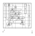
- FIG. 3 shows an illustrative space-designated grid 300 according to various embodiments.
- the space-designated grid 300 in this example can include left grid lines 302 and right grid lines 304 .
- Also illustrated in the space-designated grid 300 are a plurality of orthogonal circuit elements 306 , each classified with a first space-designated edge 308 A (e.g., left edge) and a second space designated edge 308 B (e.g., right edge), that dictate with which type of space-designated grid line (e.g., left grid line 302 or right grid line 304 ) that the orthogonal circuit element 306 will align.
- first space-designated edge 308 A e.g., left edge
- a second space designated edge 308 B e.g., right edge
- FIG. 4 shows a close-up depiction of a portion of the space-designated grid 300 , illustrating the pitch spacing O between two adjacent grid lines (e.g., left grid line 304 and right grid line 306 ).
- the spacing between adjacent grid lines is substantially uniform, at a distance O.
- the spacing between adjacent grid lines can be substantially non-uniform, and can be derived according to a grid spacing formula.
- FIG. 4 also illustrates the pitch distance (N) between neighboring lines within the same set of space designed lines (e.g., left grid lines 302 ; or right grid lines 304 ).
- FIG. 5 illustrates formation of example block masks 500 overlying spaces vacated by the plurality of orthogonal circuit elements 306 in the space-designated grid 300 in FIG. 3 .
- Aligning the plurality of orthogonal circuit elements 306 along grid lines e.g., left grid line 302 , right grid line 304 allows for efficient determination of the size, location and orientation of block masks 500 .
- the block masks 500 shown in the example of FIG. 5 can be efficiently manufacturable due to the alignment of orthogonal circuit elements 306 on the space-designated grid 300 .
- FIGS. 6-7 shows sample routing layouts 600 , 700 which illustrate how line-end stagger rules such as those shown and described herein allow for placement of lines with adequate spacings, tolerances, etc.
- the sample routing layouts 600 , 700 of FIGS. 6-7 illustrate first level vias 610 , second level vias 620 , first metal wire layers 630 , second metal wire layers 640 and second metal layer extensions 650 .
- aspects of the invention can be implemented as part of a business method that performs a process described herein on a subscription, advertising, and/or fee basis. That is, a service provider could offer to provide a orthogonal circuit element aware routing system as described herein.
- the service provider can manage (e.g., create, maintain, support, etc.) a computer system, such as computer system 102 ( FIG. 1 ), that performs a process described herein for one or more customers.
- the service provider can receive payment from the customer(s) under a subscription and/or fee agreement, receive payment from the sale of advertising to one or more third parties, and/or the like.
Abstract
Description
Claims (20)
Priority Applications (1)
| Application Number | Priority Date | Filing Date | Title |
|---|---|---|---|
| US13/908,562 US9245076B2 (en) | 2013-06-03 | 2013-06-03 | Orthogonal circuit element routing |
Applications Claiming Priority (1)
| Application Number | Priority Date | Filing Date | Title |
|---|---|---|---|
| US13/908,562 US9245076B2 (en) | 2013-06-03 | 2013-06-03 | Orthogonal circuit element routing |
Publications (2)
| Publication Number | Publication Date |
|---|---|
| US20140359548A1 US20140359548A1 (en) | 2014-12-04 |
| US9245076B2 true US9245076B2 (en) | 2016-01-26 |
Family
ID=51986672
Family Applications (1)
| Application Number | Title | Priority Date | Filing Date |
|---|---|---|---|
| US13/908,562 Expired - Fee Related US9245076B2 (en) | 2013-06-03 | 2013-06-03 | Orthogonal circuit element routing |
Country Status (1)
| Country | Link |
|---|---|
| US (1) | US9245076B2 (en) |
Cited By (4)
| Publication number | Priority date | Publication date | Assignee | Title |
|---|---|---|---|---|
| US10192021B1 (en) * | 2017-02-21 | 2019-01-29 | Cadence Design Systems, Inc. | Generating and inserting metal and metal etch shapes in a layout to correct design rule errors |
| US10580733B2 (en) | 2017-04-10 | 2020-03-03 | Samsung Electronics Co., Ltd. | Integrated circuit having heterogeneous source/drain and gate contacts |
| US10586009B2 (en) | 2017-12-12 | 2020-03-10 | International Business Machines Corporation | Hierarchical trim management for self-aligned double patterning |
| US10796064B2 (en) | 2018-08-14 | 2020-10-06 | International Business Machines Corporation | Autonomous placement to satisfy self-aligned double patterning constraints |
Families Citing this family (1)
| Publication number | Priority date | Publication date | Assignee | Title |
|---|---|---|---|---|
| US9767245B1 (en) | 2014-06-30 | 2017-09-19 | Cadence Design Systems, Inc. | Method, system, and computer program product for improving mask designs and manufacturability of electronic designs for multi-exposure lithography |
Citations (5)
| Publication number | Priority date | Publication date | Assignee | Title |
|---|---|---|---|---|
| US20110014786A1 (en) * | 2009-07-16 | 2011-01-20 | Cadence Design Systems, Inc. | Method, system, and program product for routing an integrated circuit to be manufactured by doubled patterning |
| US8214778B2 (en) * | 2007-08-02 | 2012-07-03 | Tela Innovations, Inc. | Methods for cell phasing and placement in dynamic array architecture and implementation of the same |
| US8356268B2 (en) * | 2007-08-02 | 2013-01-15 | Tela Innovations, Inc. | Integrated circuit device including dynamic array section with gate level having linear conductive features on at least three side-by-side lines and uniform line end spacings |
| US8741763B2 (en) * | 2012-05-07 | 2014-06-03 | Globalfoundries Inc. | Layout designs with via routing structures |
| US8813016B1 (en) * | 2013-01-28 | 2014-08-19 | Taiwan Semiconductor Manufacturing Company Limited | Multiple via connections using connectivity rings |
-
2013
- 2013-06-03 US US13/908,562 patent/US9245076B2/en not_active Expired - Fee Related
Patent Citations (6)
| Publication number | Priority date | Publication date | Assignee | Title |
|---|---|---|---|---|
| US8214778B2 (en) * | 2007-08-02 | 2012-07-03 | Tela Innovations, Inc. | Methods for cell phasing and placement in dynamic array architecture and implementation of the same |
| US8356268B2 (en) * | 2007-08-02 | 2013-01-15 | Tela Innovations, Inc. | Integrated circuit device including dynamic array section with gate level having linear conductive features on at least three side-by-side lines and uniform line end spacings |
| US20110014786A1 (en) * | 2009-07-16 | 2011-01-20 | Cadence Design Systems, Inc. | Method, system, and program product for routing an integrated circuit to be manufactured by doubled patterning |
| US8782586B2 (en) * | 2009-07-16 | 2014-07-15 | Cadence Design Systems, Inc. | Method, system, and program product for routing an integrated circuit to be manufactured by doubled patterning |
| US8741763B2 (en) * | 2012-05-07 | 2014-06-03 | Globalfoundries Inc. | Layout designs with via routing structures |
| US8813016B1 (en) * | 2013-01-28 | 2014-08-19 | Taiwan Semiconductor Manufacturing Company Limited | Multiple via connections using connectivity rings |
Non-Patent Citations (11)
Cited By (5)
| Publication number | Priority date | Publication date | Assignee | Title |
|---|---|---|---|---|
| US10192021B1 (en) * | 2017-02-21 | 2019-01-29 | Cadence Design Systems, Inc. | Generating and inserting metal and metal etch shapes in a layout to correct design rule errors |
| US10580733B2 (en) | 2017-04-10 | 2020-03-03 | Samsung Electronics Co., Ltd. | Integrated circuit having heterogeneous source/drain and gate contacts |
| US11437315B2 (en) | 2017-04-10 | 2022-09-06 | Samsung Electronics Co., Ltd. | Integrated circuit having heterogeneous gate contacts over active regions |
| US10586009B2 (en) | 2017-12-12 | 2020-03-10 | International Business Machines Corporation | Hierarchical trim management for self-aligned double patterning |
| US10796064B2 (en) | 2018-08-14 | 2020-10-06 | International Business Machines Corporation | Autonomous placement to satisfy self-aligned double patterning constraints |
Also Published As
| Publication number | Publication date |
|---|---|
| US20140359548A1 (en) | 2014-12-04 |
Similar Documents
| Publication | Publication Date | Title |
|---|---|---|
| US11935833B2 (en) | Method of forming power grid structures | |
| US10769342B2 (en) | Pin access hybrid cell height design | |
| KR101799644B1 (en) | Method and structure for mandrel and spacer patterning | |
| US9245076B2 (en) | Orthogonal circuit element routing | |
| US10817635B2 (en) | Multiple patterning method for semiconductor devices | |
| US8863048B1 (en) | Methods, systems, and articles of manufacture for implementing multiple-patterning-aware correct-by-construction layout processing for an electronic design | |
| US8850367B2 (en) | Method of decomposable checking approach for mask alignment in multiple patterning | |
| US11171089B2 (en) | Line space, routing and patterning methodology | |
| US11854966B2 (en) | Method of forming semiconductor device including deep vias | |
| US20190065653A1 (en) | Merged pillar structures and method of generating layout diagram of same | |
| US8296706B2 (en) | Handling two-dimensional constraints in integrated circuit layout | |
| Ou et al. | DSAR: DSA aware routing with simultaneous DSA guiding pattern and double patterning assignment | |
| CN104636530A (en) | Systems and methods for designing layouts for semiconductor device fabrication | |
| US10002222B2 (en) | System and method for perforating redundant metal in self-aligned multiple patterning | |
| US9286432B1 (en) | Methods, systems, and articles of manufacture for implementing correct-by-construction physical designs with multiple-patterning-awareness | |
| US10254642B2 (en) | Modifying design layer of integrated circuit (IC) using nested and non-nested fill objects | |
| TWI806874B (en) | Method and system for manufacturing integrated circuit by integration fill technique | |
| US20220043957A1 (en) | Method of forming merged pillar structures and method of generating layout diagram of same | |
| JP2009026045A (en) | Layout creating device and manufacturing method for semiconductor integrated circuit | |
| CN112117273A (en) | Integrated circuit device and method of forming the same | |
| Ban et al. | Self-aligned double-patterning layout decomposition for two-dimensional random metals for sub-10-nm node design | |
| US20230222278A1 (en) | Method for generating routing structure of semiconductor device | |
| US20230004702A1 (en) | Circuit arrangements having reduced dependency on layout environment | |
| Fang et al. | Simultaneous OPC-and CMP-aware routing based on accurate closed-form modeling | |
| Mirsaeedi | EDA Solutions for Double Patterning Lithography |
Legal Events
| Date | Code | Title | Description |
|---|---|---|---|
| AS | Assignment |
Owner name: INTERNATIONAL BUSINESS MACHINES CORPORATION, NEW Y Free format text: ASSIGNMENT OF ASSIGNORS INTEREST;ASSIGNORS:GEROUSIS, VASSILIOS;LIEBMANN, LARS W.;MANTIK, STEFANUS;AND OTHERS;SIGNING DATES FROM 20130510 TO 20130603;REEL/FRAME:030534/0977 |
|
| AS | Assignment |
Owner name: CADENCE DESIGN SYSTEMS, INC., CALIFORNIA Free format text: ASSIGNMENT OF ASSIGNORS INTEREST;ASSIGNOR:INTERNATIONAL BUSINESS MACHINES CORPORATION;REEL/FRAME:031607/0132 Effective date: 20131008 Owner name: INTERNATIONAL BUSINESS MACHINES CORPORATION, NEW Y Free format text: ASSIGNMENT OF ASSIGNORS INTEREST;ASSIGNOR:INTERNATIONAL BUSINESS MACHINES CORPORATION;REEL/FRAME:031607/0132 Effective date: 20131008 |
|
| STCF | Information on status: patent grant |
Free format text: PATENTED CASE |
|
| MAFP | Maintenance fee payment |
Free format text: PAYMENT OF MAINTENANCE FEE, 4TH YEAR, LARGE ENTITY (ORIGINAL EVENT CODE: M1551); ENTITY STATUS OF PATENT OWNER: LARGE ENTITY Year of fee payment: 4 |
|
| FEPP | Fee payment procedure |
Free format text: MAINTENANCE FEE REMINDER MAILED (ORIGINAL EVENT CODE: REM.); ENTITY STATUS OF PATENT OWNER: LARGE ENTITY |
|
| LAPS | Lapse for failure to pay maintenance fees |
Free format text: PATENT EXPIRED FOR FAILURE TO PAY MAINTENANCE FEES (ORIGINAL EVENT CODE: EXP.); ENTITY STATUS OF PATENT OWNER: LARGE ENTITY |
|
| STCH | Information on status: patent discontinuation |
Free format text: PATENT EXPIRED DUE TO NONPAYMENT OF MAINTENANCE FEES UNDER 37 CFR 1.362 |
|
| FP | Lapsed due to failure to pay maintenance fee |
Effective date: 20240126 |