US9240477B2 - Transistor-containing constructions and memory arrays - Google Patents
Transistor-containing constructions and memory arrays Download PDFInfo
- Publication number
- US9240477B2 US9240477B2 US14/189,808 US201414189808A US9240477B2 US 9240477 B2 US9240477 B2 US 9240477B2 US 201414189808 A US201414189808 A US 201414189808A US 9240477 B2 US9240477 B2 US 9240477B2
- Authority
- US
- United States
- Prior art keywords
- width
- construction
- gate
- along
- recess
- Prior art date
- Legal status (The legal status is an assumption and is not a legal conclusion. Google has not performed a legal analysis and makes no representation as to the accuracy of the status listed.)
- Active, expires
Links
Images


Classifications
-
- H01L29/7827—
-
- H—ELECTRICITY
- H10—SEMICONDUCTOR DEVICES; ELECTRIC SOLID-STATE DEVICES NOT OTHERWISE PROVIDED FOR
- H10D—INORGANIC ELECTRIC SEMICONDUCTOR DEVICES
- H10D64/00—Electrodes of devices having potential barriers
- H10D64/20—Electrodes characterised by their shapes, relative sizes or dispositions
- H10D64/27—Electrodes not carrying the current to be rectified, amplified, oscillated or switched, e.g. gates
- H10D64/311—Gate electrodes for field-effect devices
- H10D64/411—Gate electrodes for field-effect devices for FETs
- H10D64/511—Gate electrodes for field-effect devices for FETs for IGFETs
- H10D64/517—Gate electrodes for field-effect devices for FETs for IGFETs characterised by the conducting layers
- H10D64/518—Gate electrodes for field-effect devices for FETs for IGFETs characterised by the conducting layers characterised by their lengths or sectional shapes
-
- H01L27/10805—
-
- H01L29/4236—
-
- H—ELECTRICITY
- H10—SEMICONDUCTOR DEVICES; ELECTRIC SOLID-STATE DEVICES NOT OTHERWISE PROVIDED FOR
- H10B—ELECTRONIC MEMORY DEVICES
- H10B12/00—Dynamic random access memory [DRAM] devices
- H10B12/30—DRAM devices comprising one-transistor - one-capacitor [1T-1C] memory cells
-
- H—ELECTRICITY
- H10—SEMICONDUCTOR DEVICES; ELECTRIC SOLID-STATE DEVICES NOT OTHERWISE PROVIDED FOR
- H10B—ELECTRONIC MEMORY DEVICES
- H10B12/00—Dynamic random access memory [DRAM] devices
- H10B12/30—DRAM devices comprising one-transistor - one-capacitor [1T-1C] memory cells
- H10B12/34—DRAM devices comprising one-transistor - one-capacitor [1T-1C] memory cells the transistor being at least partially in a trench in the substrate
-
- H—ELECTRICITY
- H10—SEMICONDUCTOR DEVICES; ELECTRIC SOLID-STATE DEVICES NOT OTHERWISE PROVIDED FOR
- H10D—INORGANIC ELECTRIC SEMICONDUCTOR DEVICES
- H10D30/00—Field-effect transistors [FET]
- H10D30/60—Insulated-gate field-effect transistors [IGFET]
- H10D30/63—Vertical IGFETs
-
- H—ELECTRICITY
- H10—SEMICONDUCTOR DEVICES; ELECTRIC SOLID-STATE DEVICES NOT OTHERWISE PROVIDED FOR
- H10D—INORGANIC ELECTRIC SEMICONDUCTOR DEVICES
- H10D62/00—Semiconductor bodies, or regions thereof, of devices having potential barriers
- H10D62/10—Shapes, relative sizes or dispositions of the regions of the semiconductor bodies; Shapes of the semiconductor bodies
- H10D62/13—Semiconductor regions connected to electrodes carrying current to be rectified, amplified or switched, e.g. source or drain regions
- H10D62/149—Source or drain regions of field-effect devices
- H10D62/151—Source or drain regions of field-effect devices of IGFETs
-
- H10D64/01324—
-
- H—ELECTRICITY
- H10—SEMICONDUCTOR DEVICES; ELECTRIC SOLID-STATE DEVICES NOT OTHERWISE PROVIDED FOR
- H10D—INORGANIC ELECTRIC SEMICONDUCTOR DEVICES
- H10D64/00—Electrodes of devices having potential barriers
- H10D64/01—Manufacture or treatment
- H10D64/025—Manufacture or treatment forming recessed gates, e.g. by using local oxidation
- H10D64/027—Manufacture or treatment forming recessed gates, e.g. by using local oxidation by etching at gate locations
-
- H—ELECTRICITY
- H10—SEMICONDUCTOR DEVICES; ELECTRIC SOLID-STATE DEVICES NOT OTHERWISE PROVIDED FOR
- H10D—INORGANIC ELECTRIC SEMICONDUCTOR DEVICES
- H10D64/00—Electrodes of devices having potential barriers
- H10D64/20—Electrodes characterised by their shapes, relative sizes or dispositions
- H10D64/27—Electrodes not carrying the current to be rectified, amplified, oscillated or switched, e.g. gates
- H10D64/311—Gate electrodes for field-effect devices
- H10D64/411—Gate electrodes for field-effect devices for FETs
- H10D64/511—Gate electrodes for field-effect devices for FETs for IGFETs
- H10D64/512—Disposition of the gate electrodes, e.g. buried gates
- H10D64/513—Disposition of the gate electrodes, e.g. buried gates within recesses in the substrate, e.g. trench gates, groove gates or buried gates
Definitions
- Transistors are commonly utilized in integrated circuits, and may have many applications throughout memory, logic, etc. For instance, transistors may be utilized in dynamic random access memory (DRAM) arrays.
- DRAM dynamic random access memory
- a DRAM unit cell may comprise a transistor in combination with a capacitor.
- a continuing goal of integrated circuit fabrication is to create higher levels of integration, and accordingly to reduce size and spacing of existing components. It becomes increasingly more difficult to reduce the size of transistors due to short channel effects, higher contact resistance, and other complications.
- Transistor performance may be characterized by numerous metrics, including, for example, current flow through the on state (I on ) of the transistor, and current flow through the off state (I off ) of the transistor. It is desired to have high I on with low I off so that current is controlled and relatively unimpeded when the transistor is in the on state, and so that there is low current flow, if any, in the off state. However, there may be some level of leakage through transistors, especially as the transistors become increasingly smaller.
- An example leakage mechanism is drain-induced barrier lowering (DIBL), which can be particularly problematic in transistors having short channels.
- FIG. 1 is a three-dimensional view of an example embodiment transistor-containing construction.
- FIGS. 2-5 are cross-sectional side views of example embodiment transistor-containing constructions.
- FIG. 6 is a cross-sectional side view of example embodiment memory array.
- Some embodiments include new transistor configurations, logic, and/or memory arrays utilizing such configurations. Example embodiments are described below with reference to FIGS. 1-6 .
- a construction 10 comprises an example embodiment transistor 12 extending into a semiconductor material 14 .
- the material 14 may be any suitable semiconductor material; and in some embodiments may comprise, consist essentially of, or consist of monocrystalline silicon.
- the material 14 may be considered to comprise a semiconductor substrate.
- semiconductor substrate means any construction comprising semiconductive material, including, but not limited to, bulk semiconductive materials such as a semiconductive wafer (either alone or in assemblies comprising other materials), and semiconductive material layers (either alone or in assemblies comprising other materials).
- substrate refers to any supporting structure, including, but not limited to, the semiconductor substrates described above.
- material 14 may be part of a semiconductor substrate containing one or more other materials associated with integrated circuit fabrication. Some of the other materials may be under the shown region of construction 10 and/or may be laterally adjacent the shown region of construction 10 ; and may correspond to, for example, one or more of refractory metal materials, barrier materials, diffusion materials, insulator materials, etc.
- a recess 16 extends into the semiconductor material, and such recess is at least partially lined with gate dielectric material 18 .
- the gate dielectric material may comprise any suitable composition or combination of compositions; and in some embodiments may comprise, consist essentially of, or consist of silicon dioxide and/or high-k materials (with high-k meaning a dielectric constant greater than that of silicon dioxide).
- the recess 16 has a wide lower region 20 and a narrow upper region 22 .
- a width of the upper region may be less than or equal to about 75% of a width of the lower region, less than or equal to about 50% of the width of the lower region, etc.
- Gate material 24 is within a bottom portion of the wide lower region 20 , and insulative material 26 is over the gate material and directly contacts the gate material along an interface 27 .
- the insulative material is within a top portion of the wide lower region 20 , and is also within the narrow upper region 22 .
- material 26 may be omitted and gate material 24 may entirely fill both the lower region 20 and the upper region 22 .
- the gate dielectric material extends along both of the materials 24 and 26 in the shown embodiment, in other embodiments the material 18 may only be along gate material 24 and may be omitted from being along material 26 .
- the gate material 24 may comprise any suitable electrically conductive composition, or combination of compositions; and in some embodiments may comprise, consist essentially of, or consist of one or more of various metals (for example, tungsten, titanium, etc.), metal-containing compositions (for instance, metal nitride, metal carbide, metal silicide, etc.), and conductively-doped semiconductor materials (for instance, conductively-doped silicon, conductively-doped germanium, etc.).
- various metals for example, tungsten, titanium, etc.
- metal-containing compositions for instance, metal nitride, metal carbide, metal silicide, etc.
- conductively-doped semiconductor materials for instance, conductively-doped silicon, conductively-doped germanium, etc.
- the insulative material 26 may comprise any suitable composition or combination of compositions; and in some embodiments may comprise one or both of silicon dioxide and silicon nitride.
- a portion of the gate dielectric material 18 extends outwardly from a bottom of recess 16 and along the semiconductor material beneath the recess to form a “saddle region” 30 of the dielectric material. Additionally, a portion of the gate material 24 extends outwardly from the bottom of recess 16 and along the dielectric material 18 to form a “saddle region” 32 of the gate material. In the shown embodiment, the saddle region 32 of gate material 24 exactly overlaps the saddle region 30 of dielectric material 18 . In other embodiments, the dielectric material 18 may extend across a larger region than gate material 24 ; and accordingly saddle region 32 may be smaller than saddle region 30 .
- the saddle regions may be relatively symmetric relative to the gate material in the recess 16 (as shown), or may be asymmetric relative to such gate material. Also, the saddle regions may extend vertically, or may extend along off-vertical axes.
- Source/drain regions 34 and 36 extend within semiconductor material 14 , and along sides of recess 16 .
- the source/drain regions vertically overlap the interface 27 between insulative material 26 and gate material 24 .
- a channel region extends between source/drain region 34 and source/drain region 36 , and current across such channel region is gatedly controlled by electrical input to a transistor gate comprising material 24 .
- the source/drain regions 34 and 36 have steps 35 and 37 , respectively, where the wide region 20 of recess 16 transitions to the narrow region 22 .
- Conventional trenched transistors lack such steps and/or lack the saddle region 32 .
- the combination of the steps and saddle region may enable trenched structure 12 to be formed to have similar I off as conventional devices, while having substantially improved I on (for instance, I on may be improved by 20%, 30%, 50% or more).
- a narrow upper region 40 of the trenched structure 12 may enable wider upper contact surfaces 42 and 44 of source/drain regions 34 and 36 than would be available in comparable conventional devices.
- FIG. 2 shows a cross-sectional side view of the construction of FIG. 1 , and additionally shows isolation regions 50 and 52 along edges of the construction.
- the trenched structure 12 will be formed between a pair of isolation regions, as shown; and in other embodiments may be formed along only one isolation region (as discussed below with reference to FIG. 6 ), or may be formed in other configurations.
- the illustrated configuration having the trenched structure between a pair of isolation regions may be utilized in, for example, logic applications.
- the source/drain region 34 is shown to have an upper region with a relatively large width 51 , and a lower region with a relatively narrow width 53 .
- a ratio of width 53 to width 51 may be, for example, from about 0.1 to about 0.8; and in some embodiments may be from about 0.3 to about 0.5. In some example embodiments, width 53 may be less than or equal to about one-half of width 51 .
- the width 53 may be any suitable width, and in some embodiments may be less than or equal to about 5 nm.
- the width 51 may be any suitable width, and in some embodiments may be less than or equal to about 20 nm, less than or equal to about 10 nm, within a range of from about 3 nm to about 10 nm, within a range of from about 1 nm to about 10 nm, etc.
- Wide region 20 of recess 16 is shown having a width 56 .
- such width may be less than or equal to about 80 nanometers.
- the step 35 has a width 58 .
- the width 58 may be within a range of from about 3% of width 56 to about 15% of width 56 ; and in some embodiments may be within a range of from about 10% to about 95% of the width 51 .
- the trenched transistor structure 12 has an overall width 55 between isolation regions 50 and 52 along the cross-section of FIG. 2 .
- such overall width may be less or equal to about 120 nm.
- a plane 57 is shown extending vertically along a center of recess 16 (or, in other words, vertically along a center of materials 24 and 26 ).
- structure 12 substantially has mirror symmetry relative to such plane; and specifically, step 37 is about the same size as step 35 .
- the term “substantially” is utilized to indicate that structure 12 has mirror symmetry to within reasonable tolerances of fabrication and measurement.
- the illustrated trenched structure extends vertically (or at least substantially vertically), in other embodiments the trenched structure may extend along an off-vertical axis; and in such other embodiments the plane 57 that bisects the trenched structure may be along an off-vertical axis.
- a region of conductive material 24 within recess 16 may be part of a wordline that extends in and out of the page relative to the cross-section of FIG. 2 .
- Such wordline has a width 59 .
- the saddle region 32 has a width 61 , which may be less than or equal to the width 59 of the wordline. In some embodiments, the width 61 may be less than or equal to about 75% of the width 59 , less than or equal to about 50% of the width 59 , etc.
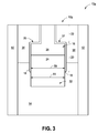
- FIG. 3 shows a construction 10 a comprising an example embodiment transistor 12 a in which width 61 of saddle region 32 is substantially the same as width 59 of the wordline within recess 16 .
- the narrow region 22 of recess 16 is inset relative to the wide region 20 by substantially equal steps 35 and 37 that are on opposing sides of the narrow region along the illustrated cross-section. Accordingly, there is substantial mirror symmetry relative to plane 57 .
- structures analogous to structure 12 may be asymmetric relative to plane 57 . Examples of such other embodiments are described with reference to FIGS. 4 and 5 .
- a construction 10 b comprises a recessed structure 12 b having only one step 35 .
- the step 37 ( FIG. 2 ) is missing, and instead a substantially vertical sidewall 70 extends along an entirety of one side of recess 16 (i.e., along both the narrow upper region 22 and wide lower region 20 of the recess).
- FIG. 5 shows a construction 10 c comprising a recessed structure 12 c having steps 35 and 37 which are of different widths relative to one another.
- FIGS. 4 and 5 may be advantageous in applications in which space limitations or fabrication limitations render it difficult to form a truly symmetric device; and/or may be advantageous in applications in which it is desired to fabricate a transistor device which is asymmetric relative to current flow relative to the paired source/drain regions.
- FIGS. 1-5 may be utilized in any of numerous applications, and may be, for example, utilized as field effect transistors in logic applications and/or memory applications.
- FIG. 6 shows an example embodiment memory array 100 in which recessed transistors of the type described above with reference to FIG. 2 are utilized in a DRAM application.
- a plurality of trenched transistors 100 - 103 are comprised by the array. Such transistors are identical to a structure described above with reference to FIG. 2 .
- the transistors may be examples of a large number of transistors formed along rows and columns of the array.
- the transistors comprise source/drain regions 110 - 114 ; with region 111 being shared between devices 101 and 102 .
- Isolation regions 104 and 105 extend into semiconductor material 14 , and separate some of the adjacent source/drain regions from one another.
- Memory structures 120 , 122 and 124 are electrically coupled to source/drain regions 110 , 112 and 113 , respectively; and bitlines 126 and 128 are electrically coupled to source/drain regions 111 and 114 , respectively.
- the gate material 24 within each of the transistors is coupled with a wordline 130 - 132 ; with the wordlines extending in and out of the page relative to the shown cross-sectional view.
- the memory structures 120 , 122 and 124 may comprise any suitable structures.
- the memory structures may comprise charge-storage devices such as, for example, capacitors.
- the combination of a capacitor with a transistor may form a memory unit, and each memory unit may be uniquely addressed through the combination of a wordline and a bitline.
- recesses 16 of FIGS. 1-6 may be fabricated utilizing multiple etches, in which one of the etches is isotropic and utilized to fabricate the lower wide portions of the recesses, and another etch is anisotropic and utilized to fabricate the narrow upper portions of the recesses.
- the electronic devices discussed above may be incorporated into electronic systems.
- Such electronic systems may be used in, for example, memory modules, device drivers, power modules, communication modems, processor modules, and application-specific modules, and may include multilayer, multichip modules.
- the electronic systems may be any of a broad range of systems, such as, for example, clocks, televisions, cell phones, personal computers, automobiles, industrial control systems, aircraft, etc.
- the various materials, substances, compositions, etc. described herein may be formed with any suitable methodologies, either now known or yet to be developed, including, for example, atomic layer deposition (ALD), chemical vapor deposition (CVD), physical vapor deposition (PVD), etc.
- ALD atomic layer deposition
- CVD chemical vapor deposition
- PVD physical vapor deposition
- dielectric and “electrically insulative” are both utilized to describe materials having insulative electrical properties. Both terms are considered synonymous in this disclosure.
- Some embodiments include a transistor-containing construction.
- the construction comprises a recess extending into a semiconductor material, with the recess having a narrow upper region and a wide lower region.
- Gate dielectric material is along the wide lower region of the recess.
- Gate material is within a bottom portion of the wide lower region.
- the gate dielectric material extends outwardly from a bottom of the recess and is along the semiconductor material beneath the recess.
- Gate material extends outwardly from the bottom of the recess and is along the gate dielectric material beneath the recess.
- Source/drain regions are within the semiconductor material along sides of the recess. The source/drain regions vertically overlap the interface of the insulative material and the gate material.
- Some embodiments include a transistor-containing construction.
- the construction comprises gate material within an opening in a semiconductor material, and spaced from the semiconductor material by gate dielectric material. Insulative material is over the gate material and directly contacts the gate material along an interface. The insulative material is within the opening. The insulative material has a narrow section over a wide section. The wide section has a same width as the gate material.
- a saddle region of the gate dielectric material extends outwardly from a bottom of the opening and is along the semiconductor material beneath the opening.
- a saddle region of the gate material extends outwardly from the bottom of the opening and is along the gate dielectric material beneath the opening.
- Source/drain regions are within the semiconductor material along sides of the electrically insulative material and gate material. The source/drain regions vertically overlap the interface of the insulative material and the gate material.
- Some embodiments include a memory array.
- the memory array includes a plurality of transistor constructions within a semiconductor material.
- Each transistor construction comprises gate material within an opening in the semiconductor material, and spaced from the semiconductor material by gate dielectric material.
- the gate material within the opening is part of a wordline.
- Each transistor construction comprises insulative material over the gate material and directly contacting the gate material along an interface.
- the insulative material is within the opening.
- the insulative material has a narrow section over a wide section. The wide section has a same width as the gate material.
- Each transistor construction comprises a saddle region of the gate dielectric material extending outwardly from a bottom of the opening and along the semiconductor material beneath the opening.
- Each transistor construction comprises a saddle region of the gate material extending outwardly from the bottom of the opening and along the gate dielectric material beneath the opening.
- Each transistor construction comprises source/drain regions within the semiconductor material along sides of the electrically insulative material and gate material. The source/drain regions vertically overlap the interface of the insulative material and the gate material.
- the memory array includes a pair of adjacent transistor constructions sharing a source/drain region. The shared source/drain region is connected to a bitline.
- the adjacent transistor constructions also comprise source/drain regions which are not shared, and which are connected to memory structures.
Landscapes
- Insulated Gate Type Field-Effect Transistor (AREA)
- Semiconductor Memories (AREA)
Abstract
Description
Claims (35)
Priority Applications (4)
| Application Number | Priority Date | Filing Date | Title |
|---|---|---|---|
| US14/189,808 US9240477B2 (en) | 2014-02-25 | 2014-02-25 | Transistor-containing constructions and memory arrays |
| PCT/US2014/066171 WO2015130352A1 (en) | 2014-02-25 | 2014-11-18 | Transistor-containing constructions and memory arrays |
| TW103142485A TW201533889A (en) | 2014-02-25 | 2014-12-05 | Structure and memory array containing transistors |
| US14/964,923 US20160093709A1 (en) | 2014-02-25 | 2015-12-10 | Transistor-Containing Constructions and Memory Arrays |
Applications Claiming Priority (1)
| Application Number | Priority Date | Filing Date | Title |
|---|---|---|---|
| US14/189,808 US9240477B2 (en) | 2014-02-25 | 2014-02-25 | Transistor-containing constructions and memory arrays |
Related Child Applications (1)
| Application Number | Title | Priority Date | Filing Date |
|---|---|---|---|
| US14/964,923 Continuation US20160093709A1 (en) | 2014-02-25 | 2015-12-10 | Transistor-Containing Constructions and Memory Arrays |
Publications (2)
| Publication Number | Publication Date |
|---|---|
| US20150243782A1 US20150243782A1 (en) | 2015-08-27 |
| US9240477B2 true US9240477B2 (en) | 2016-01-19 |
Family
ID=53883038
Family Applications (2)
| Application Number | Title | Priority Date | Filing Date |
|---|---|---|---|
| US14/189,808 Active 2034-07-20 US9240477B2 (en) | 2014-02-25 | 2014-02-25 | Transistor-containing constructions and memory arrays |
| US14/964,923 Abandoned US20160093709A1 (en) | 2014-02-25 | 2015-12-10 | Transistor-Containing Constructions and Memory Arrays |
Family Applications After (1)
| Application Number | Title | Priority Date | Filing Date |
|---|---|---|---|
| US14/964,923 Abandoned US20160093709A1 (en) | 2014-02-25 | 2015-12-10 | Transistor-Containing Constructions and Memory Arrays |
Country Status (3)
| Country | Link |
|---|---|
| US (2) | US9240477B2 (en) |
| TW (1) | TW201533889A (en) |
| WO (1) | WO2015130352A1 (en) |
Cited By (2)
| Publication number | Priority date | Publication date | Assignee | Title |
|---|---|---|---|---|
| US20160093709A1 (en) * | 2014-02-25 | 2016-03-31 | Micron Technology, Inc. | Transistor-Containing Constructions and Memory Arrays |
| US20220246757A1 (en) * | 2021-02-04 | 2022-08-04 | Nanya Technology Corporation | Semiconductor device and method for manufacturing the same |
Families Citing this family (1)
| Publication number | Priority date | Publication date | Assignee | Title |
|---|---|---|---|---|
| US11437481B2 (en) * | 2020-06-30 | 2022-09-06 | Nanya Technology Corporation | Semiconductor device with T-shaped buried gate electrode and method for forming the same |
Citations (2)
| Publication number | Priority date | Publication date | Assignee | Title |
|---|---|---|---|---|
| US5510630A (en) * | 1993-10-18 | 1996-04-23 | Westinghouse Electric Corporation | Non-volatile random access memory cell constructed of silicon carbide |
| US8859367B2 (en) * | 2010-07-09 | 2014-10-14 | Micron Technology, Inc. | Gate constructions of recessed access devices and methods of forming gate constructions of recessed access devices |
Family Cites Families (7)
| Publication number | Priority date | Publication date | Assignee | Title |
|---|---|---|---|---|
| US5362665A (en) * | 1994-02-14 | 1994-11-08 | Industrial Technology Research Institute | Method of making vertical DRAM cross point memory cell |
| US7560359B2 (en) * | 2004-11-26 | 2009-07-14 | Samsung Electronics Co., Ltd. | Methods of forming asymmetric recesses and gate structures that fill such recesses and related methods of forming semiconductor devices that include such recesses and gate structures |
| KR100720238B1 (en) * | 2006-01-23 | 2007-05-23 | 주식회사 하이닉스반도체 | Semiconductor element and manufacturing method thereof |
| KR100724575B1 (en) * | 2006-06-28 | 2007-06-04 | 삼성전자주식회사 | Semiconductor device having buried gate electrode and forming method thereof |
| KR20080090812A (en) * | 2007-04-06 | 2008-10-09 | 주식회사 하이닉스반도체 | Fin gate formation method of semiconductor device |
| KR20090098290A (en) * | 2008-03-13 | 2009-09-17 | 주식회사 하이닉스반도체 | Saddle Fin Transistor and Manufacturing Method Thereof |
| US9240477B2 (en) * | 2014-02-25 | 2016-01-19 | Micron Technology, Inc. | Transistor-containing constructions and memory arrays |
-
2014
- 2014-02-25 US US14/189,808 patent/US9240477B2/en active Active
- 2014-11-18 WO PCT/US2014/066171 patent/WO2015130352A1/en not_active Ceased
- 2014-12-05 TW TW103142485A patent/TW201533889A/en unknown
-
2015
- 2015-12-10 US US14/964,923 patent/US20160093709A1/en not_active Abandoned
Patent Citations (2)
| Publication number | Priority date | Publication date | Assignee | Title |
|---|---|---|---|---|
| US5510630A (en) * | 1993-10-18 | 1996-04-23 | Westinghouse Electric Corporation | Non-volatile random access memory cell constructed of silicon carbide |
| US8859367B2 (en) * | 2010-07-09 | 2014-10-14 | Micron Technology, Inc. | Gate constructions of recessed access devices and methods of forming gate constructions of recessed access devices |
Cited By (4)
| Publication number | Priority date | Publication date | Assignee | Title |
|---|---|---|---|---|
| US20160093709A1 (en) * | 2014-02-25 | 2016-03-31 | Micron Technology, Inc. | Transistor-Containing Constructions and Memory Arrays |
| US20220246757A1 (en) * | 2021-02-04 | 2022-08-04 | Nanya Technology Corporation | Semiconductor device and method for manufacturing the same |
| US11424360B1 (en) * | 2021-02-04 | 2022-08-23 | Nanya Technology Corporation | Semiconductor device and method for manufacturing the same |
| US11721759B2 (en) | 2021-02-04 | 2023-08-08 | Nanya Technology Corporation | Method for forming gate metal structure having portions with different heights |
Also Published As
| Publication number | Publication date |
|---|---|
| US20150243782A1 (en) | 2015-08-27 |
| TW201533889A (en) | 2015-09-01 |
| US20160093709A1 (en) | 2016-03-31 |
| WO2015130352A1 (en) | 2015-09-03 |
Similar Documents
| Publication | Publication Date | Title |
|---|---|---|
| US11062989B2 (en) | Assemblies which include wordlines over gate electrodes | |
| US10388864B2 (en) | Transistors and methods of forming transistors | |
| KR101840157B1 (en) | Field effect transistor constructions and memory arrays | |
| US8299562B2 (en) | Isolation structure and device structure including the same | |
| US9472542B2 (en) | DRAM arrays, semiconductor constructions and DRAM array layouts | |
| US7566620B2 (en) | DRAM including a vertical surround gate transistor | |
| US10347639B1 (en) | Integrated assemblies, and methods of forming integrated assemblies | |
| US10818667B2 (en) | Integrated assemblies which include carbon-doped oxide, and methods of forming integrated assemblies | |
| US10008503B1 (en) | Memory devices which include memory arrays | |
| US11450740B2 (en) | Integrated memory comprising gated regions between charge-storage devices and access devices | |
| KR20140029024A (en) | Junctionless semiconductor device having buried gate, module and system having the device and manufacturing method of the device | |
| US9240477B2 (en) | Transistor-containing constructions and memory arrays | |
| US20160056069A1 (en) | Methods of Forming Memory Arrays | |
| US20160126354A1 (en) | Methods of Forming Transistors | |
| US10622056B2 (en) | Apparatuses having compensator lines along wordlines and independently controlled relative to the wordlines | |
| US10644005B2 (en) | Transistors and memory arrays | |
| CN117915661A (en) | Semiconductor structure and method for manufacturing semiconductor structure | |
| TW201515221A (en) | Semiconductor device and method of manufacturing same | |
| US20120313157A1 (en) | Dram cell having buried bit line and manufacturing method thereof |
Legal Events
| Date | Code | Title | Description |
|---|---|---|---|
| AS | Assignment |
Owner name: MICRON TECHNOLOGY, INC., IDAHO Free format text: ASSIGNMENT OF ASSIGNORS INTEREST;ASSIGNORS:PANDEY, DEEPAK;LIU, HAITAO;SIGNING DATES FROM 20140213 TO 20140220;REEL/FRAME:032296/0585 |
|
| STCF | Information on status: patent grant |
Free format text: PATENTED CASE |
|
| AS | Assignment |
Owner name: U.S. BANK NATIONAL ASSOCIATION, AS COLLATERAL AGENT, CALIFORNIA Free format text: SECURITY INTEREST;ASSIGNOR:MICRON TECHNOLOGY, INC.;REEL/FRAME:038669/0001 Effective date: 20160426 Owner name: U.S. BANK NATIONAL ASSOCIATION, AS COLLATERAL AGEN Free format text: SECURITY INTEREST;ASSIGNOR:MICRON TECHNOLOGY, INC.;REEL/FRAME:038669/0001 Effective date: 20160426 |
|
| AS | Assignment |
Owner name: MORGAN STANLEY SENIOR FUNDING, INC., AS COLLATERAL AGENT, MARYLAND Free format text: PATENT SECURITY AGREEMENT;ASSIGNOR:MICRON TECHNOLOGY, INC.;REEL/FRAME:038954/0001 Effective date: 20160426 Owner name: MORGAN STANLEY SENIOR FUNDING, INC., AS COLLATERAL Free format text: PATENT SECURITY AGREEMENT;ASSIGNOR:MICRON TECHNOLOGY, INC.;REEL/FRAME:038954/0001 Effective date: 20160426 |
|
| AS | Assignment |
Owner name: U.S. BANK NATIONAL ASSOCIATION, AS COLLATERAL AGENT, CALIFORNIA Free format text: CORRECTIVE ASSIGNMENT TO CORRECT THE REPLACE ERRONEOUSLY FILED PATENT #7358718 WITH THE CORRECT PATENT #7358178 PREVIOUSLY RECORDED ON REEL 038669 FRAME 0001. ASSIGNOR(S) HEREBY CONFIRMS THE SECURITY INTEREST;ASSIGNOR:MICRON TECHNOLOGY, INC.;REEL/FRAME:043079/0001 Effective date: 20160426 Owner name: U.S. BANK NATIONAL ASSOCIATION, AS COLLATERAL AGEN Free format text: CORRECTIVE ASSIGNMENT TO CORRECT THE REPLACE ERRONEOUSLY FILED PATENT #7358718 WITH THE CORRECT PATENT #7358178 PREVIOUSLY RECORDED ON REEL 038669 FRAME 0001. ASSIGNOR(S) HEREBY CONFIRMS THE SECURITY INTEREST;ASSIGNOR:MICRON TECHNOLOGY, INC.;REEL/FRAME:043079/0001 Effective date: 20160426 |
|
| AS | Assignment |
Owner name: JPMORGAN CHASE BANK, N.A., AS COLLATERAL AGENT, ILLINOIS Free format text: SECURITY INTEREST;ASSIGNORS:MICRON TECHNOLOGY, INC.;MICRON SEMICONDUCTOR PRODUCTS, INC.;REEL/FRAME:047540/0001 Effective date: 20180703 Owner name: JPMORGAN CHASE BANK, N.A., AS COLLATERAL AGENT, IL Free format text: SECURITY INTEREST;ASSIGNORS:MICRON TECHNOLOGY, INC.;MICRON SEMICONDUCTOR PRODUCTS, INC.;REEL/FRAME:047540/0001 Effective date: 20180703 |
|
| AS | Assignment |
Owner name: MICRON TECHNOLOGY, INC., IDAHO Free format text: RELEASE BY SECURED PARTY;ASSIGNOR:U.S. BANK NATIONAL ASSOCIATION, AS COLLATERAL AGENT;REEL/FRAME:047243/0001 Effective date: 20180629 |
|
| MAFP | Maintenance fee payment |
Free format text: PAYMENT OF MAINTENANCE FEE, 4TH YEAR, LARGE ENTITY (ORIGINAL EVENT CODE: M1551); ENTITY STATUS OF PATENT OWNER: LARGE ENTITY Year of fee payment: 4 |
|
| AS | Assignment |
Owner name: MICRON TECHNOLOGY, INC., IDAHO Free format text: RELEASE BY SECURED PARTY;ASSIGNOR:MORGAN STANLEY SENIOR FUNDING, INC., AS COLLATERAL AGENT;REEL/FRAME:050937/0001 Effective date: 20190731 |
|
| AS | Assignment |
Owner name: MICRON SEMICONDUCTOR PRODUCTS, INC., IDAHO Free format text: RELEASE BY SECURED PARTY;ASSIGNOR:JPMORGAN CHASE BANK, N.A., AS COLLATERAL AGENT;REEL/FRAME:051028/0001 Effective date: 20190731 Owner name: MICRON TECHNOLOGY, INC., IDAHO Free format text: RELEASE BY SECURED PARTY;ASSIGNOR:JPMORGAN CHASE BANK, N.A., AS COLLATERAL AGENT;REEL/FRAME:051028/0001 Effective date: 20190731 |
|
| MAFP | Maintenance fee payment |
Free format text: PAYMENT OF MAINTENANCE FEE, 8TH YEAR, LARGE ENTITY (ORIGINAL EVENT CODE: M1552); ENTITY STATUS OF PATENT OWNER: LARGE ENTITY Year of fee payment: 8 |