US9231209B2 - Nanocomposite material, tunable resistor device, and method - Google Patents
Nanocomposite material, tunable resistor device, and method Download PDFInfo
- Publication number
- US9231209B2 US9231209B2 US14/081,409 US201314081409A US9231209B2 US 9231209 B2 US9231209 B2 US 9231209B2 US 201314081409 A US201314081409 A US 201314081409A US 9231209 B2 US9231209 B2 US 9231209B2
- Authority
- US
- United States
- Prior art keywords
- variable
- conductivity
- composite
- oxide
- composite material
- Prior art date
- Legal status (The legal status is an assumption and is not a legal conclusion. Google has not performed a legal analysis and makes no representation as to the accuracy of the status listed.)
- Expired - Fee Related, expires
Links
- 239000000463 material Substances 0.000 title claims abstract description 100
- 238000000034 method Methods 0.000 title claims description 24
- 239000002114 nanocomposite Substances 0.000 title abstract description 11
- 239000002131 composite material Substances 0.000 claims abstract description 108
- 239000004020 conductor Substances 0.000 claims abstract description 72
- 239000000203 mixture Substances 0.000 claims abstract description 25
- 239000011148 porous material Substances 0.000 claims description 42
- 239000002245 particle Substances 0.000 claims description 38
- GNRSAWUEBMWBQH-UHFFFAOYSA-N oxonickel Chemical compound [Ni]=O GNRSAWUEBMWBQH-UHFFFAOYSA-N 0.000 claims description 27
- 229910000480 nickel oxide Inorganic materials 0.000 claims description 26
- XUIMIQQOPSSXEZ-UHFFFAOYSA-N Silicon Chemical compound [Si] XUIMIQQOPSSXEZ-UHFFFAOYSA-N 0.000 claims description 22
- 229910052710 silicon Inorganic materials 0.000 claims description 22
- 239000010703 silicon Substances 0.000 claims description 22
- 150000004706 metal oxides Chemical class 0.000 claims description 17
- 229910044991 metal oxide Inorganic materials 0.000 claims description 16
- 239000010931 gold Substances 0.000 claims description 11
- PXHVJJICTQNCMI-UHFFFAOYSA-N Nickel Chemical compound [Ni] PXHVJJICTQNCMI-UHFFFAOYSA-N 0.000 claims description 10
- 229910052751 metal Inorganic materials 0.000 claims description 10
- 239000002184 metal Substances 0.000 claims description 10
- PCHJSUWPFVWCPO-UHFFFAOYSA-N gold Chemical compound [Au] PCHJSUWPFVWCPO-UHFFFAOYSA-N 0.000 claims description 9
- 229910052737 gold Inorganic materials 0.000 claims description 9
- 239000007787 solid Substances 0.000 claims description 9
- XLOMVQKBTHCTTD-UHFFFAOYSA-N Zinc monoxide Chemical compound [Zn]=O XLOMVQKBTHCTTD-UHFFFAOYSA-N 0.000 claims description 8
- 239000010416 ion conductor Substances 0.000 claims description 8
- VYPSYNLAJGMNEJ-UHFFFAOYSA-N Silicium dioxide Chemical compound O=[Si]=O VYPSYNLAJGMNEJ-UHFFFAOYSA-N 0.000 claims description 7
- 239000004065 semiconductor Substances 0.000 claims description 7
- BQCADISMDOOEFD-UHFFFAOYSA-N Silver Chemical compound [Ag] BQCADISMDOOEFD-UHFFFAOYSA-N 0.000 claims description 6
- GWEVSGVZZGPLCZ-UHFFFAOYSA-N Titan oxide Chemical compound O=[Ti]=O GWEVSGVZZGPLCZ-UHFFFAOYSA-N 0.000 claims description 6
- 229910052709 silver Inorganic materials 0.000 claims description 6
- 239000004332 silver Substances 0.000 claims description 6
- 229910052759 nickel Inorganic materials 0.000 claims description 5
- BASFCYQUMIYNBI-UHFFFAOYSA-N platinum Chemical compound [Pt] BASFCYQUMIYNBI-UHFFFAOYSA-N 0.000 claims description 5
- XHCLAFWTIXFWPH-UHFFFAOYSA-N [O-2].[O-2].[O-2].[O-2].[O-2].[V+5].[V+5] Chemical compound [O-2].[O-2].[O-2].[O-2].[O-2].[V+5].[V+5] XHCLAFWTIXFWPH-UHFFFAOYSA-N 0.000 claims description 4
- 238000000151 deposition Methods 0.000 claims description 4
- 230000008021 deposition Effects 0.000 claims description 4
- 229910052732 germanium Inorganic materials 0.000 claims description 4
- GNPVGFCGXDBREM-UHFFFAOYSA-N germanium atom Chemical compound [Ge] GNPVGFCGXDBREM-UHFFFAOYSA-N 0.000 claims description 4
- 238000000206 photolithography Methods 0.000 claims description 4
- 229910052814 silicon oxide Inorganic materials 0.000 claims description 4
- 229910001935 vanadium oxide Inorganic materials 0.000 claims description 4
- 239000011787 zinc oxide Substances 0.000 claims description 4
- JKFYKCYQEWQPTM-UHFFFAOYSA-N 2-azaniumyl-2-(4-fluorophenyl)acetate Chemical compound OC(=O)C(N)C1=CC=C(F)C=C1 JKFYKCYQEWQPTM-UHFFFAOYSA-N 0.000 claims description 3
- JBRZTFJDHDCESZ-UHFFFAOYSA-N AsGa Chemical compound [As]#[Ga] JBRZTFJDHDCESZ-UHFFFAOYSA-N 0.000 claims description 3
- 229910001218 Gallium arsenide Inorganic materials 0.000 claims description 3
- 229910021612 Silver iodide Inorganic materials 0.000 claims description 3
- GBRBMTNGQBKBQE-UHFFFAOYSA-L copper;diiodide Chemical compound I[Cu]I GBRBMTNGQBKBQE-UHFFFAOYSA-L 0.000 claims description 3
- 229910000449 hafnium oxide Inorganic materials 0.000 claims description 3
- WIHZLLGSGQNAGK-UHFFFAOYSA-N hafnium(4+);oxygen(2-) Chemical compound [O-2].[O-2].[Hf+4] WIHZLLGSGQNAGK-UHFFFAOYSA-N 0.000 claims description 3
- 229940096017 silver fluoride Drugs 0.000 claims description 3
- 229940045105 silver iodide Drugs 0.000 claims description 3
- REYHXKZHIMGNSE-UHFFFAOYSA-M silver monofluoride Chemical compound [F-].[Ag+] REYHXKZHIMGNSE-UHFFFAOYSA-M 0.000 claims description 3
- 238000002207 thermal evaporation Methods 0.000 claims description 3
- 239000004408 titanium dioxide Substances 0.000 claims description 3
- BYMUNNMMXKDFEZ-UHFFFAOYSA-K trifluorolanthanum Chemical compound F[La](F)F BYMUNNMMXKDFEZ-UHFFFAOYSA-K 0.000 claims description 3
- 229910052782 aluminium Inorganic materials 0.000 claims description 2
- XAGFODPZIPBFFR-UHFFFAOYSA-N aluminium Chemical compound [Al] XAGFODPZIPBFFR-UHFFFAOYSA-N 0.000 claims description 2
- -1 arsenide Substances 0.000 claims description 2
- 238000000313 electron-beam-induced deposition Methods 0.000 claims description 2
- 238000009830 intercalation Methods 0.000 claims description 2
- 229910052697 platinum Inorganic materials 0.000 claims description 2
- 230000004044 response Effects 0.000 claims description 2
- GYHNNYVSQQEPJS-UHFFFAOYSA-N Gallium Chemical compound [Ga] GYHNNYVSQQEPJS-UHFFFAOYSA-N 0.000 claims 1
- RNILVRNKISZRLD-UHFFFAOYSA-N [O-2].[O-2].[Ti+4].[O-2].[Hf+4] Chemical compound [O-2].[O-2].[Ti+4].[O-2].[Hf+4] RNILVRNKISZRLD-UHFFFAOYSA-N 0.000 claims 1
- 229910052733 gallium Inorganic materials 0.000 claims 1
- 239000000470 constituent Substances 0.000 abstract description 4
- 238000004891 communication Methods 0.000 abstract description 2
- 229910021426 porous silicon Inorganic materials 0.000 description 14
- 238000005259 measurement Methods 0.000 description 9
- 238000013528 artificial neural network Methods 0.000 description 8
- 238000002149 energy-dispersive X-ray emission spectroscopy Methods 0.000 description 7
- 230000002688 persistence Effects 0.000 description 7
- 230000006399 behavior Effects 0.000 description 6
- 239000000654 additive Substances 0.000 description 5
- 230000008859 change Effects 0.000 description 5
- 230000006870 function Effects 0.000 description 5
- 238000004519 manufacturing process Methods 0.000 description 5
- 238000012360 testing method Methods 0.000 description 5
- KRHYYFGTRYWZRS-UHFFFAOYSA-N Fluorane Chemical compound F KRHYYFGTRYWZRS-UHFFFAOYSA-N 0.000 description 4
- KBLQERBHKPBBRJ-UHFFFAOYSA-N [O].[Si].[Ni] Chemical compound [O].[Si].[Ni] KBLQERBHKPBBRJ-UHFFFAOYSA-N 0.000 description 4
- 238000003825 pressing Methods 0.000 description 4
- 239000000243 solution Substances 0.000 description 4
- 239000004593 Epoxy Substances 0.000 description 3
- 238000000137 annealing Methods 0.000 description 3
- 230000007547 defect Effects 0.000 description 3
- 238000013461 design Methods 0.000 description 3
- 238000009826 distribution Methods 0.000 description 3
- 238000009396 hybridization Methods 0.000 description 3
- 150000002500 ions Chemical class 0.000 description 3
- 229910052760 oxygen Inorganic materials 0.000 description 3
- 230000008569 process Effects 0.000 description 3
- 238000001878 scanning electron micrograph Methods 0.000 description 3
- LFQSCWFLJHTTHZ-UHFFFAOYSA-N Ethanol Chemical compound CCO LFQSCWFLJHTTHZ-UHFFFAOYSA-N 0.000 description 2
- 238000002441 X-ray diffraction Methods 0.000 description 2
- 230000000996 additive effect Effects 0.000 description 2
- 239000000853 adhesive Substances 0.000 description 2
- 230000001070 adhesive effect Effects 0.000 description 2
- QVGXLLKOCUKJST-UHFFFAOYSA-N atomic oxygen Chemical compound [O] QVGXLLKOCUKJST-UHFFFAOYSA-N 0.000 description 2
- 238000000498 ball milling Methods 0.000 description 2
- 230000008901 benefit Effects 0.000 description 2
- 238000012512 characterization method Methods 0.000 description 2
- 239000000945 filler Substances 0.000 description 2
- 238000011049 filling Methods 0.000 description 2
- 230000004907 flux Effects 0.000 description 2
- 238000013507 mapping Methods 0.000 description 2
- 239000011159 matrix material Substances 0.000 description 2
- 238000001883 metal evaporation Methods 0.000 description 2
- 150000002739 metals Chemical class 0.000 description 2
- 238000002156 mixing Methods 0.000 description 2
- 238000012986 modification Methods 0.000 description 2
- 230000004048 modification Effects 0.000 description 2
- 238000012544 monitoring process Methods 0.000 description 2
- QPJSUIGXIBEQAC-UHFFFAOYSA-N n-(2,4-dichloro-5-propan-2-yloxyphenyl)acetamide Chemical compound CC(C)OC1=CC(NC(C)=O)=C(Cl)C=C1Cl QPJSUIGXIBEQAC-UHFFFAOYSA-N 0.000 description 2
- 239000002105 nanoparticle Substances 0.000 description 2
- 210000002569 neuron Anatomy 0.000 description 2
- 239000001301 oxygen Substances 0.000 description 2
- 238000000926 separation method Methods 0.000 description 2
- 235000012239 silicon dioxide Nutrition 0.000 description 2
- 239000000377 silicon dioxide Substances 0.000 description 2
- 238000004528 spin coating Methods 0.000 description 2
- 239000000126 substance Substances 0.000 description 2
- 210000000225 synapse Anatomy 0.000 description 2
- 238000009827 uniform distribution Methods 0.000 description 2
- XNWFRZJHXBZDAG-UHFFFAOYSA-N 2-METHOXYETHANOL Chemical compound COCCO XNWFRZJHXBZDAG-UHFFFAOYSA-N 0.000 description 1
- FAPWRFPIFSIZLT-UHFFFAOYSA-M Sodium chloride Chemical compound [Na+].[Cl-] FAPWRFPIFSIZLT-UHFFFAOYSA-M 0.000 description 1
- 239000003570 air Substances 0.000 description 1
- 239000012080 ambient air Substances 0.000 description 1
- 230000004888 barrier function Effects 0.000 description 1
- 239000011230 binding agent Substances 0.000 description 1
- 230000015572 biosynthetic process Effects 0.000 description 1
- 210000004556 brain Anatomy 0.000 description 1
- 239000003990 capacitor Substances 0.000 description 1
- 238000006243 chemical reaction Methods 0.000 description 1
- 239000003795 chemical substances by application Substances 0.000 description 1
- 239000013068 control sample Substances 0.000 description 1
- 239000013078 crystal Substances 0.000 description 1
- 229910021419 crystalline silicon Inorganic materials 0.000 description 1
- 238000013500 data storage Methods 0.000 description 1
- 230000003247 decreasing effect Effects 0.000 description 1
- 230000007123 defense Effects 0.000 description 1
- 238000001514 detection method Methods 0.000 description 1
- 230000005684 electric field Effects 0.000 description 1
- 239000003792 electrolyte Substances 0.000 description 1
- 239000008151 electrolyte solution Substances 0.000 description 1
- 238000000724 energy-dispersive X-ray spectrum Methods 0.000 description 1
- 238000005516 engineering process Methods 0.000 description 1
- 238000005530 etching Methods 0.000 description 1
- 230000001747 exhibiting effect Effects 0.000 description 1
- 238000003384 imaging method Methods 0.000 description 1
- 230000008595 infiltration Effects 0.000 description 1
- 238000001764 infiltration Methods 0.000 description 1
- 230000010365 information processing Effects 0.000 description 1
- 238000011835 investigation Methods 0.000 description 1
- 230000014759 maintenance of location Effects 0.000 description 1
- 239000002923 metal particle Substances 0.000 description 1
- 238000004377 microelectronic Methods 0.000 description 1
- 230000005012 migration Effects 0.000 description 1
- 238000013508 migration Methods 0.000 description 1
- 229940078487 nickel acetate tetrahydrate Drugs 0.000 description 1
- OINIXPNQKAZCRL-UHFFFAOYSA-L nickel(2+);diacetate;tetrahydrate Chemical compound O.O.O.O.[Ni+2].CC([O-])=O.CC([O-])=O OINIXPNQKAZCRL-UHFFFAOYSA-L 0.000 description 1
- 230000037361 pathway Effects 0.000 description 1
- 230000035515 penetration Effects 0.000 description 1
- 239000000843 powder Substances 0.000 description 1
- 230000009467 reduction Effects 0.000 description 1
- 238000009418 renovation Methods 0.000 description 1
- 229920006395 saturated elastomer Polymers 0.000 description 1
- 238000004626 scanning electron microscopy Methods 0.000 description 1
- 238000005245 sintering Methods 0.000 description 1
- 239000011780 sodium chloride Substances 0.000 description 1
- 235000002639 sodium chloride Nutrition 0.000 description 1
- 238000001228 spectrum Methods 0.000 description 1
- 238000003860 storage Methods 0.000 description 1
- 239000000758 substrate Substances 0.000 description 1
- 230000036962 time dependent Effects 0.000 description 1
- 239000011800 void material Substances 0.000 description 1
- 235000012431 wafers Nutrition 0.000 description 1
Images


Classifications
-
- H—ELECTRICITY
- H10—SEMICONDUCTOR DEVICES; ELECTRIC SOLID-STATE DEVICES NOT OTHERWISE PROVIDED FOR
- H10N—ELECTRIC SOLID-STATE DEVICES NOT OTHERWISE PROVIDED FOR
- H10N70/00—Solid-state devices without a potential-jump barrier or surface barrier, and specially adapted for rectifying, amplifying, oscillating or switching
- H10N70/011—Manufacture or treatment of multistable switching devices
- H10N70/061—Patterning of the switching material
- H10N70/066—Patterning of the switching material by filling of openings, e.g. damascene method
-
- H—ELECTRICITY
- H10—SEMICONDUCTOR DEVICES; ELECTRIC SOLID-STATE DEVICES NOT OTHERWISE PROVIDED FOR
- H10N—ELECTRIC SOLID-STATE DEVICES NOT OTHERWISE PROVIDED FOR
- H10N70/00—Solid-state devices without a potential-jump barrier or surface barrier, and specially adapted for rectifying, amplifying, oscillating or switching
- H10N70/20—Multistable switching devices, e.g. memristors
- H10N70/24—Multistable switching devices, e.g. memristors based on migration or redistribution of ionic species, e.g. anions, vacancies
-
- H01L45/1683—
-
- H01L45/08—
-
- H01L45/1226—
-
- H01L45/1253—
-
- H01L45/1266—
-
- H01L45/14—
-
- H01L45/146—
-
- H01L45/1608—
-
- H—ELECTRICITY
- H10—SEMICONDUCTOR DEVICES; ELECTRIC SOLID-STATE DEVICES NOT OTHERWISE PROVIDED FOR
- H10N—ELECTRIC SOLID-STATE DEVICES NOT OTHERWISE PROVIDED FOR
- H10N70/00—Solid-state devices without a potential-jump barrier or surface barrier, and specially adapted for rectifying, amplifying, oscillating or switching
- H10N70/011—Manufacture or treatment of multistable switching devices
- H10N70/021—Formation of the switching material, e.g. layer deposition
-
- H—ELECTRICITY
- H10—SEMICONDUCTOR DEVICES; ELECTRIC SOLID-STATE DEVICES NOT OTHERWISE PROVIDED FOR
- H10N—ELECTRIC SOLID-STATE DEVICES NOT OTHERWISE PROVIDED FOR
- H10N70/00—Solid-state devices without a potential-jump barrier or surface barrier, and specially adapted for rectifying, amplifying, oscillating or switching
- H10N70/801—Constructional details of multistable switching devices
- H10N70/821—Device geometry
- H10N70/823—Device geometry adapted for essentially horizontal current flow, e.g. bridge type devices
-
- H—ELECTRICITY
- H10—SEMICONDUCTOR DEVICES; ELECTRIC SOLID-STATE DEVICES NOT OTHERWISE PROVIDED FOR
- H10N—ELECTRIC SOLID-STATE DEVICES NOT OTHERWISE PROVIDED FOR
- H10N70/00—Solid-state devices without a potential-jump barrier or surface barrier, and specially adapted for rectifying, amplifying, oscillating or switching
- H10N70/801—Constructional details of multistable switching devices
- H10N70/841—Electrodes
- H10N70/8416—Electrodes adapted for supplying ionic species
-
- H—ELECTRICITY
- H10—SEMICONDUCTOR DEVICES; ELECTRIC SOLID-STATE DEVICES NOT OTHERWISE PROVIDED FOR
- H10N—ELECTRIC SOLID-STATE DEVICES NOT OTHERWISE PROVIDED FOR
- H10N70/00—Solid-state devices without a potential-jump barrier or surface barrier, and specially adapted for rectifying, amplifying, oscillating or switching
- H10N70/801—Constructional details of multistable switching devices
- H10N70/881—Switching materials
- H10N70/883—Oxides or nitrides
- H10N70/8833—Binary metal oxides, e.g. TaOx
-
- Y—GENERAL TAGGING OF NEW TECHNOLOGICAL DEVELOPMENTS; GENERAL TAGGING OF CROSS-SECTIONAL TECHNOLOGIES SPANNING OVER SEVERAL SECTIONS OF THE IPC; TECHNICAL SUBJECTS COVERED BY FORMER USPC CROSS-REFERENCE ART COLLECTIONS [XRACs] AND DIGESTS
- Y10—TECHNICAL SUBJECTS COVERED BY FORMER USPC
- Y10S—TECHNICAL SUBJECTS COVERED BY FORMER USPC CROSS-REFERENCE ART COLLECTIONS [XRACs] AND DIGESTS
- Y10S977/00—Nanotechnology
- Y10S977/70—Nanostructure
- Y10S977/778—Nanostructure within specified host or matrix material, e.g. nanocomposite films
- Y10S977/779—Possessing nanosized particles, powders, flakes, or clusters other than simple atomic impurity doping
Definitions
- the present invention relates generally to composite materials, variable resistor devices, and the processes for making the composite materials and variable resistor devices.
- a type of variable resistor device commonly referred to as a “memristor” is a passive two-terminal circuit element in which its resistive state depends upon the voltage or current history of the element. More specifically, the resistive state is characterized by the relationship between the charge and flux. The resistance may vary continuously, or it may change discontinuously between distinct, non-volatile resistance states in resistively switched devices. Memristors retain their resistive states even when no potential is applied across them. They provide opportunity for improved solutions for high-density and energy efficient non-volatile data storage.
- Memristors can behave as a digital as well as analogdevice, and therefore, they are not only feasible for performing storage operations but they can also serve as components of analog computer architectures such as artificial neural networks (ANNs), which can out-perform von Neumann architectures in many computational tasks.
- ANNs artificial neural networks
- the use of memristors in ANNs is desirable because such components may facilitate the conversion of software-based ANN implementations to entirely hardware-based platforms which are faster, more efficient and easier to manufacture. Nevertheless, the use of memristors in many practical implementations is prohibited because macroscale and high-power memristor devices have not been achievable.
- Nanometer-scale memristive devices can be used in many integrated microelectronics applications, however, they have a low current density tolerance and thus their use in high-power system applications is limited.
- the most widely investigated and successfully demonstrated class of materials for memristive phenomena are metal-oxides.
- memristive metal-oxide devices ionic defects migrate under the influence of an applied electric field and vary in density throughout the volume of the metal oxide. Variable resistance arises when the defect mobility is high enough to cause defect density gradients across the metal-oxide structure within practical time parameters.
- memristive materials and devices for broader application.
- a nanometer-scale composite material colloquially referred to as a “nanocomposite” comprises, by volume, from about 1% to about 99% variable-conductivity material and from about 99% to about 1% conductive material.
- the variable-conductivity material and conductive material comprise nanometer-scale particles which have an average size that ranges from about one nanometer to about one micron along a maximum lineal dimension of the particle.
- the composite material exhibits memristive properties when a voltage differential is applied to the composite material.
- the materials of the composite compositions described above are present in a volume ratio of variable-conductivity material to conductive material that ranges from about 99%:1% to about 1%:99%.
- a variable resistor device in another embodiment, comprises a composite material and a first electrode terminal and a second electrode terminal in electrical communication with the composite material.
- the composite material comprises, by volume, from about 1% to about 99% variable-conductivity material and from about 99% to about 1% conductive material.
- a method for making the composite material comprises hybridizing a nanometer-scale conductive material with a nanometer-scale variable-conductivity material to form a composite material comprising, by volume, from about 1% to about 99% variable-conductivity material and from about 99% to about 1% conductive material.
- the above method further includes applying pressure to the mixture to form a composite.
- the method further comprises fabricating a nanometer-scale conductive material into a film structure having pores formed therein, and hybridizing the variable-conductive material into the pores of the film structure material comprising, by volume, from about 1% to about 99% variable-conductivity material and from about 99% to about 1% conductive material.
- variable resistor devices can be tuned for various electronic application requirements ranging from discrete states to variable properties in analog devices and over a wide range of power usage.
- FIG. 1 is a schematic top view illustration of a variable resistor device, according to an embodiment of the present invention
- FIG. 2 is a schematic cross-sectional illustration of the variable resistor device of FIG. 1 , according to an embodiment of the present invention
- FIGS. 3 a , 3 b , 3 c and 3 d are side schematic profile images of the composite materials showing straight parallel pores, parallel branched pores; crossing straight pores, and highly tortuous and interconnected pores, respectively, according to an embodiment of the present invention
- FIG. 4 is a schematic illustration of an alternative variable resistor device, according to another embodiment of the present invention.
- FIG. 5 is a top-view scanning electronic microscope (SEM) image of a cross-section of a nickel-oxide hybridized porous silicon (Si) film which shows pore infiltration, according to an embodiment of the present invention
- FIG. 6 is a side profile SEM image of the hybridized nickel-oxide silicon NiO/Si film of FIG. 1 , according to an embodiment of the present invention
- FIGS. 7 to 9 are images of an energy-dispersive x-ray spectroscopy EDX spatial mapping of the silicon, oxygen and nickel concentrations/distributions, respectively, within the film of FIGS. 5-6 , according to an embodiment of the present invention
- FIG. 10 is a spectrum of x-ray diffraction (XRD) of a hybridized film of nickel-oxide/silicon (NiO/Si) film of FIGS. 5-6 , according to an embodiment of the present invention
- FIGS. 11 a is a current-voltage plot of the measured hysteresis loops of three different nickel oxide silicon NiO/Si variable resistors, according to an embodiment of the present invention
- FIG. 11 b is the logarithmic representation of the plots of FIG. 11 a , according to an embodiment of the present invention.
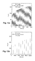
- FIGS. 12 a and 12 b illustrate current-voltage measurements of a nickel-oxide silicon variable resistor device when sinusoidal voltages are applied with a DC offset, according to an embodiment of the present invention.
- FIG. 13 a - 13 b illustrate state persistence measurements when a nickel-oxide silicon variable resistor device is exposed to an all-positive square-wave at different frequency, according to an embodiment of the present invention.
- a nanometer-scale composite material comprises, by volume, from about 1% to about 99% variable-conductivity material and from about 99% to about 1% conductive material, in another embodiment from about 10% to about 90% variable-conductivity material and from about 90% to about 10% conductive material, in another embodiment from about 25% to about 75% variable-conductivity material and from about 75% to about 25% conductive material, in another embodiment, from about 35% to about 65% variable-conductivity material and from about 65% to about 35% conductive material; and in yet another embodiment from about 45% to about 65% variable-conductivity material and from about 65% to about 45% conductive material.
- the variable-conductivity material and conductive material comprise nanometer-scale particles.
- nanometer-scale means that the particles have an average size that ranges from about one nanometer to about one micron along a lineal dimension of the particle, in alternative applications or embodiments from about one nanometer to about one thousand nanometers, and in yet other embodiments, from about one nanometer to about one hundred nanometers.
- the lineal dimension of a particle depends at least in part upon the geometry of the particle. For example, the average particle size is based on the diameter if the particle is spherical, or as another example, the average shape can be based on a lineal side of the particle.
- variable-conductivity material of the composite is a material that exhibits a variable conductivity under applied voltage, for example a metal oxide and a solid ionic conductor material.
- a solid ionic conductor material is a material that exhibits ionic conductivity including high-mobility ionic conductivity with some degree of electronic conduction.
- variable-conductivity materials that are metal oxides include, but are not limited to, nickel oxide, zinc oxide, titanium dioxide, hafnium oxide, silicon dioxide, vanadium oxide and combinations thereof.
- variable-conductivity materials that are solid ionic conductor materials include, but are not limited to, silver iodide, copper iodide, lanthanum fluoride, silver fluoride, and combinations thereof.
- the conductive material of the composite is a metal or a semi-conductive material that is doped.
- conductive or semi-conductive metals include but are not limited to, silver, gold, silicon, germanium, gallium arsenide and combinations thereof.
- the semi-conductive metal may be a doped material, for example p-type or n-type doped material.
- the composites herein can optionally include additive materials in an amount, by volume, that is less than about 25%, in another embodiment from about 0.01% to about 10%, and in another embodiment from about 0.01% to about 5%.
- Additive materials include, but are not limited to, fillers, adhesives or binders, chemical solutions, and in another embodiment less than about 1%.
- additives can function as fillers to fill void regions between small particles.
- Additives that function as adhesives including but not limited to epoxy, for example a conductive epoxy such as a silver-based epoxy, can be used to promote adhesion and mechanical stability of the nanocomposite in its final solid form.
- the variable conductivity material can be present in a chemical solution, for example a nickel-oxide solution gel or “sol gel”.
- variable-conductivity material relative to the conductive material affects the electrical properties of the composite.
- variable-conductivity material and the conductive material of the composites described above are present in a volume ratio of variable-conductivity material to conductive material, i.e. volume variable-conductivity material: volume conductive material that ranges from about 1%:99% to 99%:1%; in another embodiment from about 10%:90% to about 90%:10%; in another embodiment from about 35%:65% to about 75%:25%; in another embodiment from about 40%:60% to about 70%:30%; and in another embodiment from about 48%:52% to about 60%:40%.
- An example of a metal-oxide/conductive material nanocomposite is a nickel oxide/silicon composite which comprises, by volume, from about 1% to about 99% nickel oxide and from about 99% to about 1% silicon; in another embodiment from about 10% to about 90% nickel oxide and from about 90% to about 10% silicon; in another embodiment from about 25% to about 75% nickel oxide and from about 75% to about 25% silicon; and in yet another embodiment, from about 35% to about 65% nickel oxide and from about 65% to about 35% silicon.
- the volume ratio of nickel-oxide to silicon ranges from about 1%:99% to about 99%:1%; in another embodiment from about 10%:90% to about 90%:10%; in another embodiment from about 35%:65% to about 75%:25%; and in another embodiment from about 48%:52% to about 60%:40%.
- the composite materials, or “nanocomposites” described herein, having varying compositions of a variable-conductivity material and a conductive material exhibit memristive properties or “memristance” when a voltage differential is applied to the composite materials.
- the change in volume ratio results in variation in electrical properties, including the conductivity and resistivity of the composites.
- the material interfaces between the variable-conductivity material and the conductive material i.e. trans-interface conduction, impacts the overall conductivity of the composite material.
- memristance may be defined as the electrical behavior of a passive, two-terminal device which is indicative of a memristor or memristive system and cannot be associated with the other three fundamental linear two-terminal devices, i.e., resistors, capacitors or inductors. Particular behaviors are described, in general, by a fundamental mathematical relationship between device charge and flux, and therefore, these devices are categorized as memristive devices or in some cases, memristive systems.
- memristive device and “memristor” can be used interchangeably.
- Composite materials that exhibit memristive properties, or memristance as used herein means that the when a voltage differential is applied to the composite the device exhibits: 1) “variable conductivity” and 2) “state persistence. More specifically, the term “variable conductivity” means that the conductivity of the device varies as a function of the applied voltage history. As a voltage is applied across the device over time, the current through the device will increase (or decrease, in certain cases) in a particular manner, for example as described by a mathematical definition. In the case of an ideal memristor the current may increase indefinitely while, in practical devices, it will increase until some saturation is encountered. However, when the voltage is removed, current will cease to flow. This behavior results in a “pinched” hysteresis current-voltage curve when a sinusoidally varying voltage is applied.
- State persistence is closely related to the term “non-volatility” which is more commonly applied to binary-state memory elements; however, as used herein, state-persistence also applies to continuous- or analog-state memristors. State-persistence implies that, if the conductivity is allowed to grow to some value and the applied voltage is removed, i.e. made zero, that the conductivity will retain that value for some time termed the “state-persistence time” and may be measured at a later point in time by application of a subsequent voltage and simultaneous current measurement.
- the ranges of conductivity variation and the minimum conductivity of the various embodiments of nanocornposites herein are considered for potential applications of memristors.
- the minimum conductivity also known as the maximum resistance state
- the minimum conductivity is typically the resistance state observed when the device has been exposed to zero net applied voltage, and it may be considered the device “off” state in many applications.
- Nanocomposites may facilitate the design of devices with different minimum conductivity as well as different ranges of conductivity variation.
- a nanocomposite which is comprised of 10% nickel oxide and 90% gold exhibits a high minimum conductivity due to the highly conductive gold component, while also exhibiting a very narrow range of conductivity variation due to the small volume of NiO.
- a device composed of 90% nickel oxide and 10% gold exhibit a much lower minimum conductivity due to the highly resistive NiO and a greater range of conductivity variation.
- a minimum range of conductivity variation for a memristor should be at least about 50% of the minimum conductivity to allow for detection or measurement of state changes.
- the variation in conductivity of the devices for practical application typically ranges from about 50% to about 100,000% of the minimum device conductivity. For some applications, a much greater relative conductivity variation is desired than in others.
- one of the devices presented in FIG. 11 b (the 30 mA/cm 2 curve) comprising a nanocomposite of nickel oxide and silicon shows a conductivity change of approximately two orders of magnitude ( ⁇ 10,000%) under the specific conditions applied. These conductivity ranges can be converted into resistance ranges to exemplify practical values.
- a memristive device with a maximum resistance (“off” state) of about 1.5 k ⁇ would have a practical minimum resistance of as high as about 1 k ⁇ which would be reached after some period of applied voltage.
- a device with a maximum resistance of about 1 M ⁇ is likely to have a minimum resistance of as low as about 1 k ⁇ , or smaller.
- devices with a maximum resistance of about 7.5 M ⁇ , to be practical must have a minimum resistance no greater than 5 G ⁇ .
- Characterization of electrical properties such as the variable conductivity and state-persistence of composite materials described herein, may be demonstrated with two straight-forward electrical testing protocol.
- To demonstrate variation in conductivity it is common to apply a sinusoidally varying voltage with zero DC offset, such that the voltage across the device oscillates between positive and negative values.
- the current-voltage curve for a memristive device will exhibit a hysteresis loop which spans the first and third quadrants of a Cartesian plot and will cross the origin. This hysteresis curve is therefore described as “pinched” and is a generally accepted trait of memristors and memristive systems.
- Testing for state-persistence involves the application of voltage pulses which are positive and are separated by periods of zero voltage (i.e., a pulse train). When tested in this manner, memristors exhibit the growth of current (i.e., decrease in resistance) with each successive pulse, until saturation is reached, and zero current during periods of zero applied voltage. This continued current growth is attributed to the property of state-persistence.
- the maximum amount of zero-voltage time (lowest pulse repetition rate) over which memristive devices will exhibit state-persistence is referred to as the maximum state-persistence time.
- variable resistor device or memristor can have a bearing on the properties of the ultimate products obtained. For example, size impacts the response speed of the variable-conductivity element, and resistance changes more quickly for smaller particle size than for larger particle size. This is due, at least in part, to smaller total distance that ions must travel across a particle/grain, as well as increased ion mobility (or conductivity).
- Each composite material may have its own optimum particle size depending upon the material constituents.
- Many variable-conductivity materials e.g. metal oxides, solid ionic conductor materials, etc.
- conductive materials e.g.
- doped silicon are available commercially in nanometer particle size ranges, however, they may be commercially available in larger particle size ranges, in which case such source particles can be mechanically worked, such as by ball milling or mechanical mixing, to reduce the particle size to the desired range. Mechanical working breaks up any agglomerates of metal particles which may have formed and, additionally, insures homogenous distribution of the individual particles.
- variable resistor device 10 comprising a first electrode terminal, a second electrode terminal, and a composite material of variable-conductive material and conductive material including the embodiments of the composite materials described above.
- FIG. 1 and FIG. 2 are illustrations of the top view and side view, respectively, of a representative two-terminal variable-resistor device 10 , or memristor, according to an embodiment of the present invention.
- Variable resistor device 10 includes a composite material 20 comprising a variable-conductivity material and a conductive material, as described above, and contact electrodes 22 and 24 .
- the contacts 22 , 24 are shown in an interdigitated design 26 , however, a variety of alternative designs are possible.
- the electrical contacts can be fabricated via conventional photolithography, along with thermal metal evaporation, in order to produce contacts with separations ranging from about 1 to about 100 ⁇ m and in another embodiment from about 2 to about 25 ⁇ m.
- a variety of metals can be used to fabricate the contacts including, but not limited to, nickel (Ni), aluminum (Al), platinum (Pt), and gold (Au) to ensure electrical connections are made to the devices.
- Ni nickel
- Al aluminum
- Pt platinum
- Au gold
- the memristive behavior of the variable-conductivity device is expected to be dictated predominately by the hybrid material composition, not the contact metal, although the contact metal may contribute an additional Shottky-like energy barrier.
- the various embodiments of composite material 20 comprise nanometer-scale particles of a variable-conductivity material, for example a solid ionic conductor material, or a metal oxide, and a conductive material, such as a metal or a semiconductor. These materials are combined in controlled compositions and ratios so as to alter or tune the electronic properties of the device. The composition and volumetric ratio of the two materials dictates the fraction of the composite which exhibits variable conductivity, thereby determining the dynamic conductivity properties.
- a variable-conductivity material for example a solid ionic conductor material, or a metal oxide
- a conductive material such as a metal or a semiconductor.
- FIG. 2 is a side view illustration of the memristor 10 of FIG. 1 .
- This illustration shows composite material 20 fabricated as a film structure of conductive material 28 having pores formed therein and variable-conductivity 30 within the pores.
- the composite material 20 is a matrix of conductive material, or host material, and the variable-conductivity material, or intercalating material, that fills the pores of the conductive material to make up the film structure.
- the porosity of the host material can vary widely depending on the average size of the pores. In one embodiment the average size of the pore, measured in diameter or length for example, can range from about one nanometer to about 100 microns, in another embodiment from about one nanometer to about one micron, and in another embodiment from about one nanometer to about 100 nanometers.
- the nanocrystallite size of the variable-conductivity material is dictated at least in part by the pore size it fills, and the physical and electrical characteristics of the composite, such as for example resistivity, can be varied depending upon the average pore size
- the geometry of the pore can be one of several three-dimensional geometric shapes, including but not limited to, a cylinder, a rectangular channel, and any polygonal channel for example.
- a broad diversity of pore morphologies can be readily achieved in conductive material, or host matrix, through appropriate selection of doping type, crystal orientation, and electrolyte composition.
- Porous silicon morphologies can be qualitatively characterized as follows: 1) parallel pores; 2) parallel branched pores; 3) crossing, straight pores; and 4) tortuous, interconnected pores as shown in FIGS. 3 a , 3 b , 3 e , and 3 d , respectively.
- the thickness of composite material 20 can range from about 100 nm to about 100 ⁇ m, and in another embodiment from about 200 nm to about 10 ⁇ m.
- the composite material 20 can also have discrete portions of varying porosity, materials, and morphology in a single composite material, such as a film, and also in a completed variable resistor device 10 .
- FIG. 4 illustrates a variable resistor device 50 in accordance with another embodiment of the present invention.
- Variable resistor device 50 includes an insulating container 52 filled with a nanoparticle composite material 54 which comprises a variable-conductivity material and a conductive material and integrated metal electrodes 60 , 62 to facilitate electrical contact.
- the variable resistor device includes a composite material of any of the embodiments described above, an insulating container and two electrodes.
- the composite material 54 is in the form of a “particle re-composite” and is useful in large or macroscale devices.
- the nanocrystallite size of the variable-conductivity material is dictated by the pore size in which it is formed.
- the nanocrystallite size is determined by the powder production process, for example sintering and ball-milling processes.
- Such macro-scale devices for example the canister-type variable resistor, may be engineered in size and geometry (e.g. length and diameter) to increase power dissipation for systems where higher power tolerance is needed.
- Composite materials which are particle re-composites provide a highly economical means of producing large-scale memristive devices. As described in the examples below, combining porous silicon (Si) particles with ball-milled particulates of metal-oxide material yields a composite structure that allows for controlled volumetric ratio of the silicon and metal-oxide constituents and enables variation of grain-boundary density through particle size.
- composition ranges possible in a nanocomposite can depend on the form or physical structure of the composite.
- a porous semiconductor material or host that is infiltrated with variable-conductivity, material such as metal-oxide may require a minimum amount of the semiconductor, i.e. 10% by volume to allow physical formation of the composite.
- a particle re-composite is only limited by measurement and combination technique and may comprise substantially less of one component.
- a film of porous metal or semiconductor infiltrated with variable-conductivity material can have a ratio of conductive material to variable-conductivity material that ranges from about 10%: 90% to about 90% : 10%.
- the ratio of conductive material to variable-conductivity material can range from about 1%: 99% to about 99% : 1%.
- variable resistor devices 10 , 50 depends at least in part upon the voltage or the current history of the material when applied to the material via two terminals.
- the resistance may vary continuously or it may change discontinuously between distinct resistance states.
- the minimum instantaneous resistance or “chord resistance” can be altered to an extent of three orders of magnitude by varying the composition and ratios of the variable-conductivity material and conductive material constituents of the composites.
- the examples below show that variable resistance devices having nickel-oxide/silicon composites that had 48%, 55% and 60% nickel-oxide, by volume, exhibited resistances that ranged from 165 k ⁇ to 964 M ⁇ . This large capacity to tune memristive behavior is useful in the fabrication of large-scale memristive elements.
- ANNs Artificial neural networks
- ANNs are a variety of computation architectures which rely upon highly parallel information processing as a means of executing certain types of algorithms in an efficient manner.
- ANNs are modeled loosely after the structure of the human brain, which is composed of a large number of neurons, each connected to a number of other neurons by pathways called synapses.
- Memristors which are variable resistance devices, may be used as elements which function as synapses. While many ANNs are software-based implementations of this architecture, a memristor-based ANN would be entirely hardware-based, and is therefore expected to be more efficient and easier to produce/manufacture.
- a method for making the composite material comprises hybridizing a nanometer-scale conductive material with a nanometer-scale variable-conductivity material to form a composite material in accordance with the present invention, including the compositions described herein.
- Hybridizing can be accomplished by various methods.
- the above method can include combining the conductive material and variable-conductivity material by mixing the materials and by further applying pressure to the mixture (e.g. pressing or compacting) to form a composite.
- the method for making a composite comprises fabricating a nanometer-scale conductive material into a film structure having pores formed therein, and hybridizing the variable-conductive material into the pores of the film structure material comprising variable-conductivity material and conductive material.
- Hybridizing a conductive material film structure can be achieved in a variety of processes.
- the method further comprises forming pores within the film structure and filling the pores of the film structure with particles of the variable-conductive material via at least one of the following techniques: sol-gel deposition through spin coating, thermal deposition, and electron beam deposition.
- Another optional step is annealing at a temperature depending upon the composition of the composite formed, for example, a NiO/Si composite can be annealed at a temperature that ranges from about 400° C. to about 800° C.
- the method comprises forming pores within the film structure, breaking the film structure into particles of conductive material, combining variable-conductivity material particles with the conductive material particles to produce a mixture, and applying pressure to the mixture to form a composite material that is a particle re-composite.
- the electrical contacts can be formed on the composite materials via photolithography and thermal metal evaporation methods in order to produce a two-terminal variable resistor device.
- Variable resistor devices were made by nickel-oxide NiO hybridization with porous silicon Si through sol-gel deposition. The devices were characterized by current-voltage testing under a time varying applied voltage, as described in the examples below.
- PSi Two-terminal variable resistor devices were fabricated from NiO-hybridized PSi films.
- PSi was formed using an anodic electrochemical etching procedure employing a hydrofluoric acid (HF) electrolyte solution (15% HF, 15% H 2 O, 70% EtOH, by volume) to produce films of ⁇ 1 ⁇ m thickness from n + -doped Si wafers ( ⁇ 100>, 0.01 ⁇ cm).
- Samples of three different average pore sizes were etched by applying currents of 25, 30 and 35 mA ⁇ cm ⁇ 2 . Average pore diameters of the films were measured to be approximately 19 nm, 27 nm, and 41 nm by scanning electron microscopy (SEM).
- NiO hybridization was carried out by sol-gel spin coating and subsequent high-temperature annealing.
- the sol-gel was composed of nickel acetate tetrahydrate in 2-methoxyethanol (0.05 g ⁇ mL ⁇ 1 ) and was drop cast onto samples and allowed to saturate the surface for several minutes before being spun at 2,500 RPM to ensure uniformity. Films were then annealed at 700° C. for 2 hours in an air ambient to promote crystallinity of the NiO.
- FIG. 5 A top-view SEM image of a hybrid NiO/Si film is shown in FIG. 5 .
- the image indicates that the majority of the pores are filled (lighter color interiors).
- FIG. 6 shows a side-profile SEM image of a high porosity hybrid NiO/Si composite film alongside energy dispersive x-ray spectroscopy (EDX) spatial maps.
- EDX was carried out with a Zeiss Merlin VP SEM/STEM instrument and all elements were quantified by monitoring and spatial mapping of the respective k ⁇ emission wavelength. Additional SEM was performed using a Raith eLiNE electron microscope. The pores were not maximally filled in this example.
- FIGS. 7-9 show the uniform distribution of elements Si, O, and Ni, respectively, within the film.
- X-ray diffraction spectra of the NiO-hybridized porous Si films reveal the expected diffraction peaks associated with the rocksalt (B 1 ) cubic structure NiO after annealing.
- EDX Energy dispersive x-ray spectroscopy
- NiO/PSi hybrid memristive devices were fabricated by conventional photolithography and thermal deposition of 100 nm-thick Au contacts (Angstrom Engineering deposition system). Circular contact patterns with an electrode separation of 20 ⁇ m were fabricated and the devices were thermally annealed for 3 minutes in ambient air to promote contact adhesion. Memristors were characterized electrically by monitoring the time varying current, I, with a Keithley 2400 source-meter. Hysteresis behavior was interrogated by supplying a 0.25 Hz sinusoidal source voltage, V s , amplitude ⁇ 10 V.
- FIGS. 11 a and 11 b show the hysteresis loops observed in the current-voltage curves of the varying porosity memristive devices (48%, 55% and 60%).
- the characteristic open, “pinched” current-voltage hysteresis exhibited by the devices indicates that they function as memristors.
- a trend in the hysteresis loops with increasing Si film porosity is evident. As film porosity was increased through increased etch current, the minimum instantaneous resistance, or chord resistance of the NiO/Si memristor increased.
- the smallest pore diameter films (19 nm) exhibited a minimum instantaneous resistance of 165 k ⁇ while the largest pore diameter NiO/P Si films (41 nm) exhibited a minimum instantaneous resistance of 962 M ⁇ .
- analogous devices composed of pure NiO on planar, non-porous silicon were also fabricated as a control sample.
- the pure NiO devices were highly resistive (>5 G ⁇ ) and exhibited no observable hysteresis loop over the voltage range examined.
- the dynamic range of the resistances exhibited by the devices also differs between composite films with different pore sizes, with the mid-range pore diameter (27 nm) film changing by more than two orders of magnitude.
- the relative range of variation in the resistances exhibited by the devices also differed between porosities.
- State-persistence measurements were made by supplying a 6 V amplitude sine wave voltage (12 V, peak-to-peak) with a DC offset of 6 V.
- variable magnitude (1-20 V) square-wave pulses with 1 s duration were applied with varying periods of zero applied voltage, ranging from 1-10000 s, while measuring current.
- Device measurements were corroborated using a custom made op-amp based current-source circuit.
- FIGS. 12 a and 12 b show current-voltage measurements of a NiO/Si variable resistor device having a 27 nanometer pore diameter when a sinusoidal voltage is applied with a DC offset and when 20 Volt, 1 second pulses were applied, respectively. Results showed an increasing current (decreasing resistance) trend for a NiO/PSi device under a DC-biased sinusoidal applied voltage indicating resistance state persistence.
- a sinusoidal voltage was applied with a DC offset equal to the AC wave amplitude, such that the voltage was instantaneously zero at cycle minimums, shown in FIG. 12 a .
- the continued decrease in resistance of the device over multiple cycles was evident, showing state-persistence between cycles. It is noted that, after four cycles, the conductivity of the device saturated, indicating the minimum device resistance for the given applied voltage.
- Persistence times ranged from 10 s of seconds to more than 1000 s, likely due to differences in crystallite irregularity and pore filling uniformity between samples.
- FIG. 13 a - 13 b illustrate state persistence measurements when one such device was exposed to an all-positive square-wave with 0.2 Hz and 0.001 Hz period, respectively.
Abstract
Description
| TABLE 1 | ||||||
| Nickel- | ||||||
| Oxide | ||||||
| Vol. | Meas- | Chord | ||||
| Comp. | Vol. | Film | ured | Resis- | ||
| Ex- | (Film | Ratio | Pore | Voltage | Measured | tance |
| ample | Porosity) | NiO:Si | Size | (volts) | Current | (ohms) |
| Control | n/a | 100:0 | n/a | 0-10 |
2 × 10⁻⁹ | >5 | |
| 1 | |||||||
| Ex. 1 | 60% | 60:40 | 41 nm | 0-10 V | 1.04 × 10⁻⁸ | 962 | MΩ |
| Ex. 2 | 55% | 55:45 | 27 nm | 0-10 V | 5.3 × 10⁻⁶ | 1.89 | MΩ |
| Ex. 3 | 48% | 48:52 | 19 nm | 0-10 |
6 × 10⁻⁵ | 165 | kΩ |
Claims (32)
Priority Applications (1)
| Application Number | Priority Date | Filing Date | Title |
|---|---|---|---|
| US14/081,409 US9231209B2 (en) | 2012-11-16 | 2013-11-15 | Nanocomposite material, tunable resistor device, and method |
Applications Claiming Priority (2)
| Application Number | Priority Date | Filing Date | Title |
|---|---|---|---|
| US201261727263P | 2012-11-16 | 2012-11-16 | |
| US14/081,409 US9231209B2 (en) | 2012-11-16 | 2013-11-15 | Nanocomposite material, tunable resistor device, and method |
Publications (2)
| Publication Number | Publication Date |
|---|---|
| US20140138601A1 US20140138601A1 (en) | 2014-05-22 |
| US9231209B2 true US9231209B2 (en) | 2016-01-05 |
Family
ID=50727065
Family Applications (1)
| Application Number | Title | Priority Date | Filing Date |
|---|---|---|---|
| US14/081,409 Expired - Fee Related US9231209B2 (en) | 2012-11-16 | 2013-11-15 | Nanocomposite material, tunable resistor device, and method |
Country Status (1)
| Country | Link |
|---|---|
| US (1) | US9231209B2 (en) |
Cited By (7)
| Publication number | Priority date | Publication date | Assignee | Title |
|---|---|---|---|---|
| US9991328B2 (en) | 2016-08-25 | 2018-06-05 | International Business Machines Corporation | Tunable on-chip nanosheet resistor |
| US20180157783A1 (en) * | 2016-12-05 | 2018-06-07 | Synopsys, Inc. | Nano-wire resistance model |
| US10275706B2 (en) * | 2013-01-29 | 2019-04-30 | Hewlett Packard Enterprise Development Lp | Neuristor-based reservoir computing devices |
| US10685163B2 (en) | 2017-03-01 | 2020-06-16 | Synopsys, Inc. | Computationally efficient nano-scale conductor resistance model |
| US10714242B2 (en) | 2017-12-20 | 2020-07-14 | International Business Machines Corporation | Symmetrically tunable electrical resistor |
| US10740672B2 (en) * | 2018-03-30 | 2020-08-11 | Univerity Of Massachusetts | Capacitative artificial neural networks |
| US11915926B2 (en) | 2021-09-27 | 2024-02-27 | International Business Machines Corporation | Percolation doping of inorganic-organic frameworks for multiple device applications |
Families Citing this family (3)
| Publication number | Priority date | Publication date | Assignee | Title |
|---|---|---|---|---|
| WO2016153461A1 (en) * | 2015-03-20 | 2016-09-29 | Hewlett Packard Enterprise Development Lp | Memristive device with doped sol-gel switching layer |
| CN104966778B (en) * | 2015-05-07 | 2018-01-23 | 清华大学 | A kind of frequency response learner of long-term memory and preparation method thereof |
| WO2018004648A1 (en) * | 2016-07-01 | 2018-01-04 | Intel Corporation | Apparatuses, systems, and methods associated with a magnetoelectric cell including a magnetoelectric nanocomposite |
Citations (8)
| Publication number | Priority date | Publication date | Assignee | Title |
|---|---|---|---|---|
| US20090184397A1 (en) | 2008-01-22 | 2009-07-23 | Nadine Gergel-Hackett | Nonvolatile memory device and processing method |
| US7898844B2 (en) | 2008-10-31 | 2011-03-01 | Seagate Technology, Llc | Magnetic tunnel junction and memristor apparatus |
| US20110176353A1 (en) | 2008-12-23 | 2011-07-21 | Zhiyong Li | Memristive Device Having a Porous Dopant Diffusion Element |
| US20110309321A1 (en) * | 2010-06-21 | 2011-12-22 | Jianhua Yang | Memristors with a switching layer comprising a composite of multiple phases |
| US20120074378A1 (en) * | 2010-09-23 | 2012-03-29 | Wei Wu | Memory element having elastically deformable active region |
| US20120091421A1 (en) * | 2009-07-02 | 2012-04-19 | Dianzhong Wen | Nanostructure quick-switch memristor and method of manufacturing the same |
| US20140311790A1 (en) * | 2011-10-21 | 2014-10-23 | Jianhua Yang | Memristive element based on hetero-junction oxide |
| US9035272B2 (en) * | 2013-01-16 | 2015-05-19 | Hewlett-Packard Development Company, L.P. | Nanoparticle-based memristor structure |
-
2013
- 2013-11-15 US US14/081,409 patent/US9231209B2/en not_active Expired - Fee Related
Patent Citations (8)
| Publication number | Priority date | Publication date | Assignee | Title |
|---|---|---|---|---|
| US20090184397A1 (en) | 2008-01-22 | 2009-07-23 | Nadine Gergel-Hackett | Nonvolatile memory device and processing method |
| US7898844B2 (en) | 2008-10-31 | 2011-03-01 | Seagate Technology, Llc | Magnetic tunnel junction and memristor apparatus |
| US20110176353A1 (en) | 2008-12-23 | 2011-07-21 | Zhiyong Li | Memristive Device Having a Porous Dopant Diffusion Element |
| US20120091421A1 (en) * | 2009-07-02 | 2012-04-19 | Dianzhong Wen | Nanostructure quick-switch memristor and method of manufacturing the same |
| US20110309321A1 (en) * | 2010-06-21 | 2011-12-22 | Jianhua Yang | Memristors with a switching layer comprising a composite of multiple phases |
| US20120074378A1 (en) * | 2010-09-23 | 2012-03-29 | Wei Wu | Memory element having elastically deformable active region |
| US20140311790A1 (en) * | 2011-10-21 | 2014-10-23 | Jianhua Yang | Memristive element based on hetero-junction oxide |
| US9035272B2 (en) * | 2013-01-16 | 2015-05-19 | Hewlett-Packard Development Company, L.P. | Nanoparticle-based memristor structure |
Non-Patent Citations (127)
| Title |
|---|
| A. Fujimori and F. Minami, "Valence-Band Photoemission and Optical Absorption in Nickel Compounds," Phys. Rev. B, vol. 30, p. 957, 1984. |
| A.M. Ferrari, C. Pisani, F. Cinquini, L. Giordano, and G. Pacchioni, "Cationic and Anionic Vacancies on the Nio(100) Surface: DFT+U and Hybrid Functional Density Functional Theory Calculations," J. Chem., Phys., vol. 127, pp. 174711-174718, 2007. |
| B.A. Everitt, D. Wang, and J. M. Daughton, "Spin Valves with NiO Pinning Layer," 1996, pp. 4657-4659. |
| C. Kang, C. Phare, S.M. Weiss, Y.A. Vlasov, and S. Assefa, "Photonic Crystal Defects with Increased Surface Area for Improved Refractive Index Sensing," Conference on Lasers and Electro-Optics/International Quantum Electronics Conference, p. CTuL1, 2010. |
| C. Kang, C. Phare, Y.A. Vlasov, S. Assefa, and S. M. Weiss, "Photonic Crystal Slab Sensor with Enhanced Surface Area," Opt. Express, vol. 18, pp. 27930-27937, 2010. |
| C. Kang, C. Phare, Y.A. Vlasov, S. Assefa, and S.M. Weiss, "Optimization of Defect Hole Placement in Resonant Cavity Sensors," CLEO: 2011-Laser Applications to Photonics Applications, 2011. |
| C. Walczyk, C. Wenger, R. Sohal, M. Lukosius, A. Fox, J. Dabrowski, D. Wolansky, B. Tillack, H.-J. Mussig, and T. Schroeder, "Pulse-Induced Low-Power Resistive Switching in HfO2 Metal-Insulator-Metal Diodes for Nonvolatile Memory Applications," J. Appl. Phys., vol. 105, p. 114103, 2009. |
| C.E. Rossi, and W. Paul, "The Preparation of NiO Thin Films and their Use in Optical Measurements in the Visible and Ultraviolet," J. Phys. Chem. Solids, vol. 30, pp. 2295-2305, 1969. |
| C.-W. Nan and D.R. Clarke, "Effect of Variations in Grain Size and Grain Boundary Barrier Heights on the Current-Voltage Characteristics of ZnO Varistors," J. Am. Ceram. Soc., vol. 79, pp. 3185-3192, 1996. |
| D. Biolek, Z. Biolek, and V. Biolkova, "Pinched Hysteretic Loops of Ideal Memristors, Memcapacitors and Meminductors must be 'self-crossing'," Electron. Lett, vol. 47, 2011. |
| D. Stroud, "Generalized, Effective, Medium Approach to the Conductivity of an Inhomogeneous Material," Phys. Rev. B, vol. 12, pp. 3368-3373, 1975. |
| D.B. Strukov and R.S. Williams, "Exponential Ionic Drift: Fast Switching and Low Volatility of Thin-Film Memristors," Appl. Phys. A, vol. 94, pp. 515-519, 2009. |
| D.B. Strukov, G.S. Snider, D.R. Stewart, and R.S. Williams, "The Missing Memristor Found," Nature, vol. 453, pp. 80-83, 2008. |
| D.C. Kim, et al., "Electrical Observations of Filamentary Conductions for the Resistive Memory Switching in NiO Films," Applied Physics Letters, vol. 88, pp. 202102-202103, 2006. |
| D.C. Kim, S. Seo, S.E. Ahn, D.S. Suh, M.J. Lee, B.H. Park, I.K. Yoo, I.G. Baek, H.J. Kim, E.K. Yim,. J.E. Lee, S. O. Park, S. Kim, U.I. Chung, J.T. Moon, and B.I. Ryu, "Electrical Observations of Filamentary Conductions for the Resistive Memory Switching in NiO Films," Appl. Phys. Lett., vol. 88, pp. 202102-202103, 2006. |
| D.C. Look, "Recent Advances in ZnO Materials and Devices," Mater, Sci. Eng., B, vol. 80, pp. 383-387, 2001. |
| D.C. Look, D.C. Reynolds, J.R. Sizelove, R.L. Jones, C.W. Litton, G. Cantwell, and W.C. Harsch, "Electrical Properties of Bulk ZnO," Solid State Commun., vol. 105, pp. 399-401, 1998. |
| D.R. Clarke, "Varistor Ceramics," J. Am. Ceram. Soc., vol. 82, pp. 485-502, 1999. |
| D.-W. Kim, B.H. Park, R. Jung, and S.Seo, "Reversible Resistance Switching Behaviors of Pt/NiO/Pt Structures," Jpn. J. Appl. Phys., vol. 46, p. 5205, 2007. |
| D.-W. Kim, et al., "Reversible Resistance Switching Behaviors of Pt/NiO/Pt Structures," Japanese Journal of Applied Physics, vol. 46, p. 5205, 2007. |
| G. Chern, S.D. Berry, D.M. Lind, H. Mathias, and L.R. Testardi, "Modulated Electric-Conductivity in Fe3O4/NiO Superiattices," Appl. Phyl. Lett., vol. 58, pp. 2512-2513, Jun. 1991. |
| G. Rong and S.M. Weiss, "Biomolecule Size-Dependent Sensitivity of Porous Silicon Sensors," Phys. Status Solidi A, vol. 206, pp. 1365-1368, 2009. |
| G. Rong and S.M. Weiss, "Influence of Biomolecule Size on Performance of Nanostructured Sensing Devices," Proc. of SPIE, vol. 6769, p. 676909, 2007. |
| G. Rong, A. Najmaie, J.E. Sipe, and S.M. Wiess, "Nanoscale Porous Silicon Waveguide for Label-Free DNA Sensing," Biosensors & Bioelectronics, vol. 23, pp. 1572-1576, 2008. |
| G. Rong, J.D. Ryckman, R.L. Mernaugh and S.M. Weiss, "Label-Free Porous Silicon Membrane Waveguide for DNA Sensing," Appl. Phys. Left., vol. 93, p. 161109, 2008. |
| G. Wakefield, P.J. Dobson, Y.Y. Foo, A. Loni, A. Simons and J.L. Hutchison, "The Fabrication and Characterization of Nickel Oxide Films and Their Application as Contacts to Polymer/Porous Silicon Electroluminescent Devices," Semicond. Sci. Technol., vol. 12, pp. 1304-1309, 1997. |
| G.J.M. Janssen and W.C. Nieuwpoort, "Band Gap in NiO: A Cluster Study," Phys. Rev. B, vol. 38, p. 3449, 1988. |
| H. Kamal, E.K. Elmaghraby, S.A. Ali, and K. Abdel-Hady, "Characterization of Nickel Oxide Films Deposited at Different Substrate Temperatures Using Spray Pyrolysis," J. Cryst. Growth, vol. 262, pp. 424-434, 2004. |
| H. Ohta, M. Hirano, K. Nakahara, H. Maruta, T. Tanabe, M. Kamiya, T. Kamiya, and H. Hosono, "Fabrication and Photoresponse of a pn-heterojunction Diode Composed of Transparent Oxide Semiconductors, p-NiO and n-ZnO," Appl. Phys. Lett., vol. 83, pp. 1029-1031, 2003. |
| H. Ouyang, M. Christophersen and P.M. Fauchet, "Enhanced Control of Porous Silicon Morphology from Macropore to Mesopore Formation," Phys. Status Solidi A, vol. 202, pp. 1396-1401, 2005. |
| H. Wu, and L.-S. Wang, "A Study of Nickel Monoxide (NiO), Nickel Dioxide (ONiO), and Ni(O2) Complex by Anion Photoelectron Spectroscopy," J. Chem. Phys., vol. 107, pp. 16-21, 1997. |
| H. Wu, and L.-S. Wang, "Electronic Structure of Titanium Oxide Clusters: TiOy (y=1−3) and (TiO2)n (n=1−4)," J. Chem. Phys., vol. 107, 1997. |
| H. Wu, and L.-S. Wang, "Electronic Structure of Titanium Oxide Clusters: TiOy (y=1-3) and (TiO2)n (n=1-4)," J. Chem. Phys., vol. 107, 1997. |
| H.L. Tuller, "Ionic Conduction in Nanocrystalline Materials" Solid State Ionics, 2000, 131,143-157. |
| H.L. Tuller, "ionic Conduction in Nanocrystalline Materials," Solid State Ionics, vol. 131, pp. 143-157, 2000. |
| J. F. Gibbons and W.E. Beadle, "Switching Properties of Thin NiO Films," Solid-State Electronics, vol. 7, pp. 785-790, 1964. |
| J. Maier, "Ionic Conduction Space Charge Regions" Prog. Solid State Chem., 1995, 23, 171-263. |
| J. Maier, "On the Conductivity of Polycrystalline Materials," Berichte der Bunsengesellschaft für physikalische Chemie, vol. 90, pp. 26-33, 1986. |
| J. Maier, "Transport in Electroceramics: Micro-and-Nano-Structural Aspects" J. Eur. Ceram. Soc., 2004, 24, 1251-1257. |
| J. Wu and R.L. McCreery, "Solid State Electrochemistry is Molecular Heterojunctions as the Basis of the TiO2 "Memristor"," J. Electrochem. Soc., vol. 156, pp. P29-P37, Jan. 1, 2009. |
| J. Yang, J. Strachan, F. Miao, M.-X. Zhang, M. Pickett, W. Yi, D. Ohlberg, G. Medeiros-Ribeiro, and R. Williams, "Metal/TiO2 Interfaces for Memristive Switches," Appl. Phys. A, vol. 102, pp. 785-789, 2011. |
| J. Yang, M. Pickett, X. Li, D. Ohlberg, D. Stewart, and R. Williams, "Memristive Switching Mechanism for Metal/Oxide/Metal Nanodevices," Nat Nanotechnol, vol. 3, pp. 429-433, 2008. |
| J. Zaanen, G.A. Sawatzky, and J.W. Allen, "Band Gaps and Electronic Structure of Transition-Metal Compounds," Phys. Rev. Lett., vol. 55, p. 418, 1985. |
| J.C. Bruyer and B.K. Chakrabverty, "Switching and Negative Resistance in Thin Films of Nickel Oxide," Appl. Phys. Lett., vol. 16, pp. 40-43, 1969. |
| J.C. Scott, and L.D. Bozano "Nonvolatile Memory Elements Based on Organic Materials," Adv. Mater, vol. 19, pp. 1452-1463, 2007. |
| J.F. Gibbons and W. E. Beadle, "Switching Properties of Thin NiO Films," Solid-State Elect., vol. 7, p. 785, 1964. |
| J.-H. Choi, S. Nath, and J.-M. Myoung, "Controllable Resistance Switching Behavior of NiO/SiO2 Double Layers for Nonvolatile Memory Applications," Appl. Phys. Lett., vol. 95, p. 062105, 2009. |
| J.H. Kim, X. Li, L.-S. Wang, H.L. De Clercq, C.A. Fancher, O.C. Thomas, and K.H. Bowen, "Vibrationally Resovled Photoelectron Spectroscopy of MgO- and ZnO- and the Low-Lying Electronic States of MgO, MgO-, and ZnO," J. Phys. Chem. A, vol. 105, pp. 5709-5718, 2001. |
| J.-H. Park, L. Gu, G. Von Maltzahn, E. Ruoslahti, S.N. Bhatia and M.J. Sailor, "Biodegradable Luminescent Porous Silicon Nanoparticles for In Vivo Applications," Nat. Mater., vol. 8, pp. 331-336, 2009. |
| J.L. Lawrie and S.M. Weiss, "Silicon Photonics for Biosensing Applications," Silicon Photonics for Telecommunications and Biomedical Applications, S. Fathpour and B. Jalali, Eds., ed Boca Raton, Fl.: Taylor & Francis, 2011, pp. 201-230. |
| J.-M. Choi and S. Im, "Ultraviolet Enhanced Si-Photodetector Using p-NiO Films," Appl. Surf. Sci., vol. 244, pp. 435-438, 2005. |
| J.W. Mares, R.C. Boutwell, A. Scheurer, M. Falanga, and W.V. Schoenfeld, "Cubic ZnxMg1-xO and NixMg1-xO Thin Films Grown by Molecular Beam Epitaxy for Deep-UV Optoelectronic Applications," in SPIE, San Francisco, 2010, p. 76031B. |
| J.W. Mares, R.C. Boutwell, M. Wei, A. Scheurer, and W.V. Schoenfeld, "Deep-Ultraviolet Photodetectors from Epitaxially Grown NixMg1-xO," Appl. Phys. Left., vol. 97, p. 161113, 2010. |
| J.-W. Park, J.-W. Park, D.-Y. Kim and J.-K. Lee, "Reproducible Resistive Switching in Nanstoichiometric Nickel Oxide Films Grown by rf Reactive Sputtering for Resistive Random Access Memory Applications," J.Vac. Sci. Technol., A., vol. 23, pp. 1309-1313, 2005. |
| J-B. Yum, S. Kim, S. Seo, M.-J. Lee, D.C. Kim, S.E. Ahn, Y.S. Park, J. Kim, and H. Shin, "Random and Localized Resistive Switching Observation in Pt/NiO/Pt," Physica Status Solidi (RRL)-Rapid Research Letters, vol. 1, pp. 280-282, 2007. |
| K. Kobayashi, M. Yamaguchi, Y. Tomita, and Y. Maeda, "Fabrication and Characterization of In-Ga-Zn-O/NiO Structures," Thin Solid Films, vol. 516, pp. 5903-5906, 2008. |
| K. Oka, T. Yanagida, K. Nagashima, H. Tanaka, and T. Kawai, "Growth Atmosphere Dependence of Transport Properties of NiO Epitaxial Thin Films," J. Appl. Phys., vol. 104, pp. 013711-013714, 2008. |
| K. Tsunoda, K. Kinoshita, H. Noshiro, Y.Yamazaki, T. Iizuka, Y. Ito, A. Takashahi, A. Okano, Y. Sato, T. Fukano, M. Aoki, and Y. Sugiyama, "Low Power and High Speed Switching of Ti-Doped NiO ReRAM Under Unipolar Voltage Source of Less than 3 V," IEEE International Electron Devices Meeting, 2007, pp. 767-770. |
| K.C. Min, M. Kim, Y.H. You, S. S. Lee, Y.K. Lee, T. M. Chung, C.G. Kim, J. H. Hwang, K.S. An, N.S. Lee, and Y. Kim, "NiO Thin Films by MOCVD of Ni (dmamb)2 and Their Resistance Switching Phenomena," Surf. Coat. Technol., vol. 201, pp. 9252-9255, 2007. |
| K.M. Kim, and Y.-K. Choi, "Resistive Switching in Pt/Al2O3/TiO2/Ru Stacked Structures," Electrochem. Solid-State Lett., vol. 9, p. G343, 2006. |
| L. Canhan, Properties of Porous Silicon. London: IEEE, Inspec.1997. |
| L. Chua, "Memristor-Missing Circuit Element," IEEE Trans. on Circuit Theo., vol. CT18, pp. 507-519, Jan. 1, 1971. |
| L. Chua, "Resistance Switching Memories and Memristors," Appl. Phys. A., vol. 102, pp. 765-783, 2011. |
| L. Courtade, C. Turquat, C. Muller, J.G. Lisoni, L. Goux, D.J. Wouters, D. Goguenheim, P. Roussel, and L. Ortega, "Oxidation Kinetics of Ni Metallic Films: Formation of NiO-Based Resistive Switching Structures," Thin Solid Films, vol. 516, pp. 4083-4092, 2008. |
| M. Atanasov and D. Reinen, "Non-Local Electronic Effects in Core-Level Photoemission, UV and Optical Electronic Absorption Spectra of Nickel Oxides," J. Electron. Spectrosc. Relat. Phenom., vol. 86, pp. 185-199, 1997. |
| M. Bartkowiak and G.D. Mahan, "Nonlinear Currents in Voronoi Networks," Phys. Rev B, vol. 51, pp. 10825-10832, 1995. |
| M. Laiho, E. Lehtonen, A. Russell, and P. Dudek, "Memristive Synapses are Becoming Reality" The Neuromorphic Engineer, 2010, 1-3. |
| M. Wei, R.C. Boutwell, J.W. Mares, A. Scheurer, and W.V. Schoenfeld, "Bandgap Engineering of Sol-gel Synthesized Amorphous Zn1-xMgxO Films," Appl. Phys. Lett., vol. 98, pp. 261913-161923, 2011. |
| M.-D. Lee, C.-H. Ho, C.-K. Lo, T.-Y. Peng, and Y.-D. Yao, "Effect of Oxygen Concentration on Characteristics of NiOx-Based Resistance Random Access Memory," IEEE Trans. Magn., vol. 43, pp. 939-942, 2007. |
| M.D. Stiles, and R.D. McMichael, "Model for Exchange Bias in Polycrystalline Ferromagnet-Antiferromagnet Bilayers," Phys. Rev. B, vol. 59, pp. 3722-3733, Feb. 1999. |
| M.J. Kim, I.G. Baek, Y.H. Ha, S.J. Balk, J.H. Kim, D.J. Seong, C.R. Lim, Y.G. Shin, S. Choi, and C. Chung, "Low Power Operating Bipolar TMO ReRAM for Sub 10 nm Era," IEDM Memory Technology-Resistive Rams, 2010. |
| N. Xu, L. Liu, X. Sun, X. Liu, D. Han, Y. Wang, R. Han, J. Kang, and B. Yu, "Characteristics and mechanism of conduction/set process in TiN/ZnO/Pt Resistance Switching Random-Access Memories," Appl. Phys. Lett., vol. 92, pp. 232112-232113, 2008. |
| N.F. Mott, "The Basis of Electron Theory of Metals, with Special Reference to the Transition Metals," Proc. Phys. Soc. London, Sect. A, vol. 62, pp. 416-422, 1949. |
| O. Bengone, M. Alouani, J. Hugel, and P. Blochl, "LDA+U Calculated Electronic and Structural Properties of Nio(001) p (2×2) Surfaces," Comput. Mater. Sci., vol. 24, pp. 192-198, 2002. |
| P. Knauth and H.L. Tuller, "Electrical and Defect Thermodynamic Properties of Nanocrystalline Titantium Dioxide," J. Appl. Phys., vol. 85, pp. 897-902, 1999. |
| P. Luches, E. Groppo, S. D'Addato, C. Lamberti, C. Prestipino, S. Valeri, and F. Bosherini, "NiO and MgO Ultrathin Films by Polarization Dependent XAS," Surf. Sci., vol. 566-568, pp. 84-88, 2004. |
| Q. Wen and D.R. Clarks, Modeling the Electrical Characteristics of Polycrystalline Varistors Using Individual Grain Boundary Properties, vol. 41. Westerville, OH: American Ceramic Society 1994. |
| R. Landauer, "Electrical Conductivity in Inhomogeneous Media," AIP Conference Proceedings, vol. 40, pp. 2-45, 1978. |
| R. Malik, D. Burch, M. Bazant, and G. Ceder, "Particle Size Dependence of the Ionic Diffusivity" Nano. Lett., 2010, 10, 4123-4127. |
| R. Waser and M. Aono, "Nanoionics-Based Resistive Switching Memories," Nat. Mater., vol. 6, pp. 833-840, 2007. |
| R. Waser, Dittmann R., Staikov G., and Szot K., "Redox-Based Resistive Switching Memories-Nanoionic Mechanisms, Prospects, and Challenges," Adv. Mater., vol. 21, pp. 2632-2663, 2009. |
| R.J. Powell and W.E. Spicer, "Optical Properties of NiO and CoO," Phys. Rev. B, vol. 2, p. 2182, 1970. |
| S. Jo et al., "Nanoscale Memristor Device as Synapse in Neuromorphic Systems," Nano Letters, 2010. |
| S. Jo, T. Chang, I. Ebong, and B. Bhadviya, "Nanoscale Memristor Device as Synapse in Neuromorphic Systems," Nato. Lett., Jan. 1, 2010. |
| S. Kim and Y.-K . Choi, "Resistive Switching of Aluminum Oxide for Flexible Memory," Appl. Phys. Lett., vol. 92, p. 223508, 2008. |
| S. Lany, J. Osorio-Guillen, and A. Zunger, "Origins of the Doping Asymmetry in Oxides: Hole Doping in NiO Versus Electron Doping in ZnO," Phys. Rev. B, vol. 75, pp. 241203-241204, 2007. |
| S. Pearton, D. Norton, K, Ip, and Y. Hed, "Recent Advances in Processing of ZnO," J. Vac. Sci. Technol. B, vol. 22, pp. 932-948, 2004. |
| S. Seo, et al., "Reproducible Resistance Switching in polycrystalline NiO Films," Applied Physics Letters, vol. 85, pp. 5655-5657, 2004. |
| S. Seo, M.J. Lee, D.H. Seo, E. J. Jeoung, D.S. Suh, Y.S. Joung, I.K. Yoo, I.R. Hawang, S.H. Kim, I.S. Byun, J.S. Kim, J.S. Choi, and B.H. Park, "Reproducible Resistance Switching in Polycrystalline NiO films," Appl. Phys. Ltt. vol. 85, p. 5655, 2004. |
| S. Williams, "How We Found the Missing Memristor," IEEE Spectr., vol. 45. pp. 24-31, Jan. 1, 2008. |
| S.-J. Choi, G.-B. Kim, K.Lee, K.-H. Kim, W.-Y. Yang, S. Cho, H.-J. Bae, D.-S. Seo, S-I. Kim, and K.-J. Lee, "Synaptic Behaviors of a Single Metal-Oxide-Metal Resistive Device," Appl. Phys. A, vol. 102, pp. 1019-1025, 2011. |
| S.L. Dudarev, G. A. Botton, S. Y. Savrasov, C.J. Humphreys, and A.P. Sutton, "Electron-Energy-Loss Spectra and the Structural Stability of Nickel Oxide: An LSDA+U Study," Phys. Rev. B., vol. 57, p. 1505, 1998. |
| S.M Weiss and G. Rong, "Porous Silicon Waveguides for Small Molecule Detection," in Nanoscience and Nanotechnology for Chemical and Biological Defense, R. Nagarajan, et al., Eds., ed: Oxford University Press, 200 pp. 184-194, 2009. |
| S.M. Weiss, "Biological Applications of Silicon NanostrUctures," in Silicon Nanophotonics: Base Principles, Present Status, and Perspectives, L. Khriachtchev, Ed., ed Hackensack: World Scientific Publishing Company, 2008, pp. 425-448. |
| S.M. Weiss, G. Rong, and J.L. Lawrie, "Current Status and Outlook for Silicon-Based Optical Biosensors," Physica. E., vol. 41, pp. 1071-1075, 2009. |
| S.R. Lee, K. Char, D. C. Kim, R. Jung, S. Seo, X. S. Li, G. S. Park and I.K. Yoo, "Resistive Memory Switching in Epitaxially Grown NiO," Appl. Phys. Lett., vol. 9, pp. 202115-202123, 2007. |
| T. Berzina, A. Smerieri, M. Bernabo, A. Pucci, G. Ruggeri, V. Erokhin, and M.P. Fontana, "Optimization of an Organic Memristor as an Adaptive Memory Element," J. Appl. Phys., vol. 105, pp. 124515-124525, 2009. |
| T. Driscoll et al., "Memristive Adaptive Filters," Appl. Phys. Lett., vol. 97, p. 093502, 2010. |
| U. Ozgur, Y. I. Alivov, C. Liu, A. Teke, M.A. Reshchikov, S. Dogan, V. Avrutin, S.J. Cho, and H. Morkoc, "A Comprehensive Review of ZnO Materials and Devices," J. Appl. Phys., vol. 98, pp. 1-130, 2005. |
| V. Lehmann and U. Grüning, "The Limits of Macropore Array Fabrication," Thin Solid Films, vol. 297, pp. 13-17, 1997. |
| V.D. Moravec, S. A. Klopcic, B. Chatterjee, and C.C. Jarrold, "The Electronic Structure of ZnO and ZnF Determined by Anion Photoelectron Spectroscopy," Chem. Phys. Lett., vol. 341, pp. 313-318, 2001. |
| W. Xiaobin et al., "Spintronic Memristor Through Spin-Torque-Induced Magnetization Motion," Electron Device Letters, IEEE vol. 30, pp. 294-297, 2009. |
| W. Zhang, N. Yu, W. Yu, and B. Tang, "Stability and Magnetism of Vacancy in NiO: A GGA+U Study," Eur. Phys. J. B, vol. 64, pp. 153-158, 2008. |
| W. Zhu, T.P. Chen, Z. Liu, M. Yang, Y. Liu, and S. Fung, "Resistive Switching in Aluminum/Anodized Aluminum Film Structure without Forming Process," J. Appl. Phys., vol. 106, p. 093706, 2009. |
| W.C. Chein, Y.R. Chen, Y.C. Chen, A.T.H. Chuang, F. M. Lee, Y.Y. Lin, E.K. Lai, Y.H. Shih, K.Y. Hsieh, and C.-Y. Lu, "A Forming Free WOx Resistive Memory Using a Novel Self-Aligned Field Enhancement Feature with Excellent Reliability and Scalability," IEDM: Memory Technology-Resistive RAMs, 2010. |
| W.R. Tinga, W. A. G. Voss, and D.F. Blossey, "Generalized Approach to Multiphase Dielectric Mixture Theory," J. Appl. Phys., vol. 44, pp. 3897-3902, 1973. |
| W.-Y. Chang, Y.-C. Lai, T.-B. Wu, S.-F. Wang, F. Chen, and M.-J. Tsai, "Unipolar Resistive Switching Characteristics of ZnO Thin Films for Nonvolatile Memory Applications," Appl. Phys. Lett., vol. 92, pp. 022110-022110-3, 2008. |
| X. Chen, K. Ruan, G. Wu, and D. Bao, "Tuning Electrical Properties of Transparent P-NiO/n-MgZnO Heterojunctions with Band Gap Engineering of MgZnO," Appl. Phys. Lett., vol. 93, pp. 112112-112113, 2008. |
| X. Wang, Y. Chen, H. Xi, H. Li, and D. Dimitar, "Spintronic Memristor through Spin-Torque-Induced Magnetization Motion," IEEE Electr. Device, L., vol. 30, pp. 294-297, 2009. |
| X. Wei and S. M. Weiss, "Grating Coupled Waveguide Biosensor Based on Porous Silicon," Mater. Res. Soc. Symp. Proc., vol. 1301, pp. 219-224, 2011. |
| X. Wei and S. M. Weiss, "Guided Mode Biosensor Based on Grating Coupled Porous Silicon Waveguide," Opt. Express, vol. 19, pp. 11330-11339, 2011. |
| X. Wei, C. Kang, G. Rong, S.T. Retterer, and S.M. Weiss, "Porous Silicon Waveguide with Intergrated Grating Coupler for DNA Sensing," Proc. of SPIE, vol. 71, p. 70670C, 2009. |
| X. Wei, C. Kang, M. Liscidini, G. Rong, S.T. Reterrer, M. Patrini, J.E. Sipe, and S.M. Weiss, "Grating Couplers on Porous Silicon Planar Waveguides for Sensing Applications," J. Appl. Phys., vol. 104, p. 123113, 2008. |
| Y. Hamakawa, H. Hoshiya, T. Kawabe, Y. Suzuki, R. Arai, K. Nakamoto, M. Fuyama, and Y. Sugita, "Spin-Valve Heads Utilizing Antiferromagnetic NiO Layers," IEEE Trans. Magn., vol. 32, pp. 149-155. |
| Y. Jiao and S.M. Weiss, "Design Parameters and Sensitivity Analysis of Polymer-Cladded Porous Silicon Waveguides for Small Molecule Detection," Biosensors and Bioelectronics, vol. 25, pp. 1535-1538, 2010. |
| Y. Jiao and S.M. Weiss, "Enhanced PNA Detection Sensitivity Based on Polymer-Cladded Porous Silicon Waveguide," Proc. of SPIE, vol. 7553, p. 75530O, 2010. |
| Y. Jiao, D. Koktysh, and S.M. Weiss, "Dual Detection Platform with Refractive Index and SERS Sensing Based on Colloidal Gold Functionalized Porous Silicon Substrates," Mater. Res. Soc. Symp. Proc., vol. 1301, pp. 247-252, 2011. |
| Y. Jiao, D.S. Koktysh, N. Phambu, and S.M. Weiss, "Dual-Mode Sensing Platform Based on Colloidal Gold Functionalized Porous Silicon," Appl. Phys. Lett., vol. 97, pp. 153125, 2010. |
| Y. Jiao, G. Rong, and S.M. Weiss, "Porous Waveguide in the Kretschmann Configuration for Small Molecule Detection," Proc. of SPIE, vol. 7322, p. 732205, 2009. |
| Y. Jiao, J.D. Ryckman, M. Liscidini, J.E. Sipe, P.N. Ciesielksi, C.A. Escobar, G.K. Jennings, and S. M. Weiss, "Direct Imprinted Gratings on Nanoporous Gold as Effective Sers Substrates," CLEO: 2011-Laser Applications to Photonics Applications, 2011. |
| Y. Jiao, J.D. Ryckman, P.N. Ciesielski, C.A. Escobar, G.K. Jennings, and S. M. Weiss, "Patterned Nanoporous Gold as an Effective SERS Template," Nanotech., vol. 22, p. 295302, 2011. |
| Y. Ohya, H. Koyama, T. Ban, and Y. Takahashi, "Electrical Properties of p-n Contact with Oxide Semiconductor Thin Films Fabricated by Liquid Phase Method," Mater. Sci. Eng. B, vol. 54, pp. 55-59, 1998. |
| Y. Vygranenko, K. Wang, and A. Nathan, "Low Leakage p-NiO/i-ZnO/n-ITO Heterostructure Ultraviolet Sensor," Appl. Phys. Left., vol. 89, pp. 172105-172113, 2006, |
| Y. Zhao, J. Zhang, D. Jiang, C. Shan, Z. Zhang, B. Yao, D. Zhao, and D. Shen, "MgNiO-Based Metal-Semiconductor-Metal Ultraviolet Photodetector," J. Phys. D: Appl. Phys., vol. 42, p. 092007,2009. |
| Y.-H. You, B.-S. So, J.-H. Hawang, W. Cho, S.S. Lee, T.-M. Chung, C.G. Kim, and K.-S. An, "Impedance Spectroscopy Characterization of Resistance Switching NiO Thin Films Prepared through Atomic Layer Deposition," Appl. Phys. Lett.,. vol. 89, pp. 222105-222113, 2006. |
| Y.V. Pershin and M. Di Ventra, "Experimental Demonstration of Associative Memory with Memristive Neural Networks," Neural Networks, vol. 23, pp. 881-886, 2010. |
| Y.V. Pershin and M. Di Ventra, "Spin Memristive Systems: Spin Memory Effects in Semiconductor Spintronics," Phys. Rev. B., vol. 78, p. 113309, 2008. |
Cited By (10)
| Publication number | Priority date | Publication date | Assignee | Title |
|---|---|---|---|---|
| US10275706B2 (en) * | 2013-01-29 | 2019-04-30 | Hewlett Packard Enterprise Development Lp | Neuristor-based reservoir computing devices |
| US9991328B2 (en) | 2016-08-25 | 2018-06-05 | International Business Machines Corporation | Tunable on-chip nanosheet resistor |
| US10586843B2 (en) | 2016-08-25 | 2020-03-10 | International Business Machines Corporation | Tunable on-chip nanosheet resistor |
| US10985236B2 (en) | 2016-08-25 | 2021-04-20 | International Business Machines Corporation | Tunable on-chip nanosheet resistor |
| US20180157783A1 (en) * | 2016-12-05 | 2018-06-07 | Synopsys, Inc. | Nano-wire resistance model |
| US10776552B2 (en) * | 2016-12-05 | 2020-09-15 | Synopsys, Inc. | Nano-wire resistance model |
| US10685163B2 (en) | 2017-03-01 | 2020-06-16 | Synopsys, Inc. | Computationally efficient nano-scale conductor resistance model |
| US10714242B2 (en) | 2017-12-20 | 2020-07-14 | International Business Machines Corporation | Symmetrically tunable electrical resistor |
| US10740672B2 (en) * | 2018-03-30 | 2020-08-11 | Univerity Of Massachusetts | Capacitative artificial neural networks |
| US11915926B2 (en) | 2021-09-27 | 2024-02-27 | International Business Machines Corporation | Percolation doping of inorganic-organic frameworks for multiple device applications |
Also Published As
| Publication number | Publication date |
|---|---|
| US20140138601A1 (en) | 2014-05-22 |
Similar Documents
| Publication | Publication Date | Title |
|---|---|---|
| US9231209B2 (en) | Nanocomposite material, tunable resistor device, and method | |
| JP5827414B2 (en) | Memristors based on mixed metal oxides | |
| Liang et al. | Single CuO x nanowire memristor: forming-free resistive switching behavior | |
| Dinh et al. | Hydrous RuO2/carbon nanowalls hierarchical structures for all-solid-state ultrahigh-energy-density micro-supercapacitors | |
| US7422696B2 (en) | Multicomponent nanorods | |
| Kubicek et al. | Uncovering two competing switching mechanisms for epitaxial and ultrathin strontium titanate-based resistive switching bits | |
| KR101078125B1 (en) | Nonvolatile Nano-channel Memory Device using Mesoporous Material | |
| DE3990187C2 (en) | Electrochemical gas sensor | |
| US7915637B2 (en) | Switching materials comprising mixed nanoscopic particles and carbon nanotubes and method of making and using the same | |
| Singh et al. | CAFM investigations of filamentary conduction in Cu2O ReRAM devices fabricated using stencil lithography technique | |
| Li et al. | Coexistence of diode-like volatile and multilevel nonvolatile resistive switching in a ZrO2/TiO2 stack structure | |
| Oka et al. | Spatial nonuniformity in resistive-switching memory effects of NiO | |
| Zheng et al. | High-performance solid-state on-chip supercapacitors based on Si nanowires coated with ruthenium oxide via atomic layer deposition | |
| US9997705B2 (en) | Porous SiOx materials for improvement in SiOx switching device performances | |
| Sun et al. | Influence of carrier concentration on the resistive switching characteristics of a ZnO-based memristor | |
| Younis et al. | Voltage sweep modulated conductance quantization in oxide nanocomposites | |
| Srivastava et al. | Role of GO and r-GO in resistance switching behavior of bilayer TiO2 based RRAM | |
| Xue et al. | Ultralow set voltage and enhanced switching reliability for resistive random-access memory enabled by an electrodeposited nanocone array | |
| KR101089320B1 (en) | PHASE CHANGE MEMORY MATERIALS USING Bi2Te3 NANOWIRE | |
| Ocampo et al. | Memristive devices from porous silicon–ZnO/VO2 nanocomposites | |
| Kruempelmann et al. | AFM tip-induced metal particle formation on laser-structured and on unstructured surfaces of solid-state ion conductors | |
| Sharma et al. | A simple dip coat patterning of aluminum oxide to constitute a bistable memristor | |
| KR20160118848A (en) | Resistive switching memory and method of fabricating the same | |
| Chopin et al. | Memristive and tunneling effects in 3D interconnected silver nanowires | |
| Choi et al. | Highly-packed self-assembled graphene oxide film-integrated resistive random-access memory on a silicon substrate for neuromorphic application |
Legal Events
| Date | Code | Title | Description |
|---|---|---|---|
| AS | Assignment |
Owner name: VANDERBILT UNIVERSITY, TENNESSEE Free format text: ASSIGNMENT OF ASSIGNORS INTEREST;ASSIGNORS:MARES, JEREMY WEST;WEISS, SHARON M;SIGNING DATES FROM 20131211 TO 20131212;REEL/FRAME:032562/0763 |
|
| AS | Assignment |
Owner name: DEFENSE THREAT REDUCTION AGENCY; DEPT. OF DEFENSE; Free format text: CONFIRMATORY LICENSE;ASSIGNOR:VANDERBILT UNIVERSITY;REEL/FRAME:034696/0248 Effective date: 20141205 |
|
| ZAAA | Notice of allowance and fees due |
Free format text: ORIGINAL CODE: NOA |
|
| ZAAB | Notice of allowance mailed |
Free format text: ORIGINAL CODE: MN/=. |
|
| STCF | Information on status: patent grant |
Free format text: PATENTED CASE |
|
| CC | Certificate of correction | ||
| MAFP | Maintenance fee payment |
Free format text: PAYMENT OF MAINTENANCE FEE, 4TH YR, SMALL ENTITY (ORIGINAL EVENT CODE: M2551); ENTITY STATUS OF PATENT OWNER: SMALL ENTITY Year of fee payment: 4 |
|
| FEPP | Fee payment procedure |
Free format text: MAINTENANCE FEE REMINDER MAILED (ORIGINAL EVENT CODE: REM.); ENTITY STATUS OF PATENT OWNER: SMALL ENTITY |
|
| LAPS | Lapse for failure to pay maintenance fees |
Free format text: PATENT EXPIRED FOR FAILURE TO PAY MAINTENANCE FEES (ORIGINAL EVENT CODE: EXP.); ENTITY STATUS OF PATENT OWNER: SMALL ENTITY |
|
| STCH | Information on status: patent discontinuation |
Free format text: PATENT EXPIRED DUE TO NONPAYMENT OF MAINTENANCE FEES UNDER 37 CFR 1.362 |
|
| FP | Lapsed due to failure to pay maintenance fee |
Effective date: 20240105 |