US9224788B2 - Nonvolatile memory device and method for manufacturing same - Google Patents
Nonvolatile memory device and method for manufacturing same Download PDFInfo
- Publication number
- US9224788B2 US9224788B2 US14/208,204 US201414208204A US9224788B2 US 9224788 B2 US9224788 B2 US 9224788B2 US 201414208204 A US201414208204 A US 201414208204A US 9224788 B2 US9224788 B2 US 9224788B2
- Authority
- US
- United States
- Prior art keywords
- film
- wiring
- insulating film
- bit line
- variable resistance
- Prior art date
- Legal status (The legal status is an assumption and is not a legal conclusion. Google has not performed a legal analysis and makes no representation as to the accuracy of the status listed.)
- Active
Links
Images


Classifications
-
- H01L27/249—
-
- H—ELECTRICITY
- H10—SEMICONDUCTOR DEVICES; ELECTRIC SOLID-STATE DEVICES NOT OTHERWISE PROVIDED FOR
- H10B—ELECTRONIC MEMORY DEVICES
- H10B63/00—Resistance change memory devices, e.g. resistive RAM [ReRAM] devices
- H10B63/80—Arrangements comprising multiple bistable or multi-stable switching components of the same type on a plane parallel to the substrate, e.g. cross-point arrays
- H10B63/84—Arrangements comprising multiple bistable or multi-stable switching components of the same type on a plane parallel to the substrate, e.g. cross-point arrays arranged in a direction perpendicular to the substrate, e.g. 3D cell arrays
- H10B63/845—Arrangements comprising multiple bistable or multi-stable switching components of the same type on a plane parallel to the substrate, e.g. cross-point arrays arranged in a direction perpendicular to the substrate, e.g. 3D cell arrays the switching components being connected to a common vertical conductor
-
- G—PHYSICS
- G11—INFORMATION STORAGE
- G11C—STATIC STORES
- G11C13/00—Digital stores characterised by the use of storage elements not covered by groups G11C11/00, G11C23/00, or G11C25/00
- G11C13/0002—Digital stores characterised by the use of storage elements not covered by groups G11C11/00, G11C23/00, or G11C25/00 using resistive RAM [RRAM] elements
- G11C13/0007—Digital stores characterised by the use of storage elements not covered by groups G11C11/00, G11C23/00, or G11C25/00 using resistive RAM [RRAM] elements comprising metal oxide memory material, e.g. perovskites
-
- G—PHYSICS
- G11—INFORMATION STORAGE
- G11C—STATIC STORES
- G11C13/00—Digital stores characterised by the use of storage elements not covered by groups G11C11/00, G11C23/00, or G11C25/00
- G11C13/0002—Digital stores characterised by the use of storage elements not covered by groups G11C11/00, G11C23/00, or G11C25/00 using resistive RAM [RRAM] elements
- G11C13/0021—Auxiliary circuits
- G11C13/0069—Writing or programming circuits or methods
-
- H01L27/2454—
-
- H01L45/04—
-
- H01L45/1226—
-
- H01L45/146—
-
- H01L45/148—
-
- H01L45/149—
-
- H01L45/16—
-
- H—ELECTRICITY
- H10—SEMICONDUCTOR DEVICES; ELECTRIC SOLID-STATE DEVICES NOT OTHERWISE PROVIDED FOR
- H10B—ELECTRONIC MEMORY DEVICES
- H10B63/00—Resistance change memory devices, e.g. resistive RAM [ReRAM] devices
- H10B63/30—Resistance change memory devices, e.g. resistive RAM [ReRAM] devices comprising selection components having three or more electrodes, e.g. transistors
- H10B63/34—Resistance change memory devices, e.g. resistive RAM [ReRAM] devices comprising selection components having three or more electrodes, e.g. transistors of the vertical channel field-effect transistor type
-
- H—ELECTRICITY
- H10—SEMICONDUCTOR DEVICES; ELECTRIC SOLID-STATE DEVICES NOT OTHERWISE PROVIDED FOR
- H10N—ELECTRIC SOLID-STATE DEVICES NOT OTHERWISE PROVIDED FOR
- H10N70/00—Solid-state devices having no potential barriers, and specially adapted for rectifying, amplifying, oscillating or switching
- H10N70/011—Manufacture or treatment of multistable switching devices
-
- H—ELECTRICITY
- H10—SEMICONDUCTOR DEVICES; ELECTRIC SOLID-STATE DEVICES NOT OTHERWISE PROVIDED FOR
- H10N—ELECTRIC SOLID-STATE DEVICES NOT OTHERWISE PROVIDED FOR
- H10N70/00—Solid-state devices having no potential barriers, and specially adapted for rectifying, amplifying, oscillating or switching
- H10N70/20—Multistable switching devices, e.g. memristors
-
- H—ELECTRICITY
- H10—SEMICONDUCTOR DEVICES; ELECTRIC SOLID-STATE DEVICES NOT OTHERWISE PROVIDED FOR
- H10N—ELECTRIC SOLID-STATE DEVICES NOT OTHERWISE PROVIDED FOR
- H10N70/00—Solid-state devices having no potential barriers, and specially adapted for rectifying, amplifying, oscillating or switching
- H10N70/801—Constructional details of multistable switching devices
- H10N70/821—Device geometry
- H10N70/823—Device geometry adapted for essentially horizontal current flow, e.g. bridge type devices
-
- H—ELECTRICITY
- H10—SEMICONDUCTOR DEVICES; ELECTRIC SOLID-STATE DEVICES NOT OTHERWISE PROVIDED FOR
- H10N—ELECTRIC SOLID-STATE DEVICES NOT OTHERWISE PROVIDED FOR
- H10N70/00—Solid-state devices having no potential barriers, and specially adapted for rectifying, amplifying, oscillating or switching
- H10N70/801—Constructional details of multistable switching devices
- H10N70/881—Switching materials
- H10N70/883—Oxides or nitrides
- H10N70/8833—Binary metal oxides, e.g. TaOx
-
- H—ELECTRICITY
- H10—SEMICONDUCTOR DEVICES; ELECTRIC SOLID-STATE DEVICES NOT OTHERWISE PROVIDED FOR
- H10N—ELECTRIC SOLID-STATE DEVICES NOT OTHERWISE PROVIDED FOR
- H10N70/00—Solid-state devices having no potential barriers, and specially adapted for rectifying, amplifying, oscillating or switching
- H10N70/801—Constructional details of multistable switching devices
- H10N70/881—Switching materials
- H10N70/884—Switching materials based on at least one element of group IIIA, IVA or VA, e.g. elemental or compound semiconductors
- H10N70/8845—Carbon or carbides
-
- G—PHYSICS
- G11—INFORMATION STORAGE
- G11C—STATIC STORES
- G11C13/00—Digital stores characterised by the use of storage elements not covered by groups G11C11/00, G11C23/00, or G11C25/00
- G11C13/0002—Digital stores characterised by the use of storage elements not covered by groups G11C11/00, G11C23/00, or G11C25/00 using resistive RAM [RRAM] elements
- G11C13/0021—Auxiliary circuits
- G11C13/0069—Writing or programming circuits or methods
- G11C2013/0071—Write using write potential applied to access device gate
Definitions
- Embodiments described herein relate generally to a nonvolatile memory device and a method for manufacturing the same.
- a structure which includes a variable resistance film that is continuous in the vertical direction between a bit line and multiple word lines.
- the multiple word lines are stacked with an inter-layer insulating film interposed therebetween.
- an electric field may be applied between the bit line and an adjacent inter-layer insulating film, when a set voltage (or a reset voltage, read-out voltage, or the like) is applied to a selected memory cell.
- the variable resistance film between the inter-layer insulating film and the bit line may undesirably change the resistance thereof (or undergo dielectric breakdown), and then, the data stored in the memory cell may be changed unintentionally.
- FIG. 1 is a schematic perspective drawing of a memory cell array of a nonvolatile memory device according to a first embodiment
- FIG. 2A and FIG. 2B are schematic cross-sectional drawings of the memory cell array of the nonvolatile memory device according to the first embodiment
- FIG. 3 is a block diagram schematically illustrating the nonvolatile memory device according to the first embodiment
- FIGS. 4A and 4B are schematic drawings of the operating state of the nonvolatile memory device according to the first embodiment
- FIG. 5 is a schematic cross-sectional drawing of a memory cell array of a nonvolatile memory device according to a second embodiment
- FIGS. 6 to 9C are schematic drawings of manufacturing processes of a nonvolatile memory device according to a second embodiment.
- FIG. 10A and FIG. 10B are schematic drawings of the operating state of a nonvolatile memory device according to a comparative example.
- a nonvolatile memory device includes a first wiring extending to a first direction, a second wiring disposed on the first wiring in a second direction which is orthogonal to the first direction, a first insulating film provided between the first wiring and the second wiring, a bit line extending in the second direction, and a variable resistance film contacting an end portion of the first wiring, an end portion of the second wiring, and an end portion of the first insulating film.
- a dielectric constant of a center portion between the first wiring and the second wiring in the second direction is higher than at a vicinity of the first wiring and a vicinity of the second wiring.
- the variable resistance film is disposed between the bit line and the first wiring, between the bit line and the second wiring, and between the bit line and the first insulating film.
- a method for manufacturing a nonvolatile memory device.
- the method can include forming a stacked body including first insulating films and conductive layers stacked alternately, and making a trench in the stacked body.
- the method can include forming a second insulating film at an inner surface of the trench, and forming a variable resistance film on the second insulating film.
- the method can cause a metallic element included in the variable resistance film to diffuse into the second insulating film by heat treatment.
- a nonvolatile memory device 100 includes a memory cell array 1 having a three-dimensional structure.
- the memory cell array 1 includes, for example, multiple resistance change memory cells MC, and a bit line that extends in the vertical direction (the Z-direction).
- the nonvolatile memory device 100 according to the first embodiment will now be described with reference to FIGS. 1 to 4B .
- FIG. 1 is a schematic perspective drawing of the memory cell array of the nonvolatile memory device according to the first embodiment.
- the memory cell array 1 includes multiple global bit lines 10 that extend in the X-direction, a local bit line 20 that extends in the Z-direction and is electrically connected to one of the global bit lines 10 , and multiple word lines 30 that extend in the Y-direction.
- the embodiment is not limited to the above example.
- the word lines 30 and the local bit line 20 are not always orthogonal each other. Their relationship is not very rigorous, rather including some tolerance.
- the word lines 30 may be provided to cross the local bit line 20 with some declination from the orthogonal position due to inaccuracy in the manufacturing process.
- the multiple global bit lines 10 are provided parallel to each other and are disposed to be arranged in the Y-direction.
- the local bit line 20 is electrically connected to the global bit line 10 via a selection element 50 , e.g., a thin film transistor (Thin Film Transistor: TFT). Further, multiple local bit lines 20 are electrically connected to one global bit line 10 .
- a selection element 50 e.g., a thin film transistor (Thin Film Transistor: TFT).
- TFT Thin Film Transistor
- the memory cell array 1 includes the multiple word lines 30 . Further, the multiple word lines 30 are provided to extend in the Y-direction parallel to each other. Also, the word lines 30 are stacked in the Z-direction. The local bit line 20 is provided to extend in the Z-direction, and the two sides of the local bit line 20 opposed to each other faces the multiple word lines 30 through the variable resistance film 40 .
- a variable resistance film 40 is provided between the local bit line 20 and the word lines 30 .
- the resistance states of the variable resistance film 40 can be changed reversibly, for example, from a low resistance state to a high resistance state.
- the change of a resistance state may be induced by applying voltage to the variable resistance film 40 , making electric current flow therethrough, and/or heat generated by current flow.
- the resistance change film 40 is formed of, for example, metal oxide including at least one element selected from the group consisting of hafnium (Hf), zirconium (Zr), nickel (Ni), tantalum (Ta), tungsten (W), cobalt (Co), aluminum (Al), iron (Fe), manganese (Mn), chrome (Cr), and niobium (Nb).
- metal oxide including at least one element selected from the group consisting of hafnium (Hf), zirconium (Zr), nickel (Ni), tantalum (Ta), tungsten (W), cobalt (Co), aluminum (Al), iron (Fe), manganese (Mn), chrome (Cr), and niobium (Nb).
- material for the conduction-bridge type memory can be used, e.g., a single crystal or a polycrystal of Si, Ge, SiGe, GaAs, InP, GaP, GaInAsP, GaN, SiC, HfSi, HfO or AlO, or a combination of the above mentioned materials.
- the electrode of the resistance change film 40 for example, an electrode of Ag, Au, Ti, Ni, Co, Al, Fe, Cr, Cu, W, Hf, Ta, Pt, Ru, Zr, or Ir, a nitride thereof, a carbide thereof, etc., can be disposed between the resistance change film 40 and the local bit line 20 or between the resistance change film 40 and the word lines 30 .
- an electrode of Ag, Au, Ti, Ni, Co, Al, Fe, Cr, Cu, W, Hf, Ta, Pt, Ru, Zr, or Ir, a nitride thereof, a carbide thereof, etc. can be disposed between the resistance change film 40 and the local bit line 20 or between the resistance change film 40 and the word lines 30 .
- a material for the electrode polysilicon including the above mentioned material can be used.
- the selection element 50 that is provided between the global bit line 10 and the local bit line 20 performs, for example, an ON/OFF control of the electrical conduction between the global bit line 10 and the local bit line 20 .
- the selection element 50 is, for example, a thin film transistor that includes a conductive unit 51 , a gate insulating film 55 , and a gate electrode 53 . In such a case, the current flows in the Z-direction.
- the insulating films provided between the global bit lines 10 extending in the Y-direction and the local bit lines 20 extending in the Y-direction are not shown in order to simplify the drawing for easier understanding the device structure.
- FIG. 2A and FIG. 2B are schematic cross-sectional drawings of the memory cell array 1 of the nonvolatile memory device 100 according to the first embodiment.
- FIG. 2A shows a cross-section of the X-Z plane of the memory cell array 1 shown in FIG. 1 .
- FIG. 2B shows magnification of the region 2 B marked with the broken line in FIG. 2A .
- the selection element 50 is provided on the global bit line 10 in the Z-direction.
- the selection element 50 includes the conductive unit 51 , the gate insulating film 55 , and the gate electrode 53 .
- the conductive unit 51 includes a channel portion 57 , and source-drain regions 58 and 59 that sandwich a channel portion 57 .
- a gate insulating film 55 is provided between the channel portion 57 and the gate electrode 53 .
- the source-drain unit 58 is connected to the global bit line 10 .
- the source-drain unit 59 is connected to the local bit line 20 .
- An insulating layer 61 is provided between the global bit line 10 and the gate electrode 53 . Also, an insulating layer 63 is provided on the gate electrode 53 .
- the insulating layers 61 and 63 may be formed of silicon oxide, for example.
- the local bit line 20 and the multiple word lines 30 are provided on the selection element 50 .
- the multiple word lines 30 are stacked in the Z-direction with an inter-layer insulating film 35 (a first insulating layer) interposed.
- the variable resistance film 40 is provided between the local bit line 20 and the word lines 30 .
- the memory cells MC are formed at the portions where the word lines 30 and the local bit line 20 converge.
- the memory cell array 1 includes a first word line (hereinbelow, a word line 30 a ) and a second word line (hereinbelow, a word line 30 b ).
- the word line 30 b is disposed under the word lines 30 a via the inter-layer insulating film 35 .
- the local bit line 20 extends upward (i.e. in the Z-direction).
- the local bit line 20 is disposed on a side of the word line 30 a, the word line 30 b and the inter-layer insulating film 35 via the variable resistance film 40 .
- the variable resistance film 40 is provided continuously in the Z-direction between the local bit line 20 and the word line 30 a, between the local bit line 20 and the word line 30 b, and between the local bit line 20 and the inter-layer insulating film 35 .
- the space that is between an end surface 30 e of the word line 30 a contacting the variable resistance film 40 and an end surface 30 f of the word line 30 b contacting the variable resistance film 40 is called a region 60 .
- the region 60 includes the end portion of the inter-layer insulating film 35 contacting the variable resistance film 40 .
- the dielectric constant in a center portion of the region 60 is higher than that in the vicinities of the word line 30 a and 30 b in the region 60 .
- the inter-layer insulating film 35 includes a first film 36 , a second film 37 , and a third film 38 that are stacked in order in the Z-direction.
- “the vicinities of the word lines 30 a and 30 b ” are the regions where the first film 36 and the third film 38 are provided. Also, this can be any region between the word line 30 a and the surface of the third film 38 opposite to the word line 30 a. Similarly, this can be any region between the word line 30 b and the surface of the first film 36 opposite to the word line 30 b.
- the dielectric constant of the second film 37 is higher than the dielectric constants of the first film 36 and the third film 38 .
- the second film 37 is, for example, a high-k film or a metal oxide film which has an ionic bond and a relative dielectric constant higher than 3.9.
- the first film 36 and the third film 38 are, for example, silicon oxide films.
- FIG. 3 is a block diagram that schematically illustrates the nonvolatile memory device 100 according to the first embodiment.
- the nonvolatile memory device 100 includes, for example, a sense amplifier 17 and a row decoder 15 capable of driving the memory cell array 1 .
- the sense amplifier 17 can discriminate the data reading from the memory cell MC.
- the sense amplifier 17 may temporarily store the data.
- the nonvolatile memory device 100 further includes a control circuit 13 and an interface circuit 19 .
- the control circuit 13 control to write the data in the memory cell array 1 and read the data form memory cell array 1 by using the row decoder 15 and the sense amplifier 17 based on commands from the outside via the interface circuit 19 .
- control circuit 13 selects one of the global bit lines 10 using the sense amplifier 17 . Also, the control circuit 13 selects one of the local bit lines 20 provided on the selected global bit line 10 using the row decoder 15 . Specifically, the local bit line 20 selected by turning on the selection element 50 by applying a gate voltage to the gate electrode 53 . Then, the selected global bit line 10 is electrically connected to the selected local bit line 20 .
- control circuit 13 selects one of the memory cells MC provided between the selected local bit line 20 and one of the word lines 30 .
- the control circuit 13 provides a first potential difference between the selected word line 30 a and the selected local bit line 20 . Then, the control circuit 13 senses the current flowing in the selected global bit line 10 using the sense amplifier 17 . Then, the sense amplifier 17 designates the data based on the current flowing. Then, the data stored in the memory cell MC output via the interface circuit 19 .
- the control circuit 13 applies a voltage smaller than the first potential difference mentioned above to the unselected word lines 30 b other than the selected word line 30 a.
- a second potential difference is provided between the selected word line 30 a and the selected local bit line 20 such that the resistance state of the memory cell MC changes from a first state to a second state or reversely.
- the control circuit 13 applies a voltage smaller than the second potential difference mentioned above to the unselected word lines 30 b, in order to make potential difference between the selected word line 30 a and the unselected word lines 30 b.
- the row decoder 15 applies a first potential to the word line 30 a and applies a second potential to the word line 30 b.
- the sense amplifier 17 applies a fourth potential to the local bit line by applying a third potential to the global bit line 10 .
- the control circuit 13 controls the fourth potential to be higher than the first potential and the second potential.
- the control circuit 13 may control the fourth potential to be lower than the first potential and the second potential.
- the fourth potential simply may be considered to be substituted for the third potential.
- FIGS. 4A and 4B are schematic drawings of the operating state of the nonvolatile memory device 100 according to the first embodiment.
- FIG. 4A is a partial cross-sectional drawing of the memory cell array 1 ; and
- FIG. 4B is a schematic drawing of the electric potential distribution of the variable resistance film 40 of the dotted line portion of FIG. 4A .
- FIGS. 10A and 10B illustrate the operating state of a nonvolatile memory device 300 according to a comparative example.
- FIG. 10A is a partial cross-sectional drawing of a memory cell array 3 according to the comparative example; and
- FIG. 10B is a schematic drawing of the electric potential distribution of the variable resistance film 40 of the dotted line portion of FIG. 10A .
- the change of the electric potential is shown as a gradation in FIGS. 4 and 10 ; the electric potential is the same in regions which are painted with the same color.
- the electric potential is high at the dark portions; and the electric potential decreases as the color becomes lighter.
- a selected memory cell MCa includes a part of the variable resistance film 40 that is disposed between the selected word line 30 a and the local bit line 20 .
- unselected memory cells MCb include other parts of the variable resistance film 40 that is disposed between the local bit line 20 and the unselected word lines 30 b.
- the electric potential distributions shown in FIG. 4B and FIG. 10B exhibit the state, wherein the voltage of the selected word line 30 a (a first voltage) is 0 (zero) V; the voltage of the unselected word lines 30 b (a second voltage) is set to be 1.5 V; and a voltage applied to the local bit line 20 (a third voltage) is about 3 V, for example.
- a voltage applied to the global bit line 10 is slightly higher than 3 V, for example.
- the inter-layer insulating film 35 is, for example, a single-layer silicon oxide film.
- the inter-layer insulating film 35 includes the first film 36 , the second film 37 , and the third film 38 .
- the first film 36 and the third film 38 are silicon oxide films
- the second film 37 is a hafnium oxide (HfO) film in a simulation of the electric potential distribution shown in FIG. 4B .
- the ratio of the film thicknesses is 1:2:1 in a simulation for FIG. 4B .
- the electric fields in a region which is far from the selected word line 30 a are weaker than those in a region which is close to the selected word line 30 a.
- the electric fields in a region which is far from the selected word line 30 a are weaker in the memory cell array 1 , comparing to the memory cell array 3 .
- a region in which the electric fields are strong is concentrated near the selected word line 30 a. For example, a position in which the strength of the electric fields is 7.5 MV/cm locates closer to the selected word line 30 a in the memory cell array 1 , comparing to the memory cell array 3 .
- the inter-layer insulating film 35 includes multiple materials having different dielectric constants, and the dielectric constant of the inter-layer insulating film 35 is relatively lower at the vicinities of the word lines 30 , comparing to the center of the inter-layer insulating film 35 .
- the gradient of dielectric constant in the inter-layer insulating film 35 affects the electric potential gradient in the variable resistance film near the selected word line 30 a and the inter-layer insulating film 35 .
- variable resistance films 40 in a portion far from the selected word line 30 a, and is sandwiched by the inter-layer insulating film 35 and the local bit line 20 .
- the fluctuation of the data stored in the memory cells MC can be reduced.
- FIG. 5 is a schematic cross-sectional drawing of a memory cell array 2 of a nonvolatile memory device 200 according to a second embodiment.
- FIG. 5 shows a magnification of a portion of the memory cell array 2 , and corresponds to the region 2 B shown in FIG. 2A .
- the memory cell array 2 includes the word line 30 a and the word line 30 b.
- the word line 30 b is disposed under the word lines 30 b via the inter-layer insulating film 35 .
- the local bit line 20 extends upward (i.e. in the Z-direction) and is disposed on a side of the word line, the word line 30 b and the inter-layer insulating film 35 via the variable resistance film 40 .
- the variable resistance film 40 is provided continuously in the Z-direction between the local bit line 20 and the word line 30 a, between the local bit line 20 and the word line 30 b, and between the local bit line 20 and the inter-layer insulating film 35 .
- the inter-layer insulating film 35 is a single layer; and an end surface 35 a of the inter-layer insulating film 35 is at a position recessed further in the ⁇ X direction than the end surfaces 30 e and 30 f of the word lines 30 .
- a second insulating film (hereinbelow, an insulating film 45 ) is provided between the inter-layer insulating film 35 and the variable resistance film 40 and between the variable resistance film 40 and the end surfaces of each word line 30 .
- the dielectric constant of the insulating film 45 is lower than the dielectric constant of the variable resistance film 40 .
- the insulating film 45 is, for example, a silicon oxide film.
- variable resistance film 40 it is preferable for the variable resistance film 40 to include, for example, a metallic element such as hafnium (Hf) or the like.
- the insulating film 45 is preferably provided so as to include the metallic element that is diffused from the variable resistance film 40 .
- the inter-layer insulating film 35 is, for example, a silicon oxide film; and the dielectric constant of the inter-layer insulating film 35 is lower than that of the variable resistance film 40 .
- variable resistance film 40 has a portion between the word lines 30 a and 30 b that protrudes toward the inter-layer insulating film 35 side (the ⁇ X direction) than a plane EF along the end surfaces 30 e and 30 f of the word lines 30 a and 30 b.
- the dielectric constant at a center portion 71 in a region 70 between the ends of the word line 30 a and the word line 30 b is higher than that at the vicinities 73 in the region 70 .
- the vicinities 73 are the regions where the insulating film 45 is formed on the extension line from the end surfaces 30 e and 30 f in the Z-direction.
- a lower of “the vicinity 73 ” may be any region which the extension portion of the insulating film 45 form end surface 30 f.
- an upper of “the vicinity 73 ” may be any region which the extension portion of the insulating film 45 form end surface 30 e.
- the dielectric constant of vicinities 73 is lower than that of the central portion 71 .
- the vicinities 73 indicate a portion of the insulating film 45 provided between the word line 30 a and a central portion 71 , and a portion of the insulating film 45 provided between the word line 30 b and the central portion 71 .
- the central portion 71 is a portion of the variable resistance film 40 that has a higher dielectric constant than that of the insulating film 45 .
- FIGS. 6 to 9B are schematic drawings of manufacturing processes of the nonvolatile memory device 200 according to the second embodiment.
- FIG. 6 and FIG. 9A are cross-sectional drawings of the X-Z plane of the memory cell array 2 .
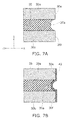
- FIGS. 7A to 8B show magnification of the region 7 A shown in FIG. 6 .
- the selection element 50 is formed above the global bit line 10 ; and a stacked body 80 is formed above the selection element 50 .
- the stacked body 80 includes conductive films 33 and inter-layer insulating films 35 .
- the conductive films 33 are, for example, conductive polycrystalline silicon films, or metal films; and the inter-layer insulating films 35 are, for example, silicon oxide films.
- the conductive films 33 and the inter-layer insulating films 35 are stacked alternately.
- a trench 65 is made to divide the stacked body 80 .
- the trench 65 is formed using RIE (Reactive Ion Etching) method, for example, so as to extend in the Y-direction. Thereby, the conductive films 33 are divided into the word lines 30 .
- RIE Reactive Ion Etching
- the inter-layer insulating film 35 that is exposed between the word lines 30 a and 30 b at the inner surface of the trench 65 is etched so that the end surface 35 a of the inter-layer insulating film 35 is recessed in the ⁇ X direction.
- the end surface of the inter-layer insulating film 35 that is exposed at the inner wall of the trench 65 is recessed, comparing to the end surfaces 30 e and 30 f of the word lines 30 .
- the end surface of the inter-layer insulating film 35 may be recessed by using a selective etching of the inter-layer insulating film 35 , for example, by using dilute hydrofluoric acid (wet etching).
- an insulating film 43 is formed at the inner surface of the trench 65 .
- the insulating film 43 can be formed conformally on the inner surface of the trench 65 .
- the insulating film 43 is, for example, a silicon oxide film and is formed by ALD (Atomic Layer Deposition). As shown in this drawing, the insulating film 43 continuously covers the end surfaces 30 e and 30 f of the word lines 30 and the end surface 35 a of the inter-layer insulating film 35 .
- variable resistance film 40 is formed on the insulating film 43 at the inner surface of the trench 65 .
- the variable resistance film 40 includes, for example, an oxide of at least one element selected from the group consisting of hafnium (Hf), zirconium (Zr), nickel (Ni), tantalum (Ta), tungsten (W), cobalt (Co), aluminum (Al), iron (Fe), manganese (Mn), chrome (Cr), and niobium (Nb).
- the metallic element included in the variable resistance film 40 is diffused into the insulating film 43 by performing heat treatment of the insulating film 43 and the variable resistance film 40 .
- the insulating film 43 changes into the insulating film 45 that includes the same metallic element as the variable resistance film 40 .
- the insulating film 45 also includes hafnium.
- the local bit line 20 is formed by filling a conductor 20 a into the interior of the trench 65 .
- the local bit line 20 is electrically connected to, for example, the source-drain unit 59 of the selection element 50 .
- FIG. 9B is a top-view drawing of the upper surface (in-plan direction) of the memory cell array 2 in which the local bit line 20 is formed.
- the conductor 20 a which is the material of the local bit line 20 is, for example, conductive polycrystalline silicon.
- the conductor 20 a is subdivided into substantially columnar bodies extending in the Z-direction. Each columnar body serves as the local bit line 20 ; and an insulator 67 is filled between the local bit lines 20 arranged in the Y-direction.
- the insulator 67 is, for example, a silicon oxide film.
- the conductors 20 a are etched into the substantially columnar bodies by using, for example, RIE method.
- selectivity of the etching is preferably set to be high between the variable resistance film 40 and the conductors 20 a .
- the variable resistance film 40 protects the word lines 30 so as to suppress damages therein.
- FIG. 9C is a cross-sectional drawing of part 9 c of the memory cell array 2 , which has the same structure as the one explained in reference to FIG. 5 .
- the manufacturing processes are simplified in the method according to the embodiment. Also, the parasitic capacitance between the word lines 30 can be reduced, because the inter-layer insulating film 35 does not include a high dielectric constant film.
Landscapes
- Engineering & Computer Science (AREA)
- Manufacturing & Machinery (AREA)
- Chemical & Material Sciences (AREA)
- Materials Engineering (AREA)
- Semiconductor Memories (AREA)
Abstract
Description
Claims (14)
Priority Applications (2)
| Application Number | Priority Date | Filing Date | Title |
|---|---|---|---|
| US14/208,204 US9224788B2 (en) | 2013-11-29 | 2014-03-13 | Nonvolatile memory device and method for manufacturing same |
| JP2014112438A JP2015106708A (en) | 2013-11-29 | 2014-05-30 | Nonvolatile memory device |
Applications Claiming Priority (2)
| Application Number | Priority Date | Filing Date | Title |
|---|---|---|---|
| US201361910164P | 2013-11-29 | 2013-11-29 | |
| US14/208,204 US9224788B2 (en) | 2013-11-29 | 2014-03-13 | Nonvolatile memory device and method for manufacturing same |
Publications (2)
| Publication Number | Publication Date |
|---|---|
| US20150155333A1 US20150155333A1 (en) | 2015-06-04 |
| US9224788B2 true US9224788B2 (en) | 2015-12-29 |
Family
ID=53265989
Family Applications (1)
| Application Number | Title | Priority Date | Filing Date |
|---|---|---|---|
| US14/208,204 Active US9224788B2 (en) | 2013-11-29 | 2014-03-13 | Nonvolatile memory device and method for manufacturing same |
Country Status (2)
| Country | Link |
|---|---|
| US (1) | US9224788B2 (en) |
| JP (1) | JP2015106708A (en) |
Cited By (3)
| Publication number | Priority date | Publication date | Assignee | Title |
|---|---|---|---|---|
| US10211259B2 (en) | 2016-06-23 | 2019-02-19 | Toshiba Memory Corporation | Semiconductor memory device and method of manufacturing the same |
| US10269433B2 (en) | 2017-09-19 | 2019-04-23 | Toshiba Memory Corporation | Memory device |
| US10522596B2 (en) | 2017-07-18 | 2019-12-31 | Toshiba Memory Corporation | Semiconductor storage device comprising resistance change film and method of manufacturing the same |
Families Citing this family (3)
| Publication number | Priority date | Publication date | Assignee | Title |
|---|---|---|---|---|
| US9865655B2 (en) * | 2015-12-15 | 2018-01-09 | Taiwan Semiconductor Manufacturing Co., Ltd. | Memory cell structure with resistance-change material and method for forming the same |
| US9947721B2 (en) | 2016-04-01 | 2018-04-17 | Micron Technology, Inc. | Thermal insulation for three-dimensional memory arrays |
| US10096652B2 (en) | 2016-09-12 | 2018-10-09 | Toshiba Memory Corporation | Semiconductor memory device |
Citations (13)
| Publication number | Priority date | Publication date | Assignee | Title |
|---|---|---|---|---|
| US20090189282A1 (en) | 2008-01-10 | 2009-07-30 | Rohm Co., Ltd. | Semiconductor device |
| JP2009188393A (en) | 2008-01-10 | 2009-08-20 | Rohm Co Ltd | Semiconductor device |
| JP2011129639A (en) | 2009-12-16 | 2011-06-30 | Toshiba Corp | Resistance change type memory cell array |
| US20110235408A1 (en) | 2010-03-24 | 2011-09-29 | Hitachi, Ltd. | Semiconductor memory device |
| US20120161094A1 (en) * | 2010-12-22 | 2012-06-28 | Chinese Academy of Science, Institute of Microelectronics | 3d semiconductor memory device and manufacturing method thereof |
| US20130034945A1 (en) | 2011-08-03 | 2013-02-07 | Samsung Electronics Co., Ltd. | Nonvolatile Memory Device and Method of Fabricating the Same |
| US20130240821A1 (en) * | 2012-03-19 | 2013-09-19 | Globalfoundries Singapore Pte Ltd | Three dimensional rram device, and methods of making same |
| US20130292630A1 (en) * | 2012-05-01 | 2013-11-07 | Hitachi, Ltd. | Semiconductor memory device |
| US20140027707A1 (en) * | 2011-07-07 | 2014-01-30 | Kabushiki Kaisha Toshiba | Memory device and fabricating method thereof |
| US20140061577A1 (en) * | 2012-08-31 | 2014-03-06 | Kabushiki Kaisha Toshiba | Semiconductor memory device and method of manufacturing the same |
| US8735860B2 (en) * | 2012-04-30 | 2014-05-27 | Samsung Electronics Co., Ltd. | Variable resistance memory device and method of fabricating the same |
| US20140369104A1 (en) * | 2011-12-07 | 2014-12-18 | Kabushiki Kaisha Toshiba | Memory device |
| US20150206580A1 (en) * | 2014-01-22 | 2015-07-23 | Kabushiki Kaisha Toshiba | Semiconductor memory device |
-
2014
- 2014-03-13 US US14/208,204 patent/US9224788B2/en active Active
- 2014-05-30 JP JP2014112438A patent/JP2015106708A/en active Pending
Patent Citations (15)
| Publication number | Priority date | Publication date | Assignee | Title |
|---|---|---|---|---|
| JP2009188393A (en) | 2008-01-10 | 2009-08-20 | Rohm Co Ltd | Semiconductor device |
| US20090189282A1 (en) | 2008-01-10 | 2009-07-30 | Rohm Co., Ltd. | Semiconductor device |
| US8299571B2 (en) | 2009-12-16 | 2012-10-30 | Kabushiki Kaisha Toshiba | Resistance-change memory cell array |
| JP2011129639A (en) | 2009-12-16 | 2011-06-30 | Toshiba Corp | Resistance change type memory cell array |
| US20110235408A1 (en) | 2010-03-24 | 2011-09-29 | Hitachi, Ltd. | Semiconductor memory device |
| JP2011199215A (en) | 2010-03-24 | 2011-10-06 | Hitachi Ltd | Semiconductor memory device |
| US20120161094A1 (en) * | 2010-12-22 | 2012-06-28 | Chinese Academy of Science, Institute of Microelectronics | 3d semiconductor memory device and manufacturing method thereof |
| US20140027707A1 (en) * | 2011-07-07 | 2014-01-30 | Kabushiki Kaisha Toshiba | Memory device and fabricating method thereof |
| US20130034945A1 (en) | 2011-08-03 | 2013-02-07 | Samsung Electronics Co., Ltd. | Nonvolatile Memory Device and Method of Fabricating the Same |
| US20140369104A1 (en) * | 2011-12-07 | 2014-12-18 | Kabushiki Kaisha Toshiba | Memory device |
| US20130240821A1 (en) * | 2012-03-19 | 2013-09-19 | Globalfoundries Singapore Pte Ltd | Three dimensional rram device, and methods of making same |
| US8735860B2 (en) * | 2012-04-30 | 2014-05-27 | Samsung Electronics Co., Ltd. | Variable resistance memory device and method of fabricating the same |
| US20130292630A1 (en) * | 2012-05-01 | 2013-11-07 | Hitachi, Ltd. | Semiconductor memory device |
| US20140061577A1 (en) * | 2012-08-31 | 2014-03-06 | Kabushiki Kaisha Toshiba | Semiconductor memory device and method of manufacturing the same |
| US20150206580A1 (en) * | 2014-01-22 | 2015-07-23 | Kabushiki Kaisha Toshiba | Semiconductor memory device |
Cited By (3)
| Publication number | Priority date | Publication date | Assignee | Title |
|---|---|---|---|---|
| US10211259B2 (en) | 2016-06-23 | 2019-02-19 | Toshiba Memory Corporation | Semiconductor memory device and method of manufacturing the same |
| US10522596B2 (en) | 2017-07-18 | 2019-12-31 | Toshiba Memory Corporation | Semiconductor storage device comprising resistance change film and method of manufacturing the same |
| US10269433B2 (en) | 2017-09-19 | 2019-04-23 | Toshiba Memory Corporation | Memory device |
Also Published As
| Publication number | Publication date |
|---|---|
| JP2015106708A (en) | 2015-06-08 |
| US20150155333A1 (en) | 2015-06-04 |
Similar Documents
| Publication | Publication Date | Title |
|---|---|---|
| US9224788B2 (en) | Nonvolatile memory device and method for manufacturing same | |
| US9059395B2 (en) | Resistive random access memory devices having variable resistance layers and related methods | |
| KR102789289B1 (en) | Semiconductor memory device and semiconductor device | |
| US9018613B2 (en) | Semiconductor memory device with a memory cell block including a block film | |
| US9997570B2 (en) | Resistive memory with varying dopant concentration in select transistor channel | |
| US10043822B2 (en) | Semiconductor memory devices having vertical pillars that are electrically connected to lower contacts | |
| CN112349774A (en) | Ferroelectric memory device having ferroelectric sensing layer and method of fabricating the same | |
| US9947685B2 (en) | 3D non-volatile memory array utilizing metal ion source | |
| JP6009971B2 (en) | Semiconductor memory device and manufacturing method thereof | |
| KR102373542B1 (en) | Semiconductor memory device | |
| JP2015133458A (en) | Nonvolatile semiconductor storage device | |
| US9583629B2 (en) | Semiconductor device | |
| US9748312B2 (en) | Semiconductor memory device | |
| TWI570722B (en) | Semiconductor memory device | |
| US9812507B2 (en) | Semiconductor memory device | |
| TWI644422B (en) | Semiconductor memory device | |
| US9905759B2 (en) | Memory device and method for manufacturing the same | |
| US9318532B2 (en) | Semiconductor memory device | |
| US9570514B2 (en) | Semiconductor device | |
| US10074694B2 (en) | Memory device and method for manufacturing the same | |
| US9728585B1 (en) | Semiconductor memory device | |
| US10050087B1 (en) | Semiconductor memory device | |
| US20170077180A1 (en) | Nonvolatile semiconductor memory device | |
| EP4712716A1 (en) | Semiconductor device | |
| US20160078910A1 (en) | Semiconductor memory device and driving method thereof |
Legal Events
| Date | Code | Title | Description |
|---|---|---|---|
| AS | Assignment |
Owner name: KABUSHIKI KAISHA TOSHIBA, JAPAN Free format text: ASSIGNMENT OF ASSIGNORS INTEREST;ASSIGNORS:KOBAYASHI, SHIGEKI;YAMAGUCHI, TAKESHI;YAMATO, MASAKI;AND OTHERS;SIGNING DATES FROM 20140404 TO 20140408;REEL/FRAME:032738/0473 |
|
| STCF | Information on status: patent grant |
Free format text: PATENTED CASE |
|
| AS | Assignment |
Owner name: TOSHIBA MEMORY CORPORATION, JAPAN Free format text: ASSIGNMENT OF ASSIGNORS INTEREST;ASSIGNOR:KABUSHIKI KAISHA TOSHIBA;REEL/FRAME:043709/0035 Effective date: 20170706 |
|
| MAFP | Maintenance fee payment |
Free format text: PAYMENT OF MAINTENANCE FEE, 4TH YEAR, LARGE ENTITY (ORIGINAL EVENT CODE: M1551); ENTITY STATUS OF PATENT OWNER: LARGE ENTITY Year of fee payment: 4 |
|
| AS | Assignment |
Owner name: K.K. PANGEA, JAPAN Free format text: MERGER;ASSIGNOR:TOSHIBA MEMORY CORPORATION;REEL/FRAME:055659/0471 Effective date: 20180801 Owner name: TOSHIBA MEMORY CORPORATION, JAPAN Free format text: CHANGE OF NAME AND ADDRESS;ASSIGNOR:K.K. PANGEA;REEL/FRAME:055669/0401 Effective date: 20180801 Owner name: KIOXIA CORPORATION, JAPAN Free format text: CHANGE OF NAME AND ADDRESS;ASSIGNOR:TOSHIBA MEMORY CORPORATION;REEL/FRAME:055669/0001 Effective date: 20191001 |
|
| MAFP | Maintenance fee payment |
Free format text: PAYMENT OF MAINTENANCE FEE, 8TH YEAR, LARGE ENTITY (ORIGINAL EVENT CODE: M1552); ENTITY STATUS OF PATENT OWNER: LARGE ENTITY Year of fee payment: 8 |