US9223169B2 - Display device - Google Patents
Display device Download PDFInfo
- Publication number
- US9223169B2 US9223169B2 US14/749,006 US201514749006A US9223169B2 US 9223169 B2 US9223169 B2 US 9223169B2 US 201514749006 A US201514749006 A US 201514749006A US 9223169 B2 US9223169 B2 US 9223169B2
- Authority
- US
- United States
- Prior art keywords
- light
- scattering member
- anisotropic scattering
- refractive index
- display device
- Prior art date
- Legal status (The legal status is an assumption and is not a legal conclusion. Google has not performed a legal analysis and makes no representation as to the accuracy of the status listed.)
- Active
Links
Images


Classifications
-
- G—PHYSICS
- G02—OPTICS
- G02F—OPTICAL DEVICES OR ARRANGEMENTS FOR THE CONTROL OF LIGHT BY MODIFICATION OF THE OPTICAL PROPERTIES OF THE MEDIA OF THE ELEMENTS INVOLVED THEREIN; NON-LINEAR OPTICS; FREQUENCY-CHANGING OF LIGHT; OPTICAL LOGIC ELEMENTS; OPTICAL ANALOGUE/DIGITAL CONVERTERS
- G02F1/00—Devices or arrangements for the control of the intensity, colour, phase, polarisation or direction of light arriving from an independent light source, e.g. switching, gating or modulating; Non-linear optics
- G02F1/01—Devices or arrangements for the control of the intensity, colour, phase, polarisation or direction of light arriving from an independent light source, e.g. switching, gating or modulating; Non-linear optics for the control of the intensity, phase, polarisation or colour
- G02F1/13—Devices or arrangements for the control of the intensity, colour, phase, polarisation or direction of light arriving from an independent light source, e.g. switching, gating or modulating; Non-linear optics for the control of the intensity, phase, polarisation or colour based on liquid crystals, e.g. single liquid crystal display cells
- G02F1/133—Constructional arrangements; Operation of liquid crystal cells; Circuit arrangements
- G02F1/1333—Constructional arrangements; Manufacturing methods
- G02F1/1335—Structural association of cells with optical devices, e.g. polarisers or reflectors
- G02F1/133504—Diffusing, scattering, diffracting elements
-
- G—PHYSICS
- G02—OPTICS
- G02B—OPTICAL ELEMENTS, SYSTEMS OR APPARATUS
- G02B5/00—Optical elements other than lenses
- G02B5/02—Diffusing elements; Afocal elements
- G02B5/0205—Diffusing elements; Afocal elements characterised by the diffusing properties
- G02B5/0257—Diffusing elements; Afocal elements characterised by the diffusing properties creating an anisotropic diffusion characteristic, i.e. distributing output differently in two perpendicular axes
-
- G—PHYSICS
- G02—OPTICS
- G02B—OPTICAL ELEMENTS, SYSTEMS OR APPARATUS
- G02B5/00—Optical elements other than lenses
- G02B5/02—Diffusing elements; Afocal elements
- G02B5/0273—Diffusing elements; Afocal elements characterized by the use
- G02B5/0278—Diffusing elements; Afocal elements characterized by the use used in transmission
-
- G—PHYSICS
- G02—OPTICS
- G02F—OPTICAL DEVICES OR ARRANGEMENTS FOR THE CONTROL OF LIGHT BY MODIFICATION OF THE OPTICAL PROPERTIES OF THE MEDIA OF THE ELEMENTS INVOLVED THEREIN; NON-LINEAR OPTICS; FREQUENCY-CHANGING OF LIGHT; OPTICAL LOGIC ELEMENTS; OPTICAL ANALOGUE/DIGITAL CONVERTERS
- G02F1/00—Devices or arrangements for the control of the intensity, colour, phase, polarisation or direction of light arriving from an independent light source, e.g. switching, gating or modulating; Non-linear optics
- G02F1/01—Devices or arrangements for the control of the intensity, colour, phase, polarisation or direction of light arriving from an independent light source, e.g. switching, gating or modulating; Non-linear optics for the control of the intensity, phase, polarisation or colour
- G02F1/13—Devices or arrangements for the control of the intensity, colour, phase, polarisation or direction of light arriving from an independent light source, e.g. switching, gating or modulating; Non-linear optics for the control of the intensity, phase, polarisation or colour based on liquid crystals, e.g. single liquid crystal display cells
- G02F1/133—Constructional arrangements; Operation of liquid crystal cells; Circuit arrangements
- G02F1/1333—Constructional arrangements; Manufacturing methods
- G02F1/1335—Structural association of cells with optical devices, e.g. polarisers or reflectors
- G02F1/133553—Reflecting elements
- G02F1/133555—Transflectors
-
- G—PHYSICS
- G02—OPTICS
- G02F—OPTICAL DEVICES OR ARRANGEMENTS FOR THE CONTROL OF LIGHT BY MODIFICATION OF THE OPTICAL PROPERTIES OF THE MEDIA OF THE ELEMENTS INVOLVED THEREIN; NON-LINEAR OPTICS; FREQUENCY-CHANGING OF LIGHT; OPTICAL LOGIC ELEMENTS; OPTICAL ANALOGUE/DIGITAL CONVERTERS
- G02F1/00—Devices or arrangements for the control of the intensity, colour, phase, polarisation or direction of light arriving from an independent light source, e.g. switching, gating or modulating; Non-linear optics
- G02F1/01—Devices or arrangements for the control of the intensity, colour, phase, polarisation or direction of light arriving from an independent light source, e.g. switching, gating or modulating; Non-linear optics for the control of the intensity, phase, polarisation or colour
- G02F1/13—Devices or arrangements for the control of the intensity, colour, phase, polarisation or direction of light arriving from an independent light source, e.g. switching, gating or modulating; Non-linear optics for the control of the intensity, phase, polarisation or colour based on liquid crystals, e.g. single liquid crystal display cells
- G02F1/133—Constructional arrangements; Operation of liquid crystal cells; Circuit arrangements
- G02F1/1333—Constructional arrangements; Manufacturing methods
- G02F1/1335—Structural association of cells with optical devices, e.g. polarisers or reflectors
- G02F1/13363—Birefringent elements, e.g. for optical compensation
- G02F1/133638—Waveplates, i.e. plates with a retardation value of lambda/n
-
- G—PHYSICS
- G02—OPTICS
- G02F—OPTICAL DEVICES OR ARRANGEMENTS FOR THE CONTROL OF LIGHT BY MODIFICATION OF THE OPTICAL PROPERTIES OF THE MEDIA OF THE ELEMENTS INVOLVED THEREIN; NON-LINEAR OPTICS; FREQUENCY-CHANGING OF LIGHT; OPTICAL LOGIC ELEMENTS; OPTICAL ANALOGUE/DIGITAL CONVERTERS
- G02F2203/00—Function characteristic
- G02F2203/02—Function characteristic reflective
Definitions
- the present disclosure relates to a display device, and more specifically to a display device including an image display unit provided with a sheet-like anisotropic scattering member.
- a reflective image display unit that displays an image by controlling the reflection ratio of external light or incident light.
- a reflective liquid crystal display panel for example, includes a reflecting electrode that reflects incident light.
- the reflective liquid crystal display panel displays an image by controlling the reflection ratio of incident light with a liquid crystal material layer. Since a display device including such a reflective image display unit uses incident light from outside to display an image, it is possible to save the power consumption and reduce in its weight and thickness. Such display devices are used for portable electronic apparatuses, for example.
- Such a display device including a reflective image display unit it is possible to increase the reflection ratio for a given observation point and thus compensate for the reduction of reflection ratio in color displaying, by imparting an angle dependency to the light scattering property or characteristics in a display area of the image display unit. It is also possible to prevent an image from being seen or observed at or from a point other than a given observation point.
- Japanese Patent Application Laid-open Nos. 2000-297110 and 2008-239757 describe an anisotropic scattering member with a plurality of areas having different refractive indexes which may be used for controlling a viewing angle of the display device.
- an adverse iridescence such as rainbow-colored glare may occur because of optical interference due to a microstructure of the anisotropic scattering member.
- a display quality may be deteriorated.
- a display device including a reflective image display unit having a sheet-like anisotropic scattering member, wherein the sheet-like anisotropic scattering member has a surface in which both a low refractive index area and a high refractive index area exist, the sheet-like anisotropic scattering member is disposed so that a light enters from a first surface of the sheet-like anisotropic scattering member and exits as scattered light from a second surface of the sheet-like anisotropic scattering member, when an extent of refractive index difference at a boundary or vicinity thereof between the low refractive index area and the high refractive index area is relatively large in the first surface and relatively small in the second surface, and the display device satisfies mathematical formulae, 0.7 ⁇ T ( ⁇ )/ T ( ⁇ ) ⁇ 1 ⁇ 0
- FIG. 1 is a schematic perspective view of a display device according to a first embodiment
- FIG. 2A is a schematic perspective view for explaining a configuration of a reflective image display unit
- FIG. 2B is a schematic sectional view for explaining a structure of an anisotropic scattering member according to the first embodiment
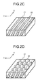
- FIG. 2C is a schematic perspective view for explaining arrangement of a low refractive index area and a high refractive index area in the anisotropic scattering member;
- FIG. 2D is a schematic perspective view for explaining another arrangement of the low refractive index area and the high refractive index area in the anisotropic scattering member;
- FIG. 3A is a schematic view for explaining a method for manufacturing the anisotropic scattering member according to the first embodiment
- FIG. 3B is another schematic view for explaining the method for manufacturing the anisotropic scattering member according to the first embodiment
- FIG. 4A is a schematic view for explaining a relation between incident light and scattered light in the anisotropic scattering member
- FIG. 4B is another schematic view for explaining the relation between incident light and scattered light in the anisotropic scattering member
- FIG. 5 is a schematic view for explaining a positional relation between the display device and an image observer when substantially parallel external light enters;
- FIG. 6A is a schematic sectional view of the reflective image display unit according to the first embodiment
- FIG. 6B is a schematic sectional view of a reflective image display unit according to a comparative embodiment
- FIG. 7 is a schematic view for explaining a relation between incident light and scattered light in the anisotropic scattering member
- FIG. 8 is a schematic view illustrating results obtained by measuring performance of the anisotropic scattering member
- FIG. 9A is a schematic view for explaining a relation between incident light and scattered light in the anisotropic scattering member
- FIG. 9B is another schematic view for explaining the relation between incident light and scattered light in the anisotropic scattering member
- FIG. 10A is a schematic view for explaining a relation between incident light and scattered light in the anisotropic scattering member
- FIG. 10B is another schematic view for explaining the relation between incident light and scattered light in the anisotropic scattering member
- FIG. 11 is still another schematic view for explaining the relation between incident light and scattered light in the anisotropic scattering member
- FIG. 12A is a schematic sectional view of a reflective image display unit according to a second embodiment
- FIG. 12B is a schematic sectional view of a reflective image display unit according to a comparative embodiment
- FIG. 13 is a schematic exploded perspective view of a reflective image display unit according to a third embodiment
- FIG. 14 is a schematic exploded perspective view of a reflective image display unit according to a fourth embodiment.
- FIG. 15 is a schematic sectional view of the reflective image display unit according to the fourth embodiment.
- An anisotropic scattering member transmits light entered from a predetermined direction and scatters light entered from another predetermined direction.
- the anisotropic scattering member may be disposed so that the scattered light is emitted when a light reflected in the image display unit passes through the anisotropic scattering member.
- the anisotropic scattering member may be disposed so that the scattered light is emitted when an incident light from outside passes through the anisotropic scattering member.
- the anisotropic scattering member can be formed with using a composition or the like containing a photoreactive compound.
- the anisotropic scattering member can be obtained in such a manner that a base material made of a composition whose refractive index changes to a certain extent before and after photopolymerization is irradiated with a light such as UV light from a predetermined direction.
- a base material made of a composition whose refractive index changes to a certain extent before and after photopolymerization is irradiated with a light such as UV light from a predetermined direction.
- appropriate materials whose refractive index changes to a certain extent between a photoreacted portion and the other portion can be selected from known photoreactive materials such as polymer or the like having a radical polymerizable functional group or a cation polymerizable functional group.
- the anisotropic scattering member also can be obtained in such a manner that a base material made of a composition for which a photoreactive compound and a non-photoreactive high molecular compound are mixed is irradiated with a light such as UV light from a predetermined direction.
- the non-photoreactive high molecular compound can be selected as appropriate from known materials such as acrylic resin, styrene resin and the like, for example.
- the base material made of aforementioned compositions can be obtained in such a manner that appropriate composition is applied on a polymer film base body by a known application method.
- both a low refractive index area and a high refractive index area exist in a surface of the anisotropic scattering member made from the aforementioned composition.
- a boundary between the low refractive index and the high refractive index forms a predetermined angle relative to a thickness direction of the anisotropic scattering member. Depending on the situation, it is possible to arrange the angle so that the angle continuously changes in the in-plane or surface direction.
- a surface irradiated with light is likely to be a surface where an extent of refractive index difference at a boundary or vicinity thereof between the low refractive index area and the high refractive index area is relatively large.
- an opposite surface is likely to be a surface where an extent of refractive index difference at a boundary or vicinity thereof between the low refractive index area and the high refractive index area is relatively small.
- the refractive index difference between the low refractive index area and the high refractive index area is preferably and usually not less than 0.01, more preferably not less than 0.05, and still more preferably not less than 0.10, in a vicinity of a surface where the refractive index difference at a boundary or vicinity thereof between the low refractive index area and the high refractive index area is relatively large.
- the anisotropic scattering member can be formed so that the photoreacted portion and the other portion take various shapes.
- the photoreacted portion and the other portion may take a louver-like shape or configuration.
- the photoreacted portion and the other portion may be formed as one or more column-like portions and a surrounding portion thereof.
- Examples of a reflective image display unit constituting the display device according to the present disclosure include, but are not limited to, a reflective liquid crystal display panel, etc.
- the image display unit may perform monochrome display or color display.
- the reflective liquid crystal display panel includes reflecting electrodes that reflect external light, for example.
- the reflective liquid crystal display panel displays an image by controlling the reflection ratio of external light with a liquid crystal material layer.
- the reflective liquid crystal display panel is formed of a front substrate provided with transparent common electrodes, a back substrate provided with pixel electrodes, and the liquid crystal material layer arranged between the front substrate and the back substrate, for example.
- the pixel electrodes themselves may be provided as reflecting electrodes and reflect light.
- a reflective film may reflect light in a combination of transparent pixel electrodes and the reflective film.
- An operating mode of the liquid crystal display panel is not particularly restricted as long as the operating mode does not interfere with a reflective display operation.
- the liquid crystal display panel may be driven in what is called a vertical alignment (VA) mode or an electrically controlled birefringence (ECB) mode, for example.
- VA vertical alignment
- EBC electrically controlled birefringence
- the image display unit may be formed of the reflective liquid crystal display panel.
- the reflective liquid crystal display panel includes the front substrate, the back substrate, and the liquid crystal material layer arranged between the front substrate and the back substrate.
- the anisotropic scattering member may be disposed on the front substrate side.
- the anisotropic scattering member may be formed by laminating a plurality of scattering members having different scattering characteristics.
- Transflective image display units having both reflective and transmissive characteristics are widely known, including a transflective liquid crystal display panel provided with both a reflective display area and a transmissive display area in a pixel, for example.
- the image display unit may be such a transflective image display unit.
- the “reflective image display unit” includes a “transflective image display unit”.
- the shape of the image display unit is not particularly restricted and may be a horizontally long rectangle or a vertically long rectangle.
- (M,N) denotes the number of pixels M ⁇ N in the image display unit
- a horizontally long rectangular image display unit may have some types of image display resolution, such as (640,480), (800,600), and (1024,768), as the value of (M,N), for example.
- a vertically long rectangular image display unit may have resolution obtained by switching the values described above, for example. The resolution is not limited to these values.
- a drive circuit that drives the image display unit may be formed of various circuits. These circuits may be formed using well-known circuit elements, for example.
- FIG. 1 is a schematic perspective view of the display device according to the first embodiment.
- a display device 100 includes a reflective image display unit 1 having a display area 11 in which pixels 12 are arrayed.
- the image display unit 1 is formed of a reflective liquid crystal display panel and is incorporated in a housing 40 .
- the image display unit 1 is driven by a drive circuit, which is not illustrated, for example.
- a part of the housing 40 is cut out.
- External light such as sunlight, enters the display area 11 .
- an assumption is made that the display area 11 is parallel to the X-Y plane and that the side from which an image is observed is positioned in the +Z-direction.
- FIG. 2A is a schematic perspective view for explaining the configuration of the reflective image display unit.
- FIG. 2B is a schematic sectional view for explaining a structure of an anisotropic scattering member according to the first embodiment.
- FIG. 2C and FIG. 2D are schematic perspective views for explaining arrangement of a low refractive index area and a high refractive index area in the anisotropic scattering member.
- the anisotropic scattering member 20 serves as a part of the liquid crystal display panel and is disposed on the front substrate 18 side.
- the laminated body 30 illustrated in FIG. 2A is formed by laminating a quarter-wave plate 31 , a half-wave plate 32 , and a polarizing plate 33 illustrated in FIG. 6A .
- the image display unit 1 has a rectangular shape.
- the sides of the image display unit 1 are denoted by reference numerals of 13 A, 13 B, 13 C and 13 D.
- the side 13 C is a side on the front side, and the side 13 A is a side opposite to the side 13 C.
- the sides 13 A and 13 C have a length of approximately 12 cm, whereas the sides 13 B and 13 D have a length of approximately 16 cm, for example. These lengths are given as examples only.
- the anisotropic scattering member 20 is a sheet (a film) having a thickness of approximately 0.02 to 0.5 mm, for example. As illustrated in FIG. 2B , the surface of the anisotropic scattering member 20 is formed as a region in which a low refractive index area 21 and a high refractive index area 22 are mixed in a micron order. For convenience of illustration, FIG. 2A to FIG. 2D and other figures do not illustrate a transparent film serving as a base sheet of the anisotropic scattering member 20 , for example.
- the anisotropic scattering member 20 which will be described later in detail with reference to FIG. 6A , is disposed so that an external light enters from a first surface and the incident light scatters from a second surface.
- the first surface is a side where an extent of change of the refractive index is relatively large near a boundary between the low refractive index area 21 and the high refractive index area 22 .
- the second surface is a side where an extent of change of the refractive index is relatively small near a boundary between the low refractive index area 21 and the high refractive index area 22 .
- the anisotropic scattering member 20 is disposed so that the external light reflected inside of the image display unit 1 scatters when passing through the anisotropic scattering member 20 .
- the anisotropic scattering member 20 is formed of a composition or the like containing a photoreactive compound, for example.
- the anisotropic scattering member 20 may have a structure in which the low refractive index area 21 and the high refractive index area 22 are formed in a louver-like manner, for example.
- the anisotropic scattering member 20 may have a structure in which the high refractive index area 22 and the low refractive index area 21 form column-shaped areas and a peripheral area surrounding the column-shaped areas, respectively.
- a composition part which has been photoreacted transforms into the high refractive index area in a column-shaped manner.
- widths of the low refractive index areas 21 in the thickness direction and the widths of the high refractive index areas 22 in the thickness direction are depicted as constant in FIG. 2C , this is given as an example only.
- shapes of the column-shaped areas are depicted as the same in FIG. 2D , this is given as an example only.
- the low refractive index area 21 and the high refractive index area 22 are formed in an oblique direction such that the boundary between the low refractive index area 21 and the high refractive index area 22 forms an angle ⁇ with respect to the thickness direction (Z-direction) of the anisotropic scattering member 20 as illustrated in FIG. 2B to FIG. 2D .
- the angle ⁇ is set to a preferable value as appropriate depending on specifications of the anisotropic scattering member 20 , for example. In some cases, the angle ⁇ may be set to 0 degree.
- a scattering central axis S of the anisotropic scattering member 20 is inclined with respect to the normal direction (Z-axis direction) of the observation surface of the display device 100 .
- the scattering central axis S is an axis around which an anisotropic scattering characteristics of the incident light becomes substantially symmetrical.
- the scattering central axis S is an axis extending in an incident direction of the most scattering light.
- the scattering central axis S is inclined basically in the same direction as the extending direction of the low refractive index area 21 and the high refractive index area 22 .
- the inclination angle of the scattering central axis S may be the same as or different from the inclination angle of the extending direction of the low refractive index area 21 and the high refractive index area 22 .
- the azimuth in which the scattering central axis S is projected on the X-Y plane corresponds to a direction perpendicular to the direction in which the louver-like areas extend.
- the azimuth corresponds to a direction in which a shadow obtained by projecting the column-shaped area on the X-Y plane extends.
- the low refractive index area 21 and the high refractive index area 22 are each formed in a louver-like manner and that the direction in which the louver-like areas extend is parallel to the X-direction as illustrated in FIG. 2C .
- the high refractive index area 22 is described as an area in which a base material causes photoreaction, this is given as an example only.
- the area in which the base material causes photoreaction may be the low refractive index area 21 .
- FIG. 3A and FIG. 3B are schematic views for explaining a method for manufacturing the anisotropic scattering member according to the first embodiment.
- the anisotropic scattering member 20 can be manufactured by: coating a base substance, such as a polyethylene terephthalate (PET) film, with a photoreactive composition to obtain a base material 20 ; and irradiating the base material 20 ′ with light obliquely from a light irradiation device 50 through a mask 60 having openings 61 , for example.
- PET polyethylene terephthalate
- the base material 20 ′ may be irradiated with light without using the mask 60 .
- the surface of the base material 20 ′ irradiated with the light output from the light irradiation device 50 is referred to as A-surface, whereas the side opposite thereto is referred to as a B-surface.
- the A-surface irradiated with the light is a surface in which a change in the refractive index occurring near the boundary between the low refractive index area 21 and the high refractive index area 22 is relatively large as illustrated in FIG. 3B .
- the B-surface opposite thereto is a surface in which a change in the refractive index occurring near the boundary between the low refractive index area 21 and the high refractive index area 22 is relatively small.
- the angle of the irradiation light By adjusting the angle of the irradiation light, it is possible to set the angle ⁇ of the boundary between the low refractive index area 21 and the high refractive index area 22 with respect to the thickness direction (Z-direction) of the anisotropic scattering member 20 to various angles in the anisotropic scattering member 20 .
- the interval between the irradiation positions of the irradiation pattern it is possible to adjust the interval between the boundaries of the low refractive index area 21 and the high refractive index area 22 and the interval between the high refractive index area 22 and the high refractive index area 22 , for example.
- FIG. 4A and FIG. 4B are schematic views for explaining a relation between incident light and scattered light in the anisotropic scattering member.
- FIG. 4A and FIG. 4B are different from each other in the light incident directions.
- FIG. 5 is a schematic view for explaining a positional relation between the display device and an image observer when substantially parallel external light enters.
- an image observer observes an image at a position distant from the display area 11 by a distance LZ in the state where the incident direction of the external light and the normal direction of the image display unit 1 form an angle ⁇ .
- YD denotes the length of the surface inclined with respect to the incident direction of the external light by the angle ⁇ in the image display unit 1 .
- FIG. 6A is a schematic sectional view of the reflective image display unit according to the first embodiment.
- FIG. 6B is a schematic sectional view of a reflective image display unit according to a comparative embodiment.
- the reflecting electrodes 16 each have a mirror-like surface and are provided to respective pixels 12 .
- elements including thin film transistors (TFT) are coupled to the respective pixels 12 .
- FIG. 3A does not illustrate various wirings including the TFTs and the signal lines.
- the liquid crystal material layer 17 is arranged between the front substrate 18 and the back substrate 14 .
- liquid crystal molecules 17 A are oriented in a predetermined direction.
- the liquid crystal material layer 17 has a thickness large enough to act as a half-wave plate when light is reciprocated by a spacer, which is not illustrated, in predetermined conditions, for example.
- the anisotropic scattering member 20 is disposed on the side opposite to the liquid crystal material layer 17 side of the front substrate 18 .
- the quarter-wave plate 31 , the half-wave plate 32 , and the polarizing plate 33 are arranged above the anisotropic scattering member 20 .
- An incident light entered from outside is formed into a linear polarized light with a predetermined direction through the polarizing plate 33 .
- the linear polarized light is formed into a circular polarized light through the half-wave plate 32 and the quarter-wave plate 31 .
- a combination of the half-wave plate 32 and the quarter-wave plate 31 functions as a broadband quarter-wave plate.
- the circular polarized light enters the scattering member 20 from a direction orthogonal or almost orthogonal to a direction in which a boundary between the low refractive index area 21 and the high refractive index area 22 extends. Therefore, the circular polarized light passes through the scattering member 20 without scattering, then passes through the liquid crystal material layer 17 , and reaches the reflecting electrode 16 .
- the light is reflected on the reflecting electrode 16 and passes through the liquid crystal material layer 17 .
- the light enters from A-surface and exits from B-surface of the anisotropic scattering member 20 . Since the light enters the scattering member 20 from a direction along or substantially along a direction in which a boundary between the low refractive index area 21 and the high refractive index area 22 extends, the light exits as scattered light from the scattering member 20 . However, since the scattered light exits from a surface where an extent of refractive index difference at a boundary or vicinity thereof between the low refractive index area 21 and the high refractive index area 22 is relatively small, the iridescence caused by optical interference due to a microstructure is reduced.
- the scattered light reaches the polarizing plate 33 through the quarter-wave plate 31 and the half-wave plate 32 .
- the light emits toward outside. It is possible to control an amount of the light which is reflected by the reflecting electrode 16 and passing through the polarizing plate 33 , by controlling an electric voltage applied to the reflecting electrode 16 or the like and thus controlling the alignment state of the liquid crystal molecular 17 A in the liquid crystal material layer 17 .
- the anisotropic scattering member is disposed so that a light enters from A-surface and exits as scattered light from B-surface, when an extent of refractive index difference at a boundary or vicinity thereof between the low refractive index area and the high refractive index area is relatively large in A-surface and relatively small in B-surface. More specifically, the anisotropic scattering member is disposed so that a light is scattered when the light reflected in the image display unit passes through the anisotropic scattering member toward outside. Since the light is scattered when exiting from the surface where an extent of refractive index difference at a boundary or vicinity thereof between the low refractive index area and the high refractive index area is relatively small, the iridescence (ex. rainbow-colored glare) caused by optical interference due to a microstructure can be reduced.
- ⁇ denotes a scattering angular range
- ⁇ denotes a main incident angle of set light
- T(a) denotes transmittance at a position on an extension line in the incident direction of the light at an incident angle a
- the main incident angle ⁇ satisfies ⁇ 0
- the anisotropic scattering member 20 satisfies 0.7 ⁇ T( ⁇ )/T( ⁇ ) ⁇ 1.
- the main incident angle ⁇ is an angle at which external light La is set to be incident in designing.
- the main incident angle ⁇ is 0 when the external light La enters perpendicularly (vertically) to the surface of the anisotropic scattering member 20 .
- a direction in which the main incident angle ⁇ rotates closer to the image observer from the vertical direction corresponds to a positive direction, whereas a direction in which the main incident angle ⁇ rotates away from the image observer from the vertical direction corresponds to a negative direction.
- the main incident angle ⁇ has a negative value.
- the scattering angular range 2 ⁇ is an angular range in which incident light can be scattered when the light enters the anisotropic scattering member 20 at various angles as the main incident angle ⁇ . Specifically, when light enters at a central angle of an angular unit that scatters light in the anisotropic scattering member 20 , the anisotropic scattering member 20 outputs light spreading out at an angle ⁇ in the positive direction with respect to the incident angle and at an angle ⁇ in the negative direction.
- the scattering angular range 2 ⁇ is also an angular range in which transmittance is reduced. The transmittance is measured for each angle at a position on an extension line in the incident direction of the light when the light enters.
- the angular range in which the transmittance is reduced corresponds to a range in which the incident light does not pass through the anisotropic scattering member 20 without any change.
- the angular range in which the transmittance is reduced is an angular range in which the incident light is scattered.
- the scattering angular range 2 ⁇ is an angular range in which the incident light is scattered.
- the external light La incident at the main incident angle ⁇ of a negative angle passes through the anisotropic scattering member 20 and is reflected by the reflecting electrode 16 .
- the external light La then passes through the anisotropic scattering member 20 again and is output from the display device 1 .
- Light Lb is output at an angle ⁇ (an angle ⁇ in the positive direction) among the light that is reflected by the reflecting electrode 16 , passes through the anisotropic scattering member 20 again, and is output from the display device 1 .
- the light Lb is light not being scattered among the external light La.
- Light Lc is output at an angle
- the light Lc is light rotated closer to the external light La side than the light Lb by an angle ⁇ .
- the light Lc corresponds to an end on the external light La side in the case where the external light La incident at the main incident angle ⁇ is scattered in the widest range by the anisotropic scattering member 20 .
- T(a) denotes the transmittance at a position on the extension line in the incident direction of the light obtained when the light enters the anisotropic scattering member 20 at the incident angle a.
- the distribution of the transmittance in the anisotropic scattering member 20 was measured.
- FIG. 8 illustrates the measurement result.
- the abscissa represents an angle (deg)
- the ordinate represents transmittance (Y) (%) at a position rotated with respect to the incident angle by 180 degrees.
- FIG. 8 also illustrates a measurement result of transmittance distribution in another anisotropic scattering member having different characteristics as a comparative example. The transmittance distribution with which iridescence is seen in FIG.
- FIG. 8 is the distribution of the transmittance T(a) in the anisotropic scattering member 20 according to the present embodiment.
- the transmittance distribution with which no iridescence is seen in FIG. 8 is the distribution of the transmittance T(a) in the anisotropic scattering member according to the comparative example.
- the main incident angle ⁇ is set to ⁇ 20° and the scattering angular range 2 ⁇ is set to 50° in the transmittance distribution illustrated in FIG. 8 .
- a part of the light incident as the external light La is reflected to be the light Lb of an angle of 20° ( ⁇ ), whereas another part thereof is reflected to be the light Lc of an angle of ⁇ 5° (
- the anisotropic scattering member 20 according to the present embodiment satisfies 0.7 ⁇ T( ⁇ )/T( ⁇ ) ⁇ 1, thereby making the transmittance of the light Lc and the transmittance of the light La equivalent.
- T( ⁇ ) and T( ⁇ ) are portions having lower transmittance than other portions (portions with a larger angle), that is, a range in which the light is scattered.
- diffracted light diffiffraction light. This can suppress occurrence of iridescence at the angle
- the light Lb is regular reflection light having relatively high intensity compared with other angles. The regular reflection light can also be scattered appropriately.
- the anisotropic scattering member according to the comparative example does not satisfy 0.7 ⁇ T( ⁇ )/T( ⁇ ) ⁇ 1, thereby making the transmittance of the light Lc higher than the transmittance of the light La. Because the light Lc output at the angle
- the anisotropic scattering member when satisfying 0.7 ⁇ T( ⁇ )/T( ⁇ ) ⁇ 1, can suppress occurrence of iridescence at a position rotated on the incident light side with respect to the regular reflection light having relatively high intensity by a predetermined angle, that is, at a position away from the regular reflection light by the angle ⁇ . This can reduce the risk that the image observer observes iridescence, thereby displaying a more preferable image to the image observer. Suppression of occurrence of iridescence at the angle ⁇ can suppress occurrence of iridescence on the perpendicular line side of the display surface in which iridescence is made more conspicuous.
- the relation between the transmittance T( ⁇ ) and the transmittance T( ⁇ ) needs to satisfy 0.7 ⁇ T( ⁇ )/T( ⁇ ) ⁇ 1.
- the main incident angle ⁇ is preferably set to ⁇ 40° to ⁇ 20° inclusive in the anisotropic scattering member 20 .
- Setting the main incident angle to ⁇ 40° to ⁇ 20° inclusive can make the angle of the regular reflection light Lb having high intensity 20° to 40° inclusive. This makes it possible to output regular reflection light in a range of 20° to 40° inclusive serving as a range in which the image observer normally observes an image.
- Setting the main incident angle to ⁇ 40° to ⁇ 20° inclusive can prevent the visual line direction of the image observer from significantly deviating from the normal line of the image display unit 1 when a light source is present just above the image display unit 1 , for example. This makes it possible to output brighter light in the range in which the image observer normally observes an image.
- the relation between the main incident angle ⁇ and the scattering angular range 2 ⁇ preferably satisfies
- ⁇ 0 When
- the scattering angular range 2 ⁇ is preferably set equal to or larger than 50° in the anisotropic scattering member 20 . More preferably, the scattering angular range 2 ⁇ is set to 50° to 90° inclusive in the anisotropic scattering member 20 . This makes it possible to scatter light at the angle ⁇ and the angle ⁇ appropriately.
- a second embodiment also relates to a display device according to the present disclosure.
- the second embodiment is different from the first embodiment in that an anisotropic scattering member is arranged so as to scatter external light incident from the outside while the light is passing through the anisotropic scattering member.
- an anisotropic scattering member 20 is arranged as follows: external light enters from the surface in which a change in the refractive index occurring near the boundary between a low refractive index area 21 and a high refractive index area 22 is relatively large; and the light exits as scattered light from the surface in which a change in the refractive index occurring near the boundary between the low refractive index area 21 and the high refractive index area 22 is relatively small.
- the anisotropic scattering member 20 is arranged so as to scatter external light incident from the outside while the light is passing through the anisotropic scattering member 20 .
- the following describes behavior of light in the image display unit 2 in the state where the incident direction of the external light and the normal direction of the image display unit 2 form an angle ⁇ with reference to FIG. 12A .
- the external light incident from the outside passes through a polarizing plate 33 , a half-wave plate 32 , and a quarter-wave plate 31 , and enters the anisotropic scattering member 20 .
- the anisotropic scattering member 20 is arranged such that the direction in which the boundary between the low refractive index area 21 and the high refractive index area 22 extends is substantially along the incident light.
- the external light enters an A-surface and exits as scattered light from a B-surface.
- the light thus scattered passes through a liquid crystal material layer 17 , is reflected by reflecting electrode 16 , and passes through the liquid crystal material layer 17 again.
- the light is then incident on the B-surface of the anisotropic scattering member 20 and exits from the A-surface. Because the light enters in a direction substantially perpendicular to the direction in which the boundary between the low refractive index area 21 and the high refractive index area 22 extends, the light passes through the anisotropic scattering member 20 without any change.
- the light passes through the quarter-wave plate 31 and the half-wave plate 32 and reaches the polarizing plate 33 . The light then exits to the outside.
- the anisotropic scattering member 20 is arranged so as to scatter the external light incident from the outside while the light is passing through the anisotropic scattering member.
- the light exits as scattered light from the surface in which a change in the refractive index occurring near the boundary between the low refractive index area 21 and the high refractive index area 22 is relatively small. This reduces iridescent coloring due to light interference caused by the microstructure.
- the anisotropic scattering member 20 according to the second embodiment can reduce the risk that the image observer observes iridescence when satisfying 0.7 ⁇ T( ⁇ )/T( ⁇ ) ⁇ 1. This makes it possible to display a more preferable image to the image observer. Suppression of occurrence of iridescence at the angle ⁇ can suppress occurrence of iridescence on the perpendicular line side of the display surface in which iridescence is made more conspicuous.
- a third embodiment also relates to a display device according to the present disclosure.
- the structure of the scattering member 20 B is the same as that of the anisotropic scattering member 20 described in the first embodiment.
- the image display unit 3 is arranged such that the direction in which the louver structure is inclined in the scattering member 20 B is orthogonal to the direction in which the louver structure is inclined in the scattering member 20 A.
- the scattering member 20 A and the scattering member 20 B are different in the direction of the scattering central axis and in the shape of the area in which light is scattered.
- An anisotropic scattering member 320 is formed by laminating a plurality of scattering members having different scattering characteristics.
- Laminating a plurality of scattering members having different scattering characteristics can adjust the scattering range of light.
- an area in which light is scattered in the scattering member 20 A has an elliptical shape with its longitudinal axis extending along the Y-axis
- an area in which light is scattered in the scattering member 20 B has an elliptical shape with its longitudinal axis extending along the X-axis.
- the anisotropic scattering member 20 can reduce the risk that the image observer observes iridescence. This makes it possible to display a more preferable image to the image observer. Suppression of occurrence of iridescence at the angle ⁇ can suppress occurrence of iridescence on the perpendicular line side of the display surface in which iridescence is made more conspicuous.
- a fourth embodiment also relates to a display device according to the present disclosure.
- the fourth embodiment is different from the first embodiment in that an anisotropic scattering member is formed by laminating a plurality of scattering members having different scattering characteristics.
- a display device 400 according to the fourth embodiment has the same configuration as that of the first embodiment except for the structure of the anisotropic scattering member. Because the image display unit 1 in FIG. 1 can be considered as an image display unit 4 and the display device 100 can be considered as the display device 400 , a schematic perpendicular view of the display device 400 according to the fourth embodiment is not given. Because the image display unit 1 can be considered as the image display unit 4 by changing the anisotropic scattering member 20 in FIG. 2A as appropriate, a schematic perpendicular view for explaining the configuration of the image display unit 4 according to the fourth embodiment is not given.
- FIG. 14 is a schematic exploded perspective view illustrating the reflective image display unit according to the fourth embodiment.
- the image display unit 4 is formed by laminating a scattering member 20 A and a scattering member 20 C.
- the structure and the arrangement of the scattering member 20 A are the same as those of the anisotropic scattering member 20 described in the first embodiment.
- the structure of the scattering member 20 C is the same as that of the anisotropic scattering member 20 described in the first embodiment except for the value of the angle ⁇ illustrated in FIG. 2B .
- the image display unit 4 is arranged such that the direction in which the louver structure is inclined in the scattering member 20 C is along the direction in which the louver structure is inclined in the scattering member 20 A.
- the scattering member 20 A and the scattering member 20 C are different in the direction of the scattering central axis and in the shape of the area in which light is scattered.
- An anisotropic scattering member 420 is formed by laminating a plurality of scattering members having different scattering characteristics. Laminating a plurality of scattering members having different scattering characteristics can adjust the scattering range of light.
- the anisotropic scattering member 20 can reduce the risk that the image observer observes iridescence. This makes it possible to display a more preferable image to the image observer. Suppression of occurrence of iridescence at the angle ⁇ can suppress occurrence of iridescence on the perpendicular line side of the display surface in which iridescence is made more conspicuous.
- the first surface has a relatively large difference of refractive index between the low refractive index area and the high refractive index area
- the second surface has a relatively small difference of refractive index between the low refractive index area and the high refractive index area
- the display device satisfies mathematical formulae, 0.7 ⁇ T ( ⁇ )/ T ( ⁇ ) ⁇ 1 ⁇ 0 wherein 2 ⁇ represents a scattering angle range, ⁇ represents a predetermined main incident angle of light entering the scattering member, T(a) represents a transmittance at a position on an extension line of an incident direction of the light with an incident angle “a”.
- the main incident angle ⁇ is not less than ⁇ 40 degrees and not more than ⁇ 20 degrees.
- the sheet-like anisotropic scattering member satisfies a relationship represented by a mathematical formula,
- the scattering angle range 2 ⁇ is not less than 50 degrees and not more than 90 degrees.
- the sheet-like anisotropic scattering member is disposed so that the scattered light is emitted when a light reflected in the image display unit passes through the sheet-like anisotropic scattering member.
- the sheet-like anisotropic scattering member is disposed so that the scattered light is emitted when an incident light from outside passes through the sheet-like anisotropic scattering member.
- the sheet-like anisotropic scattering member is disposed at a front substrate side of the reflective liquid crystal display panel.
- the sheet-like anisotropic scattering member includes a plurality of scattering members having different scattering characteristics, the plurality of scattering members being stacked or laminated.
Landscapes
- Physics & Mathematics (AREA)
- Nonlinear Science (AREA)
- General Physics & Mathematics (AREA)
- Optics & Photonics (AREA)
- Mathematical Physics (AREA)
- Chemical & Material Sciences (AREA)
- Crystallography & Structural Chemistry (AREA)
- Liquid Crystal (AREA)
- Optical Elements Other Than Lenses (AREA)
- Devices For Indicating Variable Information By Combining Individual Elements (AREA)
Abstract
Description
0.7<T(θ−φ)/T(θ)≦1
θ<0
0.7<T(θ−φ)/T(θ)≦1
θ<0
0.7<T(θ−φ)/T(θ)≦1
θ<0
wherein 2φ represents a scattering angle range, θ represents a predetermined main incident angle of light entering the scattering member, T(a) represents a transmittance at a position on an extension line of an incident direction of the light with an incident angle “a”.
(2). The display device according to (1), wherein
|θ|−φ<0
wherein θ represents the main incident angle and 2φ represents the scattering angle range.
(4). The display device according to (1), wherein
Claims (13)
0.7<T(θ−φ)/T(θ)≦1
θ<0
|θ|−φ<0.
Priority Applications (2)
| Application Number | Priority Date | Filing Date | Title |
|---|---|---|---|
| US14/749,006 US9223169B2 (en) | 2013-01-16 | 2015-06-24 | Display device |
| US14/945,719 US20160077374A1 (en) | 2013-01-16 | 2015-11-19 | Display device |
Applications Claiming Priority (4)
| Application Number | Priority Date | Filing Date | Title |
|---|---|---|---|
| JP2013005817A JP2014137467A (en) | 2013-01-16 | 2013-01-16 | Display device |
| JP2013-005817 | 2013-01-16 | ||
| US14/155,872 US9091877B2 (en) | 2013-01-16 | 2014-01-15 | Display device |
| US14/749,006 US9223169B2 (en) | 2013-01-16 | 2015-06-24 | Display device |
Related Parent Applications (1)
| Application Number | Title | Priority Date | Filing Date |
|---|---|---|---|
| US14/155,872 Continuation US9091877B2 (en) | 2013-01-16 | 2014-01-15 | Display device |
Related Child Applications (1)
| Application Number | Title | Priority Date | Filing Date |
|---|---|---|---|
| US14/945,719 Continuation US20160077374A1 (en) | 2013-01-16 | 2015-11-19 | Display device |
Publications (2)
| Publication Number | Publication Date |
|---|---|
| US20150293400A1 US20150293400A1 (en) | 2015-10-15 |
| US9223169B2 true US9223169B2 (en) | 2015-12-29 |
Family
ID=51164876
Family Applications (3)
| Application Number | Title | Priority Date | Filing Date |
|---|---|---|---|
| US14/155,872 Expired - Fee Related US9091877B2 (en) | 2013-01-16 | 2014-01-15 | Display device |
| US14/749,006 Active US9223169B2 (en) | 2013-01-16 | 2015-06-24 | Display device |
| US14/945,719 Abandoned US20160077374A1 (en) | 2013-01-16 | 2015-11-19 | Display device |
Family Applications Before (1)
| Application Number | Title | Priority Date | Filing Date |
|---|---|---|---|
| US14/155,872 Expired - Fee Related US9091877B2 (en) | 2013-01-16 | 2014-01-15 | Display device |
Family Applications After (1)
| Application Number | Title | Priority Date | Filing Date |
|---|---|---|---|
| US14/945,719 Abandoned US20160077374A1 (en) | 2013-01-16 | 2015-11-19 | Display device |
Country Status (5)
| Country | Link |
|---|---|
| US (3) | US9091877B2 (en) |
| JP (1) | JP2014137467A (en) |
| KR (1) | KR20140092784A (en) |
| CN (1) | CN103969870A (en) |
| TW (1) | TWI524119B (en) |
Families Citing this family (14)
| Publication number | Priority date | Publication date | Assignee | Title |
|---|---|---|---|---|
| JP5826676B2 (en) | 2012-03-06 | 2015-12-02 | 株式会社ジャパンディスプレイ | Display device |
| KR20150095976A (en) * | 2014-02-13 | 2015-08-24 | 삼성디스플레이 주식회사 | Liquid crystal display device |
| CN104503129B (en) * | 2014-12-30 | 2018-02-13 | 京东方科技集团股份有限公司 | A kind of optics module and reflection display device |
| KR20160116162A (en) | 2015-03-26 | 2016-10-07 | 삼성디스플레이 주식회사 | Display apparatus |
| KR102639294B1 (en) | 2016-08-18 | 2024-02-21 | 삼성디스플레이 주식회사 | Liquid crystal display |
| JP6993976B2 (en) * | 2016-09-14 | 2022-01-14 | 株式会社巴川製紙所 | Light diffusion film laminate for reflective display device and reflective display device using this |
| TWI759451B (en) | 2017-03-31 | 2022-04-01 | 日商巴川製紙所股份有限公司 | Light guiding laminate using anisortropic optical film and planar light source device using the same |
| KR102416575B1 (en) * | 2017-07-04 | 2022-07-11 | 삼성디스플레이 주식회사 | Display device |
| EP3658981B1 (en) * | 2017-07-25 | 2025-09-10 | Barco N.V. | Front-lit reflective display |
| JP7245004B2 (en) * | 2018-06-20 | 2023-03-23 | リンテック株式会社 | Light diffusion control laminate and reflective display |
| US11341925B2 (en) | 2019-05-02 | 2022-05-24 | Dell Products L.P. | Information handling system adapting multiple display visual image presentations |
| US11017742B2 (en) * | 2019-05-02 | 2021-05-25 | Dell Products L.P. | Information handling system multiple display viewing angle brightness adjustment |
| TWI855163B (en) * | 2019-12-06 | 2024-09-11 | 日商琳得科股份有限公司 | Reflective display |
| DE102021130835A1 (en) * | 2021-11-24 | 2023-05-25 | Bayerische Motoren Werke Aktiengesellschaft | Projection display system for a vehicle |
Citations (2)
| Publication number | Priority date | Publication date | Assignee | Title |
|---|---|---|---|---|
| JP2000297110A (en) | 1999-04-15 | 2000-10-24 | Toppan Printing Co Ltd | Composition for anisotropic light scattering film |
| JP2008239757A (en) | 2007-03-27 | 2008-10-09 | Sumitomo Chemical Co Ltd | Photocurable composition and light control film obtained by curing the same |
Family Cites Families (11)
| Publication number | Priority date | Publication date | Assignee | Title |
|---|---|---|---|---|
| US6424395B1 (en) * | 1998-04-08 | 2002-07-23 | Toppan Printing Co., Ltd. | Light scattering film and liquid crystal display device |
| JP2003139963A (en) * | 2001-11-07 | 2003-05-14 | Toppan Printing Co Ltd | Light diffuser, front lighting device, and liquid crystal display device to which front lighting device is applied |
| JP2003295167A (en) * | 2002-04-01 | 2003-10-15 | Toppan Printing Co Ltd | Liquid crystal display |
| CN1227969C (en) * | 2003-07-07 | 2005-11-23 | 福建省诏安县绿洲生化有限公司 | Water quality modifier for aquaculture made from bagasse, and mfg. method and use thereof |
| JP2005050654A (en) * | 2003-07-28 | 2005-02-24 | Clariant Internatl Ltd | Surface light source |
| JP2006330033A (en) * | 2005-05-23 | 2006-12-07 | Toppan Printing Co Ltd | Resin composition for anisotropic light scattering film and anisotropic light scattering film |
| JP5926941B2 (en) * | 2010-12-15 | 2016-05-25 | リンテック株式会社 | Anisotropic light diffusion film composition and anisotropic light diffusion film |
| JP2012155068A (en) * | 2011-01-25 | 2012-08-16 | Sony Mobile Display Corp | Display panel, display device and electronic apparatus |
| JP5730081B2 (en) * | 2011-03-08 | 2015-06-03 | 株式会社ジャパンディスプレイ | Display device |
| JP5749960B2 (en) * | 2011-03-30 | 2015-07-15 | 株式会社ジャパンディスプレイ | Display device and electronic device |
| JP5836847B2 (en) * | 2012-03-06 | 2015-12-24 | 株式会社ジャパンディスプレイ | Liquid crystal display |
-
2013
- 2013-01-16 JP JP2013005817A patent/JP2014137467A/en active Pending
-
2014
- 2014-01-15 CN CN201410018384.XA patent/CN103969870A/en active Pending
- 2014-01-15 US US14/155,872 patent/US9091877B2/en not_active Expired - Fee Related
- 2014-01-16 TW TW103101712A patent/TWI524119B/en active
- 2014-01-16 KR KR1020140005411A patent/KR20140092784A/en not_active Ceased
-
2015
- 2015-06-24 US US14/749,006 patent/US9223169B2/en active Active
- 2015-11-19 US US14/945,719 patent/US20160077374A1/en not_active Abandoned
Patent Citations (2)
| Publication number | Priority date | Publication date | Assignee | Title |
|---|---|---|---|---|
| JP2000297110A (en) | 1999-04-15 | 2000-10-24 | Toppan Printing Co Ltd | Composition for anisotropic light scattering film |
| JP2008239757A (en) | 2007-03-27 | 2008-10-09 | Sumitomo Chemical Co Ltd | Photocurable composition and light control film obtained by curing the same |
Also Published As
| Publication number | Publication date |
|---|---|
| KR20140092784A (en) | 2014-07-24 |
| US20160077374A1 (en) | 2016-03-17 |
| TWI524119B (en) | 2016-03-01 |
| JP2014137467A (en) | 2014-07-28 |
| US20140198287A1 (en) | 2014-07-17 |
| CN103969870A (en) | 2014-08-06 |
| TW201432357A (en) | 2014-08-16 |
| US9091877B2 (en) | 2015-07-28 |
| US20150293400A1 (en) | 2015-10-15 |
Similar Documents
| Publication | Publication Date | Title |
|---|---|---|
| US9223169B2 (en) | Display device | |
| KR101970019B1 (en) | Display device and anisotropic scatterer | |
| US10401672B2 (en) | Display device | |
| CN104583849B (en) | Liquid crystal display device | |
| CN103907053B (en) | Liquid crystal display device | |
| JP2013088555A (en) | Liquid crystal display device | |
| US10018755B2 (en) | Light diffusion member and display device | |
| CN104641283B (en) | Liquid crystal display device | |
| US20130329147A1 (en) | Liquid crystal panel and liquid crystal display | |
| US11561439B2 (en) | Liquid crystal display device | |
| JP6082078B2 (en) | Display device |
Legal Events
| Date | Code | Title | Description |
|---|---|---|---|
| AS | Assignment |
Owner name: JAPAN DISPLAY INC., JAPAN Free format text: ASSIGNMENT OF ASSIGNORS INTEREST;ASSIGNORS:TAMAKI, MASAYA;MITSUI, MASASHI;FUKUNAGA, YOKO;SIGNING DATES FROM 20140106 TO 20140107;REEL/FRAME:035950/0504 |
|
| FEPP | Fee payment procedure |
Free format text: PAYOR NUMBER ASSIGNED (ORIGINAL EVENT CODE: ASPN); ENTITY STATUS OF PATENT OWNER: LARGE ENTITY |
|
| STCF | Information on status: patent grant |
Free format text: PATENTED CASE |
|
| MAFP | Maintenance fee payment |
Free format text: PAYMENT OF MAINTENANCE FEE, 4TH YEAR, LARGE ENTITY (ORIGINAL EVENT CODE: M1551); ENTITY STATUS OF PATENT OWNER: LARGE ENTITY Year of fee payment: 4 |
|
| MAFP | Maintenance fee payment |
Free format text: PAYMENT OF MAINTENANCE FEE, 8TH YEAR, LARGE ENTITY (ORIGINAL EVENT CODE: M1552); ENTITY STATUS OF PATENT OWNER: LARGE ENTITY Year of fee payment: 8 |
|
| AS | Assignment |
Owner name: MAGNOLIA WHITE CORPORATION, JAPAN Free format text: ASSIGNMENT OF ASSIGNORS INTEREST;ASSIGNOR:JAPAN DISPLAY INC.;REEL/FRAME:072130/0313 Effective date: 20250625 |