US9217918B2 - Photomask, photomask manufacturing apparatus, and photomask manufacturing method - Google Patents
Photomask, photomask manufacturing apparatus, and photomask manufacturing method Download PDFInfo
- Publication number
- US9217918B2 US9217918B2 US14/017,506 US201314017506A US9217918B2 US 9217918 B2 US9217918 B2 US 9217918B2 US 201314017506 A US201314017506 A US 201314017506A US 9217918 B2 US9217918 B2 US 9217918B2
- Authority
- US
- United States
- Prior art keywords
- photomask
- face
- pattern
- convex portion
- transfer target
- Prior art date
- Legal status (The legal status is an assumption and is not a legal conclusion. Google has not performed a legal analysis and makes no representation as to the accuracy of the status listed.)
- Active, expires
Links
Images


Classifications
-
- G—PHYSICS
- G03—PHOTOGRAPHY; CINEMATOGRAPHY; ANALOGOUS TECHNIQUES USING WAVES OTHER THAN OPTICAL WAVES; ELECTROGRAPHY; HOLOGRAPHY
- G03F—PHOTOMECHANICAL PRODUCTION OF TEXTURED OR PATTERNED SURFACES, e.g. FOR PRINTING, FOR PROCESSING OF SEMICONDUCTOR DEVICES; MATERIALS THEREFOR; ORIGINALS THEREFOR; APPARATUS SPECIALLY ADAPTED THEREFOR
- G03F1/00—Originals for photomechanical production of textured or patterned surfaces, e.g., masks, photo-masks, reticles; Mask blanks or pellicles therefor; Containers specially adapted therefor; Preparation thereof
- G03F1/68—Preparation processes not covered by groups G03F1/20 - G03F1/50
- G03F1/70—Adapting basic layout or design of masks to lithographic process requirements, e.g., second iteration correction of mask patterns for imaging
-
- G—PHYSICS
- G03—PHOTOGRAPHY; CINEMATOGRAPHY; ANALOGOUS TECHNIQUES USING WAVES OTHER THAN OPTICAL WAVES; ELECTROGRAPHY; HOLOGRAPHY
- G03F—PHOTOMECHANICAL PRODUCTION OF TEXTURED OR PATTERNED SURFACES, e.g. FOR PRINTING, FOR PROCESSING OF SEMICONDUCTOR DEVICES; MATERIALS THEREFOR; ORIGINALS THEREFOR; APPARATUS SPECIALLY ADAPTED THEREFOR
- G03F1/00—Originals for photomechanical production of textured or patterned surfaces, e.g., masks, photo-masks, reticles; Mask blanks or pellicles therefor; Containers specially adapted therefor; Preparation thereof
- G03F1/22—Masks or mask blanks for imaging by radiation of 100nm or shorter wavelength, e.g. X-ray masks, extreme ultraviolet [EUV] masks; Preparation thereof
Definitions
- the embodiments of the present invention relate to a photomask, a photomask manufacturing apparatus, and a photomask manufacturing method.
- EUV exposure apparatus To produce a downscaled semiconductor device, an exposure apparatus using extreme ultra violet (EUV) light (hereinafter, also “EUV exposure apparatus”) has been developed.
- the EUV exposure apparatus includes a plurality of mirrors to perform exposure and transfer from a photomask to a semiconductor substrate being a transfer target substrate.
- the mirror reflectance of the EUV light is relatively low and thus a limit is set on the number of mirrors to suppress a reduction in a light amount of the EUV light reaching the semiconductor substrate.
- the number of mirrors is small, the flexibility of correcting a position difference (an overlay error) between a ground pattern of the semiconductor substrate and a transfer pattern to be exposed is reduced.
- high-order correction on overlay is difficult to perform and it is hard to enhance overlay accuracy associated with downscaling of the semiconductor device.
- FIG. 1 shows a configuration example of a photomask creation apparatus 100 according to a first embodiment
- FIGS. 2A and 2B are a plan view and a sectional view showing a configuration of the photomask PM according to the first embodiment
- FIG. 3 shows an EUV exposure apparatus 200 that performs exposure using the photomask PM according to the first embodiment
- FIG. 4 is a flowchart showing a method of creating the photomask PM according to the first embodiment
- FIGS. 5A and 5B are a plan view and a sectional view showing a configuration of the photomask PM according to a second embodiment.
- FIG. 6 is a flowchart showing a creation method of the photomask PM according to the second embodiment.
- an upper direction or “a lower direction” refers to a relative direction when a direction of a surface of a semiconductor substrate on which semiconductor elements are provided is assumed as “an upper direction”. Therefore, the term “upper direction” or “lower direction” occasionally differs from an upper direction or a lower direction based on a gravitational acceleration direction.
- a photomask according to the present embodiment is used to transfer a pattern to a transfer target substrate in a non-telecentric optical system.
- a mask substrate includes a first face having a pattern formed thereon and a second face on an opposite side from the first face.
- a convex portion or a concave portion is formed on the second face in order to correct a position difference in a transfer pattern occurring when the pattern is transferred to the transfer target substrate.
- the convex portion is formed of a material different from that of the mask substrate.
- FIG. 1 shows a configuration example of a photomask manufacturing apparatus 100 according to a first embodiment.
- the photomask manufacturing apparatus 100 manufactures a photomask PM to be used to transfer a pattern to a semiconductor substrate being a transfer target substrate in a non-telecentric optical system such as an EUV exposure apparatus.
- a non-telecentric optical system such as an EUV exposure apparatus.
- chief rays are not parallel to the optical axis. Therefore, a phenomenon in which the size of a transfer pattern varies on an image field (the transfer target substrate, for example) or in which an alignment of the transfer pattern is shifted occurs when an object (the photomask, for example) moves in the direction of the optical axis.
- the non-telecentric optical system is adopted on an object side on which the photomask is placed.
- an overlay error is corrected by purposely using this property of the non-telecentric optical system.
- the photomask manufacturing apparatus 100 includes a stage 10 , a spotter 20 serving as a level-difference formation unit, a laser generation unit 30 serving as a solidification unit, and a controller 40 .
- the photomask PM is mounted on the stage 10 .
- the photomask PM is mounted on the stage 10 .
- the stage 10 can freely move the photomask PM to form a convex portion at an arbitrary position on the second face F2 of the photomask PM.
- the spotter 20 serving as a level-difference formation unit supplies a material of the convex portion onto the second face F2 of the photomask PM.
- the material is not particularly limited and can be either a fluid material or a solid material.
- the method of supplying a fluid material is not particularly limited and can be any of dripping, coating, spraying, and the like.
- the method of supplying a solid material is not particularly limited and can be any of injection, sputtering, and the like. It is assumed hereinafter that the spotter 20 supplies a fluid material. In the first embodiment, the spotter 20 drips the fluid material on the second face F2.
- the fluid material can be, for example, coating carbon or resin containing metal and desirably has conductivity.
- the laser generation unit 30 serving as the solidification unit applies laser light to the fluid material dripped on the second face F2 to solidify the fluid material supplied onto the photomask PM.
- the solidification unit is not particularly limited as long as it solidifies the fluid material.
- the solidification unit can be, for example, a light source of IR (Infrared Radiation) light, visible light, UV (Ultraviolet) light, or the like, or a heat source.
- the method of solidifying the fluid material is not particularly limited and can be drying, sintering, or the like.
- the controller 40 controls the operation of the stage 10 , the amount of the fluid material dripped from the spotter 20 , the timing of the dripping, the application time of the laser from the laser generation unit 30 , and the like.
- FIGS. 2A and 2B are a plan view and a sectional view showing a configuration of the photomask PM according to the first embodiment.
- FIG. 2A is a plan view of the second face F2.
- FIG. 2B is a sectional view along a line B-B in FIG. 2A .
- the photomask PM is a photomask (a reticle, for example) used to transfer a pattern to a semiconductor substrate in a non-telecentric optical system as mentioned above.
- Convex portions 51 to 54 in FIGS. 2A and 2B are schematically shown and represented in an exaggerated manner than that of the actual convex portions.
- the photomask PM includes a mask substrate 50 and the convex portions 51 to 54 .
- the mask substrate 50 has the first face F1 and the second face F2 on the opposite side from the first face F1.
- a circuit pattern to be exposed and transferred to a semiconductor substrate is formed on the first face F1.
- the convex portions 51 to 54 are formed on the second face F2 to correct a position difference (an overlay error) in a transfer pattern occurring when the circuit pattern is transferred to a semiconductor substrate.
- the circuit pattern is a pattern on the photomask PM formed on the first face F1.
- the transfer pattern is a pattern transferred to the front face of a semiconductor substrate when the circuit pattern is exposed to the semiconductor substrate using the photomask PM.
- the overlay error is a horizontal difference in the transfer pattern with respect to a ground pattern formed on a semiconductor substrate W shown in FIG. 3 .
- the convex portions 51 to 54 are formed of a material different from that of the mask substrate 50 .
- the mask substrate 50 is formed of a glass material and the convex portions 51 to 54 are formed of carbon or resin.
- the convex portions 51 to 54 are formed by solidifying the fluid material dripped from the spotter 20 with the laser light from the laser generation unit 30 .
- the laser generation unit 30 can locally apply laser to a part of the second face F2 of the photomask PM. Therefore, the laser generation unit 30 can sinter the convex portions 51 to 54 without thermally treating the entire photomask PM.
- Planar shapes and heights (sizes of differences in levels) ⁇ Z1 and ⁇ Z2 of the convex portions 51 to 54 are determined to some extent by a dripping speed and a dripping amount of the fluid material dripped from the spotter 20 and a movement direction and a movement speed of the stage 10 while the spotter 20 supplies the fluid material.
- the convex portions 51 to 54 can have a layered structure as shown in FIGS. 2A and 2B .
- the photomask manufacturing apparatus 100 can perform again the supply of the fluid material and the solidification of the fluid material to form the convex portions 53 and 54 on the convex portions 51 and 52 , respectively.
- the laser generation unit 30 can apply laser to the convex portions 51 to 54 in an oxygen atmosphere, thereby scraping (burning off) the convex portions 51 to 54 .
- parts of the convex portions 51 to 54 can be removed by ashing using an ashing apparatus.
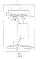
- FIG. 3 shows an EUV exposure apparatus 200 that performs exposure using the photomask PM according to the first embodiment.
- the EUV exposure apparatus 200 includes a vacuum chamber 1 , a reticle stage 7 , a wafer stage 8 , and an optical system 4 .
- the inside of the vacuum chamber 1 is maintained vacuum (a reduced-pressure atmosphere at about 1 ⁇ 10 ⁇ 4 pascal, for example).
- the reticle stage 7 , the wafer stage 8 , and the optical system 4 are provided in the vacuum chamber 1 and exposure with EUV light is performed in the vacuum chamber 1 .
- the reticle stage 7 has an electrostatic chuck and the photomask (that is, the reticle) PM is mounted thereon for exposure of the semiconductor substrate W.
- the reticle stage 7 is provided to be able to move in a scan direction during exposure.
- the electrostatic chuck of the reticle stage 7 adsorbs and fixes the photomask PM on the reticle stage 7 .
- the reticle stage 7 adsorbs the second face F2 (a rear face) of the photomask PM having the convex portions 51 to 54 formed thereon.
- a mount face of the reticle stage 7 is flat and is formed of a material with a high hardness, such as ceramic.
- the circuit pattern formed on the first face F1 has concavities and convexities.
- the wafer stage 8 has an electrostatic chuck and the semiconductor substrate W as an exposure target is mounted thereon.
- the wafer stage 8 is provided to be able to move in the scan direction during exposure.
- the electrostatic chuck of the wafer stage 8 fixes the semiconductor substrate W on the wafer stage 8 .
- the optical system 4 exposes and transfers the circuit pattern that is formed on the photomask PM mounted on the reticle stage 7 onto the semiconductor substrate W mounted on the wafer stage 8 .
- the optical system 4 exposes the semiconductor substrate W with exposure light reflected on the photomask PM. That is, the optical system 4 projects the pattern formed on the first face F1 of the photomask PM onto the semiconductor substrate W.
- a photosensitive material resist, for example
- EUV light exposure light
- the size of the differences in levels on the first face F1 extruded by the convex portions 51 to 54 (with heights of Z1 and Z2) of the photomask PM is ⁇ Z. It is assumed that an angle formed by a direction perpendicular to the first face F1 of the photomask PM and an incidence direction of the EUV light entering the photomask PM is ⁇ . It is assumed that a reduction ratio of the transfer pattern from the photomask PM onto the semiconductor substrate W in the optical system 4 is M. It is also assumed that a correction value (that is, an overlay correction value) of the position of the transfer pattern on the semiconductor substrate W depending on the size ⁇ Z of the level differences is ⁇ X. In this case, the following Expression 1 holds.
- ⁇ Z ⁇ X /( M ⁇ tan ⁇ ) (Expression 1) That is, the level differences ⁇ Z on the first face F1 of the photomask PM can shift (correct) the position of the transfer pattern on the semiconductor substrate W by ⁇ X. This can be rephrased as that the convex portions 51 to 54 formed on the second face F2 of the photomask PM can correct the position of the transfer pattern on the semiconductor substrate W.
- FIG. 4 is a flowchart showing a method of manufacturing the photomask PM according to the first embodiment.
- the photomask PM is manufactured as follows.
- a circuit pattern is first formed on the first face F1 of the photomask PM (Step S 10 ). Formation of the circuit pattern can be performed by an apparatus different from the photomask manufacturing apparatus 100 according to the first embodiment.
- Exposure is then performed using the photomask PM in the exposure apparatus 200 (Step S 20 ).
- the exposure apparatus 200 measures a position difference (an overlay error) in the transfer pattern on the semiconductor substrate W (Step S 30 ).
- the overlay error is preferably measured at a plurality of positions on a plane of the photomask PM.
- the overlay error can be measured at a plurality of grid points set in the plane of the photomask PM. In this way, the overlay error is evenly measured on the plane of the photomask PM.
- the photomask PM can be used as it is for production of a semiconductor device. Therefore, manufacturing of the photomask PM is ended.
- the photomask manufacturing apparatus 100 forms convex portions on the second face F2 of the photomask PM (Step S 50 ).
- the photomask manufacturing apparatus 100 determines formation positions of the convex portions, a supply amount of a fluid material, and the like according to a position on the photomask PM where the overlay error occurs, a measurement value of the overlay error, and the like.
- Expression 1 is used in this case assuming the overlay error as ⁇ X, the size ⁇ Z of a level difference required for correction can be calculated.
- a relation of the size ⁇ Z of the level difference on the first face F1 and the sizes ⁇ Z1 and ⁇ Z2 of the convex portions 51 to 54 and the positions thereof on the second face F2 can be previously set by a simulation such as a stress analysis, an empirical rule, or the like. Furthermore, the supply amount of the fluid material required to form the convex portions 51 to 54 with desired heights can be previously set by an empirical rule, or the like. It can be confirmed by a simulation that the convex portions expected to be formed can reduce the overlay error before actually forming the convex portions 51 to 54 . Furthermore, after the convex portions 51 to 54 are actually formed, the shapes such as the heights and sizes of the formed convex portions can be measured and then it can be confirmed by a simulation that the convex portions can reduce the overlay error.
- processes at Steps S 20 to S 40 are performed again.
- the processes at Steps S 20 to S 40 are repeated until the overlay error at each grid point falls within the standard range. In this way, the method according to the first embodiment can correct the overlay error.
- the number of repetitions of the processes at Steps S 20 to S 40 exceeds a predetermined value, re-creation of the circuit pattern itself of the photomask PM is conceivable.
- the photomask manufacturing apparatus and the photomask manufacturing method according to the first embodiment can correct an overlay error on the semiconductor substrate W by forming the convex portions 51 to 54 on the second face (the rear face) of the photomask PM.
- overlay accuracy in a ground pattern of the semiconductor substrate W and an exposed transfer pattern is enhanced, which results in an increased yield.
- an overlay error that cannot be corrected by the EUV exposure apparatus 200 can be corrected. That is, according to the first embodiment, high-order correction on overlay that cannot be performed by an EUV exposure apparatus can be achieved with the configuration of the photomask PM.
- FIGS. 5A and 5B are a plan view and a sectional view showing a configuration of the photomask PM according to a second embodiment.
- FIG. 5A is a plan view of the second face F2.
- FIG. 5B is a sectional view along a line B-B in FIG. 5A .
- the second embodiment is different from the first embodiment in that the photomask PM includes concave portions 61 to 64 instead of the convex portions.
- Other configurations of the photomask PM according to the second embodiment can be identical to those according to the first embodiment.
- the concave portions 61 to 64 can be formed by forming a new film with a uniform thickness on the second face F2 of the mask substrate 50 of the photomask PM and further etching the film.
- the film with the uniform thickness is formed by supplying a material of the film onto the second face F2 and solidifying the material.
- the material is not particularly limited and can be either a fluid material or a solid material.
- the supply method of the fluid material is not particularly limited and can be any of dripping, coating, and spraying.
- the fluid material can be, for example, coating carbon or resin containing metal and desirably has conductivity.
- the supply method of the solid material is not particularly limited and can be any of injection, sputtering, and the like.
- the solidification method of the material is not particularly limited and can be application of IR light, visible light, or UV light, drying, sintering, or the like.
- the photomask manufacturing apparatus can be an etching apparatus capable of etching a film formed on the second face F2.
- etching apparatus capable of etching a film formed on the second face F2.
- ⁇ Z in Expression 1 is the depth (the size of a level difference) of a concave portion on the first face F1 of the photomask PM.
- FIG. 6 is a flowchart showing a manufacturing method of the photomask PM according to the second embodiment.
- the photomask manufacturing apparatus determines formation positions or the like of the concave portions according to a position of the photomask PM at which an overlay error occurs, a measurement value of the overlay error, and the like.
- Expression 1 is used in this case assuming the overlay error as ⁇ X, the size ⁇ Z of a level difference required for correction can be calculated.
- a relation of the size ⁇ Z of the level difference on the first face F1 and the sizes ⁇ Z1 and ⁇ Z2 of the concave portions 61 to 64 and the positions thereof on the second face F2 can be previously set by a simulation such as a stress analysis, statistics, an empirical rule, or the like.
- the concave portions 61 to 64 can reduce the overlay error before actually forming the concave portions 61 to 64 .
- the shapes such as the heights and sizes of the formed concave portions can be measured and then it can be confirmed by a simulation that the concave portions can reduce the overlay error.
- a resist is formed on a film formed on the second face F2 of the photomask PM by using a lithography technique and then the resist is patterned.
- the etching apparatus then selectively etches the second face F2 of the photomask PM. Etching of the second face F2 can be either wet etching or dry etching. In this way, the concave portions can be formed on the second face F2 of the photomask PM.
- the processes at Steps S 20 to S 40 are performed again.
- the processes at Steps S 20 to S 40 are repeated until the overlay error at each grid point falls within the standard range. In this way, the method according to the second embodiment can correct the overlay error.
- the number of repetitions of the processes at Steps S 20 to S 40 exceeds a predetermined value, re-creation of the circuit pattern itself of the photomask PM is conceivable.
- the overlay error on the semiconductor substrate W can be corrected also by forming the concave portions 61 to 64 on the second face (the rear face) of the photomask PM.
- the second embodiment can achieve effects identical to those of the first embodiment.
- the photomask PM can include both of the convex portions and the concave portions on the second face F2. Accordingly, the overlay error can be corrected according to circumstances and the overlay accuracy can be further enhanced.
Landscapes
- Physics & Mathematics (AREA)
- General Physics & Mathematics (AREA)
- Exposure And Positioning Against Photoresist Photosensitive Materials (AREA)
- Preparing Plates And Mask In Photomechanical Process (AREA)
- Exposure Of Semiconductors, Excluding Electron Or Ion Beam Exposure (AREA)
Abstract
Description
ΔZ=ΔX/(M×tan θ) (Expression 1)
That is, the level differences ΔZ on the first face F1 of the photomask PM can shift (correct) the position of the transfer pattern on the semiconductor substrate W by ΔX. This can be rephrased as that the
Claims (18)
ΔZ=ΔX/(tan θ×M) (Expression 1)
ΔZ=ΔX/(tan θ×M) (Expression 1)
ΔZ=ΔX/(tan θ×M) (Expression 1)
ΔZ=ΔX/(tan θ×M) (Expression 1)
Applications Claiming Priority (2)
| Application Number | Priority Date | Filing Date | Title |
|---|---|---|---|
| JP2013-023555 | 2013-02-08 | ||
| JP2013023555A JP2014154721A (en) | 2013-02-08 | 2013-02-08 | Photomask, manufacturing device of photomask and method of manufacturing photomask |
Publications (2)
| Publication Number | Publication Date |
|---|---|
| US20140226138A1 US20140226138A1 (en) | 2014-08-14 |
| US9217918B2 true US9217918B2 (en) | 2015-12-22 |
Family
ID=51297239
Family Applications (1)
| Application Number | Title | Priority Date | Filing Date |
|---|---|---|---|
| US14/017,506 Active 2034-07-01 US9217918B2 (en) | 2013-02-08 | 2013-09-04 | Photomask, photomask manufacturing apparatus, and photomask manufacturing method |
Country Status (2)
| Country | Link |
|---|---|
| US (1) | US9217918B2 (en) |
| JP (1) | JP2014154721A (en) |
Families Citing this family (1)
| Publication number | Priority date | Publication date | Assignee | Title |
|---|---|---|---|---|
| DE102014218474A1 (en) * | 2014-09-15 | 2016-03-17 | Carl Zeiss Smt Gmbh | Projection objective, projection exposure apparatus and projection exposure method for EUV microlithography |
Citations (3)
| Publication number | Priority date | Publication date | Assignee | Title |
|---|---|---|---|---|
| JP2009177126A (en) | 2007-12-25 | 2009-08-06 | Nikon Corp | Mask blank, mask, mask holding apparatus, exposure apparatus, and device manufacturing method |
| JP2010122304A (en) | 2008-11-17 | 2010-06-03 | Dainippon Printing Co Ltd | Reflective mask blank, reflective mask, method for manufacturing reflective mask blank, and method for manufacturing reflective mask |
| US20120141927A1 (en) | 2010-12-06 | 2012-06-07 | Takashi Kamo | Reflective mask and method for manufacturing the same |
Family Cites Families (5)
| Publication number | Priority date | Publication date | Assignee | Title |
|---|---|---|---|---|
| JPH07295230A (en) * | 1994-04-25 | 1995-11-10 | Dainippon Screen Mfg Co Ltd | Alignment method of projected image for magnified projection type aligner |
| JP2000286191A (en) * | 1999-03-31 | 2000-10-13 | Nikon Corp | Exposure apparatus, exposure method, and device manufacturing method |
| JP2003007598A (en) * | 2001-06-25 | 2003-01-10 | Mitsubishi Electric Corp | Focus monitor method, focus monitor device, and semiconductor device manufacturing method |
| JP4239999B2 (en) * | 2005-05-11 | 2009-03-18 | セイコーエプソン株式会社 | Film pattern forming method, film pattern, device, electro-optical device, and electronic apparatus |
| JP4372178B2 (en) * | 2007-04-27 | 2009-11-25 | 株式会社東芝 | Light reflecting mask, light reflecting mask manufacturing method, and semiconductor device manufacturing method |
-
2013
- 2013-02-08 JP JP2013023555A patent/JP2014154721A/en active Pending
- 2013-09-04 US US14/017,506 patent/US9217918B2/en active Active
Patent Citations (4)
| Publication number | Priority date | Publication date | Assignee | Title |
|---|---|---|---|---|
| JP2009177126A (en) | 2007-12-25 | 2009-08-06 | Nikon Corp | Mask blank, mask, mask holding apparatus, exposure apparatus, and device manufacturing method |
| JP2010122304A (en) | 2008-11-17 | 2010-06-03 | Dainippon Printing Co Ltd | Reflective mask blank, reflective mask, method for manufacturing reflective mask blank, and method for manufacturing reflective mask |
| US20120141927A1 (en) | 2010-12-06 | 2012-06-07 | Takashi Kamo | Reflective mask and method for manufacturing the same |
| JP2012124214A (en) | 2010-12-06 | 2012-06-28 | Toshiba Corp | Reflective mask and method of manufacturing the same |
Non-Patent Citations (2)
| Title |
|---|
| Byounghoon Lee, et al., "Process Overlay Controllability in EUV Lithography", International Symposium on Extreme Ultraviolet Lithography, Process Optimization, Session 5, Oct. 2011, pp. 1-22. |
| S. Yoshitake, et al., "Desired IP Control methodology for EUV Mask in Current Mask Process", 24th European Mask and Lithography Conference, Proc. of SPIE, vol. 6792, Jun. 15, 2010, pp. 67920T-1-67920T-11. |
Also Published As
| Publication number | Publication date |
|---|---|
| US20140226138A1 (en) | 2014-08-14 |
| JP2014154721A (en) | 2014-08-25 |
Similar Documents
| Publication | Publication Date | Title |
|---|---|---|
| TWI776817B (en) | Location-specific tuning of stress to control bow to control overlay in semiconductor processing | |
| JP2018041080A5 (en) | ||
| TWI601619B (en) | Imprinting equipment and article manufacturing method | |
| US12099295B2 (en) | Imprint apparatuses and article manufacturing methods applying viscosity increases without curing of imprint material | |
| KR102410234B1 (en) | Information processing apparatus, computer program, lithography apparatus, lithography system, and method of manufacturing article | |
| KR102102754B1 (en) | Imprint apparatus, imprint method and manufacturing method of article | |
| TW201702752A (en) | Inspection apparatus for measuring properties of a target structure, methods of operating an optical system, method of manufacturing devices | |
| TWI828316B (en) | Methods for monitoring a lithographic manufacturing process and related non-transitory computer program product | |
| JP7305430B2 (en) | Information processing apparatus, program, lithographic apparatus, lithographic system, and method of manufacturing article | |
| TWI811579B (en) | Apparatus for wafer processing | |
| JP2014229802A (en) | Lithography apparatus, lithography method, lithography system, and method of manufacturing article | |
| JP6282298B2 (en) | Imprint apparatus, imprint method, and article manufacturing method | |
| JP2020074446A (en) | Imprint apparatus and article manufacturing method | |
| JP2013055157A (en) | Imprint apparatus and article manufacturing method | |
| JP5231072B2 (en) | Film formation method | |
| US9217918B2 (en) | Photomask, photomask manufacturing apparatus, and photomask manufacturing method | |
| KR20210080218A (en) | Nanofabrication method with correction of distortion whithin an imprint system | |
| US12263634B2 (en) | Substrate processing method, substrate holding apparatus, molding apparatus, and article manufacturing method | |
| US10642171B2 (en) | Imprint apparatus, imprint method, and method for producing article | |
| KR20180118043A (en) | Imprint apparatus, method of generating control data, and article manufacturing method | |
| US10222700B2 (en) | Method for forming pattern and method for producing device | |
| KR102193312B1 (en) | Optical system for use in stage control | |
| TWI774350B (en) | Method for calculating a corrected substrate height map, system for height measurement, and lithographic apparatus | |
| JP6338386B2 (en) | Lithographic apparatus and article manufacturing method | |
| JP7672928B2 (en) | IMPRINT APPARATUS, IMPRINT METHOD, AND PRODUCTION METHOD OF ARTICLE |
Legal Events
| Date | Code | Title | Description |
|---|---|---|---|
| AS | Assignment |
Owner name: KABUSHIKI KAISHA TOSHIBA, JAPAN Free format text: ASSIGNMENT OF ASSIGNORS INTEREST;ASSIGNOR:KYOH, SUIGEN;REEL/FRAME:031133/0456 Effective date: 20130813 |
|
| STCF | Information on status: patent grant |
Free format text: PATENTED CASE |
|
| AS | Assignment |
Owner name: TOSHIBA MEMORY CORPORATION, JAPAN Free format text: ASSIGNMENT OF ASSIGNORS INTEREST;ASSIGNOR:KABUSHIKI KAISHA TOSHIBA;REEL/FRAME:043709/0035 Effective date: 20170706 |
|
| MAFP | Maintenance fee payment |
Free format text: PAYMENT OF MAINTENANCE FEE, 4TH YEAR, LARGE ENTITY (ORIGINAL EVENT CODE: M1551); ENTITY STATUS OF PATENT OWNER: LARGE ENTITY Year of fee payment: 4 |
|
| AS | Assignment |
Owner name: K.K. PANGEA, JAPAN Free format text: MERGER;ASSIGNOR:TOSHIBA MEMORY CORPORATION;REEL/FRAME:055659/0471 Effective date: 20180801 Owner name: TOSHIBA MEMORY CORPORATION, JAPAN Free format text: CHANGE OF NAME AND ADDRESS;ASSIGNOR:K.K. PANGEA;REEL/FRAME:055669/0401 Effective date: 20180801 Owner name: KIOXIA CORPORATION, JAPAN Free format text: CHANGE OF NAME AND ADDRESS;ASSIGNOR:TOSHIBA MEMORY CORPORATION;REEL/FRAME:055669/0001 Effective date: 20191001 |
|
| MAFP | Maintenance fee payment |
Free format text: PAYMENT OF MAINTENANCE FEE, 8TH YEAR, LARGE ENTITY (ORIGINAL EVENT CODE: M1552); ENTITY STATUS OF PATENT OWNER: LARGE ENTITY Year of fee payment: 8 |