US9213577B2 - Sustainable differentially reliable architecture for dark silicon - Google Patents
Sustainable differentially reliable architecture for dark silicon Download PDFInfo
- Publication number
- US9213577B2 US9213577B2 US14/046,335 US201314046335A US9213577B2 US 9213577 B2 US9213577 B2 US 9213577B2 US 201314046335 A US201314046335 A US 201314046335A US 9213577 B2 US9213577 B2 US 9213577B2
- Authority
- US
- United States
- Prior art keywords
- core
- cores
- wac
- mapping
- mapped
- Prior art date
- Legal status (The legal status is an assumption and is not a legal conclusion. Google has not performed a legal analysis and makes no representation as to the accuracy of the status listed.)
- Expired - Fee Related, expires
Links
Images


Classifications
-
- G—PHYSICS
- G06—COMPUTING OR CALCULATING; COUNTING
- G06F—ELECTRIC DIGITAL DATA PROCESSING
- G06F9/00—Arrangements for program control, e.g. control units
- G06F9/06—Arrangements for program control, e.g. control units using stored programs, i.e. using an internal store of processing equipment to receive or retain programs
- G06F9/46—Multiprogramming arrangements
- G06F9/50—Allocation of resources, e.g. of the central processing unit [CPU]
- G06F9/5005—Allocation of resources, e.g. of the central processing unit [CPU] to service a request
- G06F9/5027—Allocation of resources, e.g. of the central processing unit [CPU] to service a request the resource being a machine, e.g. CPUs, Servers, Terminals
- G06F9/5044—Allocation of resources, e.g. of the central processing unit [CPU] to service a request the resource being a machine, e.g. CPUs, Servers, Terminals considering hardware capabilities
-
- G—PHYSICS
- G06—COMPUTING OR CALCULATING; COUNTING
- G06F—ELECTRIC DIGITAL DATA PROCESSING
- G06F11/00—Error detection; Error correction; Monitoring
- G06F11/008—Reliability or availability analysis
-
- G—PHYSICS
- G06—COMPUTING OR CALCULATING; COUNTING
- G06F—ELECTRIC DIGITAL DATA PROCESSING
- G06F11/00—Error detection; Error correction; Monitoring
- G06F11/07—Responding to the occurrence of a fault, e.g. fault tolerance
- G06F11/16—Error detection or correction of the data by redundancy in hardware
- G06F11/20—Error detection or correction of the data by redundancy in hardware using active fault-masking, e.g. by switching out faulty elements or by switching in spare elements
- G06F11/202—Error detection or correction of the data by redundancy in hardware using active fault-masking, e.g. by switching out faulty elements or by switching in spare elements where processing functionality is redundant
- G06F11/2023—Failover techniques
- G06F11/2028—Failover techniques eliminating a faulty processor or activating a spare
-
- G—PHYSICS
- G06—COMPUTING OR CALCULATING; COUNTING
- G06F—ELECTRIC DIGITAL DATA PROCESSING
- G06F2209/00—Indexing scheme relating to G06F9/00
- G06F2209/50—Indexing scheme relating to G06F9/50
- G06F2209/5018—Thread allocation
-
- Y—GENERAL TAGGING OF NEW TECHNOLOGICAL DEVELOPMENTS; GENERAL TAGGING OF CROSS-SECTIONAL TECHNOLOGIES SPANNING OVER SEVERAL SECTIONS OF THE IPC; TECHNICAL SUBJECTS COVERED BY FORMER USPC CROSS-REFERENCE ART COLLECTIONS [XRACs] AND DIGESTS
- Y02—TECHNOLOGIES OR APPLICATIONS FOR MITIGATION OR ADAPTATION AGAINST CLIMATE CHANGE
- Y02D—CLIMATE CHANGE MITIGATION TECHNOLOGIES IN INFORMATION AND COMMUNICATION TECHNOLOGIES [ICT], I.E. INFORMATION AND COMMUNICATION TECHNOLOGIES AIMING AT THE REDUCTION OF THEIR OWN ENERGY USE
- Y02D10/00—Energy efficient computing, e.g. low power processors, power management or thermal management
Definitions
- the subject matter disclosed herein relates to a reliable architecture and more particularly relates to mapping a sustainable, differentially reliable architecture for dark silicon.
- a semiconductor device may include dark silicon, portions of the device that are not powered to reduce energy consumption.
- the portions of the device may have varying reliability targets.
- a method for mapping a sustainable, differentially reliable architecture for dark silicon is disclosed.
- a calculation module calculates an expected energy efficiency for a prior mapping of process threads for a plurality of cores.
- the calculation module further calculates a workload acceptance capacity (WAC) from degradation rates for the plurality of cores.
- WAC workload acceptance capacity
- a map module maps the process threads to the plurality of cores based on at least one of the expected energy efficiency and the WAC to satisfy a mapping policy.
- a specified number of the plurality of cores is not powered.
- An apparatus and computer program product also perform the functions of the method.
- FIG. 1 is a schematic block diagram illustrating one embodiment of a multi-core semiconductor
- FIG. 2 is a schematic block diagram illustrating one embodiment of a mapping process
- FIG. 3 is a schematic block diagram illustrating one embodiment of mapping data
- FIG. 4 is a schematic block diagram illustrating one embodiment of a core
- FIG. 5 is a schematic block diagram illustrating one embodiment of a mapping apparatus
- FIG. 6 is a schematic flow chart diagram illustrating one embodiment of a mapping method
- FIG. 7 is a schematic flow chart diagram illustrating one embodiment of a sustainability-oblivious mapping method
- FIG. 8 is a schematic flow chart diagram illustrating one embodiment of a sustainability-controlled mapping method.
- FIG. 9 is a schematic flow chart diagram illustrating one embodiment of a sustainability-aware mapping method.
- embodiments may be embodied as a system, method or program product. Accordingly, embodiments may take the form of an entirely hardware embodiment, an entirely software embodiment (including firmware, resident software, micro-code, etc.) or an embodiment combining software and hardware aspects that may all generally be referred to herein as a “circuit,” “module” or “system.” Furthermore, embodiments may take the form of a program product embodied in one or more computer readable storage devices storing computer readable code. The storage devices may be tangible, non-transitory, and/or non-transmission.
- modules may be implemented as a hardware circuit comprising custom VLSI circuits or gate arrays, off-the-shelf semiconductors such as logic chips, transistors, or other discrete components.
- a module may also be implemented in programmable hardware devices such as field programmable gate arrays, programmable array logic, programmable logic devices or the like.
- Modules may also be implemented in computer readable code and/or software for execution by various types of processors.
- An identified module of computer readable code may, for instance, comprise one or more physical or logical blocks of executable code which may, for instance, be organized as an object, procedure, or function. Nevertheless, the executables of an identified module need not be physically located together, but may comprise disparate instructions stored in different locations which, when joined logically together, comprise the module and achieve the stated purpose for the module.
- a module of computer readable code may be a single instruction, or many instructions, and may even be distributed over several different code segments, among different programs, and across several memory devices.
- operational data may be identified and illustrated herein within modules, and may be embodied in any suitable form and organized within any suitable type of data structure. The operational data may be collected as a single data set, or may be distributed over different locations including over different computer readable storage devices, and may exist, at least partially, merely as electronic signals on a system or network.
- the software portions are stored on one or more computer readable storage devices.
- the computer readable medium may be a computer readable signal medium or a computer readable storage medium.
- the computer readable storage medium may be a storage device storing the computer readable code.
- the storage device may be, for example, but not limited to, an electronic, magnetic, optical, electromagnetic, infrared, holographic, micromechanical, or semiconductor system, apparatus, or device, or any suitable combination of the foregoing.
- a storage device More specific examples (a non-exhaustive list) of the storage device would include the following: an electrical connection having one or more wires, a portable computer diskette, a hard disk, a random access memory (RAM), a read-only memory (ROM), an erasable programmable read-only memory (EPROM or Flash memory), a portable compact disc read-only memory (CD-ROM), an optical storage device, a magnetic storage device, or any suitable combination of the foregoing.
- a computer readable storage medium may be any tangible medium that can contain, or store a program for use by or in connection with an instruction execution system, apparatus, or device.
- a computer readable signal medium may include a propagated data signal with computer readable code embodied therein, for example, in baseband or as part of a carrier wave. Such a propagated signal may take any of a variety of forms, including, but not limited to, electro-magnetic, optical, or any suitable combination thereof.
- a computer readable signal medium may be any storage device that is not a computer readable storage medium and that can communicate, propagate, or transport a program for use by or in connection with an instruction execution system, apparatus, or device.
- Computer readable code embodied on a storage device may be transmitted using any appropriate medium, including but not limited to wireless, wire line, optical fiber cable, Radio Frequency (RF), etc., or any suitable combination of the foregoing.
- RF Radio Frequency
- Computer readable code for carrying out operations for embodiments may be written in any combination of one or more programming languages, including an object oriented programming language such as Java, Smalltalk, C++ or the like and conventional procedural programming languages, such as the “C” programming language or similar programming languages.
- the computer readable code may execute entirely on the user's computer, partly on the user's computer, as a stand-alone software package, partly on the user's computer and partly on a remote computer or entirely on the remote computer or server.
- the remote computer may be connected to the user's computer through any type of network, including a local area network (LAN) or a wide area network (WAN), or the connection may be made to an external computer (for example, through the Internet using an Internet Service Provider).
- LAN local area network
- WAN wide area network
- Internet Service Provider for example, AT&T, MCI, Sprint, EarthLink, MSN, GTE, etc.
- the computer readable code may also be stored in a storage device that can direct a core of a multi-core semiconductor to function in a particular manner, such that the instructions stored in the storage device produce an article of manufacture including instructions which implement the function/act specified in the schematic flowchart diagrams and/or schematic block diagrams block or blocks.
- the computer readable code may also be loaded onto a computer, other programmable data processing apparatus, or other devices to cause a series of operational steps to be performed on the computer, other programmable apparatus or other devices to produce a computer implemented process such that the program code which execute on the computer or other programmable apparatus provide processes for implementing the functions/acts specified in the flowchart and/or block diagram block or blocks.
- each block in the schematic flowchart diagrams and/or schematic block diagrams may represent a module, segment, or portion of code, which comprises one or more executable instructions of the program code for implementing the specified logical function(s).
- FIG. 1 is a schematic block diagram illustrating one embodiment of a semiconductor 100 .
- the semiconductor 100 is a multi-core device comprising a plurality of cores 105 . Some of the cores 105 may not be powered. The unpowered cores 105 may also be referred to as dark silicon. Cores 105 may not be powered to reduce power consumption and/or distribute circuit degradation.
- One or more sensors 110 may monitor the cores 105 .
- the sensors 110 detect a delay in an electrical signal within a core 105 and/or between cores 105 .
- an electrical signal is delayed if the electrical signal transitions after a delay threshold.
- the delay threshold may be a specified time interval after the initiation of a clock cycle for the core 105 .
- the sensors 110 may detect an error in an electrical signal within a core 105 and/or between cores 105 .
- An error for the electrical signal may be detected if the electrical signal transitions after an error threshold.
- the error threshold may be a specified time interval after the initiation of the clock cycle for the core 105 .
- Each core 105 may be assigned one or more process threads.
- the process threads may communicate, resulting in communications between process threads in a core 105 and communications between process threads in different cores 105 .
- the relative mapping of the process threads among the cores 105 may significantly affect both the energy efficiency and the reliability of the semiconductor 100 . For example, an increased energy usage may increase the degradation and/or aging of circuits within the semiconductor 100 . And of course, increased energy use decreases the energy efficiency of the semiconductor 100 .
- the performance of the semiconductor 100 may be improved by considering energy efficiency and/or sustainability when mapping process threads to the cores 105 .
- sustainability refers to reducing circuit degradation and/or aging.
- sustainability may refer to balance degradation and/or again so that no circuit fails significantly sooner than other circuits.
- mapping the process threads while considering energy efficiency and sustainability has been computationally impractical.
- the difficulties of mapping the process threads are further increased when some of the cores 105 must not be powered in order to satisfy an energy budget.
- the embodiments described herein map process threads to the cores 105 in order to achieve sustainability and differential reliability for the semiconductor 100 .
- FIG. 2 is a schematic block diagram illustrating one embodiment of a mapping process 200 .
- the process 200 may be performed by one or more cores 105 in the semiconductor 100 .
- the process 200 employees in aging controller 210 , an error vector module 220 , a workload acceptance capacity (WAC) controller 230 , a thread-to-core mapping module 240 , the cores 105 , the sensors 110 , and a reliability module 260 .
- the error vector module 220 , WAC controller 230 , thread-to-core mapping module 240 , and reliability module 260 may be embodied in elements of a mapping apparatus.
- the aging controller 210 receives a vector of design time reliability levels r( 0 ) 205 .
- the design time reliability levels 205 may be predetermined for the semiconductor 100 .
- a designer, design software, or the like may specify the design time reliability levels 205 for the semiconductor 100 , individual cores 105 , or combinations thereof.
- the aging controller 210 further receives a vector of current reliability levels r(t) 265 from the reliability module 260 , where t identifies a process thread. The generation of the current reliability levels 265 will be described hereafter.
- the aging controller 210 may generate a error desired vector ed(t) 225 from the design time reliability levels 205 and the current reliability levels 265 .
- the aging controller 210 may further calculate a desired reliability level vector d(t) 215 .
- the desired reliability level vector d(t) may be calculated using Equation 2, for each ith process thread.
- the WAC controller 230 may receive the error desired vector ed(t) 225 and generate a workload acceptance capacity (WAC).
- the WAC may be WAC vector w(t) 235 , with a WAC value for each core 105 .
- WAC vector w(t) 235 may be calculated using Equation 4, where K p is a proportional gain constant, ⁇ is a percentage of the cores 105 that are not powered, and 1 is a ones vector.
- w ( t ) (1 ⁇ )1 ⁇ K p ed ( t ) Equation 4
- the thread-to-core mapping module 240 receives a set of scheduled process threads 270 and a vector of reliability demands rd(t) 275 for the scheduled process threads 270 .
- the thread-to-core mapping module 240 may map the scheduled process threads 270 to the cores 105 .
- the thread-to-core mapping module 240 matches the scheduled process threads 270 to available cores 105 , where available cores 105 are powered cores 105 .
- the mapping accommodates the reliability demands 275 of the cores 105 .
- the mapping of the scheduled process threads 270 to the cores 105 will be described hereafter.
- the thread-to-core mapping module 240 generates a process threads mapping 245 that assigns process threads to cores 105 .
- the thread-to-core mapping module 240 considers one or more of sustainability and energy efficiency in mapping the process threads to the cores 105 .
- the mapping may be sustainability oblivious, and optimize the mapping for energy efficiency.
- the mapping may be sustainability controlled, with the sustainability considered in generating the mapping.
- the mapping may be sustainability aware, with both sustainability and energy efficiency considered in the mapping.
- the cores 105 execute the process threads.
- the sensors 110 detect delay rates and error rates 255 in the cores 105 during the execution of the process threads and communicate the delay and error rates 255 to the reliability module 260 .
- the reliability module 260 calculates degradation rates for the cores 105 from the delay and error rates 255 .
- a degradation rate estimates degradation of core circuits for a specified time interval such as an epoch.
- the degradation rate estimates the degradation of core circuits for the life of the semiconductor 100 .
- the reliability module 260 further calculates the current reliability levels r(t) 265 from the degradation rates.
- the current reliability levels 265 may be a probability of a timing violation based on a process variation.
- the current reliability levels 265 may be a probability of a timing violation based on an aging model.
- current reliability levels 265 may be a probability of a timing violation based on both the process variation and the aging model.
- FIG. 3 is a schematic block diagram illustrating one embodiment of mapping data 201 for a core 105 .
- the mapping data 201 includes a core identifier 350 , the design time reliability level 205 , the current reliability level 265 , the reliability error vector 355 , the error desired level 225 , the desired reliability level 215 , the WAC 235 , the scheduled process threads 270 , the reliability demands 275 , the process thread mapping 245 , the delay and error rates 255 , and the degradation rates 290 .
- the mapping data 201 includes an expected energy efficiency 280 and a utilization 285 .
- the expected energy efficiency 280 may specify an energy efficiency and/or an energy consumption for the core 105 .
- the expected energy efficiency 280 may be calculated from an energy consumption of a prior mapping of the process threads to the cores 105 .
- the utilization may be a percentage utilization of the core 105 by one or more process threads.
- the mapping data 201 for all cores 105 may be centralized within the semiconductor 100 .
- FIG. 4 is a schematic block diagram illustrating one embodiment of a core 105 .
- the core 105 includes at least one processor 305 , a memory 310 , and communication hardware 315 .
- the memory 310 may be a semiconductor memory and store data and program code.
- the processor 305 may execute the program code.
- the communication hardware 315 may communicate with other cores 105 .
- FIG. 5 is a schematic block diagram illustrating one embodiment of a mapping apparatus 400 .
- the mapping apparatus 400 may be embodied in one or more cores 105 .
- the apparatus 400 includes a calculation module 405 , a map module 410 , and the mapping policy 415 .
- the calculation module 405 , the map module 410 , and the mapping policy 415 may be embodied in a computer readable storage medium, such as the memory 310 , storing program code.
- the calculation module 405 may comprise the aging controller 210 , the error vector module 220 , the WAC controller 230 , and the reliability module 260 .
- the map module 410 may include the thread-to-core mapping module 240 .
- the mapping policy 415 may specify when to map a process threads to a core 105 as will be described hereafter.
- FIG. 6 is a schematic flow chart diagram illustrating one embodiment of a mapping method 500 .
- the method 500 may perform the functions of the semiconductor 100 and the apparatus 400 .
- the method 500 may be performed using the processor 305 .
- the method 500 may be performed by a program product.
- the program product may comprise a computer readable storage medium, such as the memory 310 , storing program code.
- the processor 305 may execute the program code to perform the functions of the method 500 .
- the method 500 is performed for a specified number of the cores 105 being not powered.
- the method 500 starts, and in one embodiment the initial reliability level 205 is calculated 505 .
- the initial reliability level 205 may be calculated as part of the design of the semiconductor 100 .
- the calculation module 405 may further calculate 510 the expected energy efficiency 280 .
- the expected energy efficiency 280 is calculated from the energy efficiency of a prior mapping of process threads for a plurality of cores 105 .
- the sensors 110 monitor 515 the delay and error rates 255 for the cores 105 .
- the calculation module 405 determines 520 if an epoch boundary has been reached.
- An epoch may be a specified time interval, a specified number of clock cycles, a specified amount of work, or the like.
- the epoch boundary may be a beginning of the epoch, an end of the epoch, or a specified time within the epoch. If the epoch boundary has not been reached, the calculation module 405 may continue to calculate 510 the expected energy efficiency 280 .
- the reliability module 260 calculates 525 the current reliability levels 265 .
- the aging controller 210 may calculate 530 the reliability error using Equation 1 and a desired reliability level 215 using Equation 2.
- the error vector module 220 may calculate 535 the error desired level 225 using Equation 3.
- the WAC controller 230 may calculate 540 the WAC 235 from the degeneration rates 290 for the cores 105 .
- the WAC 235 is calculated 540 from the error desired vector ed(t) 225 using Equation 4.
- the thread-to-core mapping module 240 may map 545 the scheduled process threads 270 to the cores 105 based on the expected energy efficiency 280 and the WAC 235 for the cores 105 and generate a process thread mapping 245 .
- the thread-to-core mapping module 240 employs the reliability demands 275 in mapping 545 the scheduled process threads 270 to the cores 105 .
- Mapping 545 the scheduled process threads 270 may be sustainability oblivious, sustainability controlled, and sustainability aware as will be described hereafter.
- sustainability oblivious mapping may be employed to improve expected energy efficiency.
- Sustainability oblivious mapping may be selected to minimize an energy budget for the semiconductor 100 .
- sustainability controlled mapping may be selected to give precedence to sustainability of the cores 105 .
- Sustainability controlled mapping may lock cores 105 if the WAC 235 exceeds a WAC threshold as will be described hereafter.
- sustainability aware mapping may be selected to balance both energy efficiency and sustainability.
- the thread-to-core mapping module 240 may select sustainability oblivious mapping, sustainability controlled mapping, or sustainability aware mapping as a function of a workload, environmental parameters including temperature, and a long-term sustainability objective.
- the method 500 may further loop and the calculation module 405 may continue to calculate 510 the expected energy efficiency 280 .
- the method 500 maps the scheduled process threads 270 to the cores 105 with consideration for the energy efficiency, the sustainability, or both the energy efficiency and sustainability.
- FIG. 7 is a schematic flow chart diagram illustrating one embodiment of a sustainability-oblivious mapping method 501 .
- the method 501 may perform the functions of the semiconductor 100 and the apparatus 400 , and in particular may perform sustainability oblivious mapping.
- the method 501 may be performed using the processor 305 .
- the method 501 may be performed by a program product.
- the program product may comprise a computer readable storage medium, such as the memory 310 , storing program code.
- the processor 305 may execute the program code to perform the functions of the method 501 .
- the method 501 starts, and in one embodiment, the thread-to-core mapping module 240 sorts 550 the cores 105 and process threads 270 .
- the thread-to-core mapping module 240 may generate a set of sorted process threads and a set of sorted cores 105 .
- the set of sort of process threads may have increasing reliability demands 275 .
- the set of sorted cores 105 may have increasing current reliability levels 265 .
- the thread-to-core mapping module 240 may select 555 a process thread from the set of sorted process threads. The thread-to-core mapping module 240 may further determine 560 if there are unassigned cores 105 remaining. Cores 105 that are dark or not powered are not unassigned, and may not be considered.
- the thread-to-core mapping module 240 increases 585 the current reliability level 265 of a core 105 in the set of sorted cores 105 with a highest current reliability level 265 .
- the thread-to-core mapping module 240 may un-assign 590 all process threads that were assigned to cores 105 and resort 595 the cores 105 into a new set of sorted cores 105 .
- the thread-to-core mapping module 240 may again select 555 a process thread from the new set of sorted process threads.
- the thread-to-core mapping module 240 selects 565 an available core 105 from the set of sorted cores 105 .
- the thread-to-core mapping module 240 may determine 570 if the selected core 105 satisfies a mapping policy.
- the mapping policy is satisfied when the expected energy efficiency 280 for the core 105 is optimal.
- the mapping policy 415 is satisfied if the reliability demand 275 for the core 105 is less than the current reliability level 265 for the selected core 105 , where rd(t) ⁇ r(c).
- the thread-to-core mapping module 240 may determine 560 if there are unassigned cores 105 remaining. If the mapping policy 415 is satisfied, the thread-to-core mapping module 240 assigns 575 the process thread to the core 105 . The thread-to-core mapping module 240 may further determine 580 if all scheduled process threads 270 are assigned to cores 105 . If scheduled process threads 270 remain to be assigned, the thread-to-core mapping module 240 selects 555 a new process thread. If the scheduled process threads 270 are all unassigned, the method 501 ends.
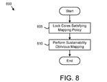
- FIG. 8 is a schematic flow chart diagram illustrating one embodiment of a sustainability-controlled mapping method 600 .
- the method 600 may perform the functions of the semiconductor 100 and the apparatus 400 , and in particular may perform sustainability controlled mapping.
- the method 600 may be performed using the processor 305 .
- the method 600 may be performed by a program product.
- the program product may comprise a computer readable storage medium, such as the memory 310 , storing program code.
- the processor 305 may execute the program code to perform the functions of the method 600 .
- the method 600 starts, and in one embodiment, the thread-to-core mapping module 240 locks 605 the cores 105 that satisfy the mapping policy 415 .
- the mapping policy 415 may be satisfied when the WAC 235 for a core 105 exceeds a specified WAC threshold.
- a process thread may not be assigned to a locked core 105 .
- the thread-to-core mapping module 240 may further perform the sustainability oblivious mapping of method 501 as described in FIG. 7 to map the scheduled process threads 272 the cores 105 and the method 600 ends.
- the thread-to-core mapping module 240 may further perform the sustainability oblivious mapping of method 501 as described in FIG. 7 to map the scheduled process threads 272 the cores 105 and the method 600 ends.
- FIG. 9 is a schematic flow chart diagram illustrating one embodiment of a sustainability-aware mapping method 601 .
- the method 601 may perform the functions of the semiconductor 100 and the apparatus 400 , and in particular may perform sustainability aware mapping.
- the method 601 may be performed using the processor 305 .
- the method 601 may be performed by a program product.
- the program product may comprise a computer readable storage medium, such as the memory 310 , storing program code.
- the processor 305 may execute the program code to perform the functions of the method 601 .
- the method 601 starts, and in one embodiment the thread-to-core mapping module 240 locks 615 cores 105 that satisfy the mapping policy 415 .
- the mapping policy 415 may be satisfied when the WAC 235 for a core 105 exceeds the specified WAC threshold.
- the thread-to-core mapping module 240 further selects 620 a first core 105 from the locked cores 105 and unlocks 625 the first core 105 .
- a process thread may be assigned to an unlocked core 105 .
- the thread-to-mapping module 240 determines 630 if the first core 105 is assigned to a process thread. If the first core 105 is not assigned, the thread-to-core mapping module 240 relocks 660 the first core 105 and selects 620 a new first core 105 .
- the thread-to-core mapping module 240 records 635 a first process thread assigned to the first core 105 and locks 640 the first core 105 .
- the thread-to-core mapping module 240 further performs 645 the sustainability oblivious mapping of the method 501 described in FIG. 7 .
- the thread-to-core mapping module 240 identifies 650 a second core 105 that is assigned to the first process thread and calculates 655 an energy delay for the first and second cores 105 .
- the energy delay edl is calculated for each core 105 using Equation 5, where e is an estimated energy for the core 105 , and d is a delay for the core 105 .
- edl e*d 2 Equation 5
- the thread-to-core mapping module 240 may further determine 665 if the mapping policy 415 is satisfied.
- the mapping policy 415 is satisfied in response to the expected energy efficiency for the first core 105 exceeding an efficiency threshold for the first core 105 , wherein the WAC 235 for the first core 105 also exceeds the WAC threshold.
- the mapping policy 415 may be satisfied if the utilization 285 for the first core 105 does not exceed the energy delay for the first core 105 .
- the mapping policy 415 is satisfied if the inequality of Equation 6 is satisfied, where edl is the energy delay, AW is a non-zero aging weight, util(l) is a utilization 285 of the locked first core 105 , and WAC(l) is the WAC 235 for the locked first core 105 , and l is the first locked core 105 .
- edl >AW*( util ( l ) ⁇ WAC( l )) Equation 6
- the thread-to-core mapping module 240 unlocks 670 the first core 105 and determines 675 if all cores 105 have been analyzed. If the error delay condition is not satisfied, the thread-to-core mapping module 240 determines 675 if all cores 105 have been analyzed.
- the thread-to-core mapping module 240 performs 680 the sustainability oblivious mapping of method 501 described in FIG. 7 and the method 601 ends. If all the cores 105 have not been analyzed, the thread-to-core mapping module 240 selects 620 a new and unanalyzed first core 105 from the locked cores and the method 601 continues.
- the embodiments may increase the energy efficiency, increase the sustainability, or increase both the sustainability and the energy efficiency for the cores 105 of the differentially reliable semiconductor 100 .
- the embodiments consistently delivered superior energy efficiency when compared with cores 105 mapped with an alternative race-to-idle algorithm.
- the energy efficiency for process threads mapped with the embodiments increases as more of the cores 105 within the semiconductor 100 are not powered.
Landscapes
- Engineering & Computer Science (AREA)
- Theoretical Computer Science (AREA)
- Physics & Mathematics (AREA)
- General Engineering & Computer Science (AREA)
- General Physics & Mathematics (AREA)
- Quality & Reliability (AREA)
- Software Systems (AREA)
- Power Sources (AREA)
Abstract
Description
er(t)=r(0)−r(t) Figure 1
ed(t)=d(t)−r(t) Equation 3
w(t)=(1−γ)1−K p ed(t) Equation 4
edl=e*d 2 Equation 5
edl>AW*(util(l)−WAC(l)) Equation 6
Claims (20)
Priority Applications (1)
| Application Number | Priority Date | Filing Date | Title |
|---|---|---|---|
| US14/046,335 US9213577B2 (en) | 2013-10-04 | 2013-10-04 | Sustainable differentially reliable architecture for dark silicon |
Applications Claiming Priority (1)
| Application Number | Priority Date | Filing Date | Title |
|---|---|---|---|
| US14/046,335 US9213577B2 (en) | 2013-10-04 | 2013-10-04 | Sustainable differentially reliable architecture for dark silicon |
Publications (2)
| Publication Number | Publication Date |
|---|---|
| US20150100930A1 US20150100930A1 (en) | 2015-04-09 |
| US9213577B2 true US9213577B2 (en) | 2015-12-15 |
Family
ID=52778011
Family Applications (1)
| Application Number | Title | Priority Date | Filing Date |
|---|---|---|---|
| US14/046,335 Expired - Fee Related US9213577B2 (en) | 2013-10-04 | 2013-10-04 | Sustainable differentially reliable architecture for dark silicon |
Country Status (1)
| Country | Link |
|---|---|
| US (1) | US9213577B2 (en) |
Cited By (1)
| Publication number | Priority date | Publication date | Assignee | Title |
|---|---|---|---|---|
| WO2018018492A1 (en) * | 2016-07-28 | 2018-02-01 | 张升泽 | Method and system of allocating current in plurality of intervals in interior of multi-core chip |
Families Citing this family (5)
| Publication number | Priority date | Publication date | Assignee | Title |
|---|---|---|---|---|
| US20180143853A1 (en) * | 2016-11-18 | 2018-05-24 | Qualcomm Incorporated | Circuits and Methods Providing Core Scheduling in Response to Aging for a Multi-Core Processor |
| US11256314B2 (en) | 2019-08-09 | 2022-02-22 | Dell Products L.P. | System and method for power management of field-programmable gate arrays and load balancing of personality bitstreams from a baseboard management controller |
| US11442885B2 (en) | 2019-08-09 | 2022-09-13 | Dell Products L.P. | System and method to change field-programmable gate array personality from a baseboard management controller |
| US10942766B2 (en) | 2019-08-09 | 2021-03-09 | Dell Products, L.P. | System and method for providing heterogeneous personality bitstreams on field-programmable gate arrays from a baseboard management controller |
| US12189467B2 (en) * | 2022-02-04 | 2025-01-07 | Hub data security Ltd. | Method to improve accuracy in fault tree analysis (FTA) |
Citations (2)
| Publication number | Priority date | Publication date | Assignee | Title |
|---|---|---|---|---|
| US20090307636A1 (en) * | 2008-06-05 | 2009-12-10 | International Business Machines Corporation | Solution efficiency of genetic algorithm applications |
| US8615724B2 (en) * | 2011-12-29 | 2013-12-24 | Flextronics Ap Llc | Circuit assembly yield prediction with respect to form factor |
-
2013
- 2013-10-04 US US14/046,335 patent/US9213577B2/en not_active Expired - Fee Related
Patent Citations (2)
| Publication number | Priority date | Publication date | Assignee | Title |
|---|---|---|---|---|
| US20090307636A1 (en) * | 2008-06-05 | 2009-12-10 | International Business Machines Corporation | Solution efficiency of genetic algorithm applications |
| US8615724B2 (en) * | 2011-12-29 | 2013-12-24 | Flextronics Ap Llc | Circuit assembly yield prediction with respect to form factor |
Non-Patent Citations (28)
| Title |
|---|
| Ancajas, D. M., et al., Proactive aging management in heterogeneous NoCs through a criticality-driven routing approach, Design, Automation & Test in Europe Conference & Exhibition, Mar. 18-22, 2013, p. 1032-1037. |
| Assayad, I., et al., Tradeoff exploration between reliability, power consumption, and execution time, Computer Safety, Reliability, and Security, 2011, p. 437-451. |
| Bhardwaj, S., et al., Predictive Modeling of the NBTI Effect for Reliable Design, Custom Integrated Circuits Conference, Sep. 10-13, 2006, p. 189-192. |
| Calimera, A., et al., NBTI-Aware Power Gating for Concurrent Leakage and Aging Optimization, Proceedings of the 14th ACM/IEEE international symposium on low power electronics and design, 2009, p. 127-132. |
| Chippa, V.K., et al., Analysis and Characterization of Inherent Application Resilience for Approximate Computing, Design Automation Conference, May 29-Jun. 29, 2013, p. 1-9. |
| Chong, I. S., et al., Hardware Testing for Error Tolerant Multimedia Compression based on Linear Transforms, Defects and Fault Tolerance in VLSI Systems, Oct. 3-5, 2005, p. 523-531. |
| Choudhary, V. K., et al., FabScalar: Composing Synthesizable RTL Designs of Arbitrary Cores within a Canonical Superscalar Template, Proceedings of the 38th Annual International Symposium on Computer Architecture, 2011, p. 11-22. |
| Chung, H., et al., Analysis and Testing for Error Tolerant Motion Estimation, Defect and Fault Tolerance in VLSI Systems, Oct. 3-5, 2005, p. 514-522. |
| Das, S., et al., Razorll: In Situ Error Detection and Correction for PVT and SER Tolerance, Solid-State Circuits, Jan. 2009, p. 32-48, vol. 44, iss. 1. |
| Dimitrov, M., et al., Understanding Software Approaches for GPGPU Reliability, GPGPU-2 Proceedings of 2nd Workshop on General Purpose Processing on Graphics Processing Units, 2009, p. 94-104. |
| Esmaeilzadeh, H., et al., Dark Silicon and the End of Multicore Scaling, ISCA '11 Proceedings of the 38th Annual International Symposium on Computer Architecture, 2011, p. 365-376. |
| Goulding-Hotta, N., et al., GreenDroid: An Architecture for the Dark Silicon Age, Design Automation Conference, Jan. 30-Feb. 2, 2012, p. 100-105. |
| Hardavellas, N., et al., Toward Dark Silicon in Servers, IEEE Micro, Jul./Aug. 2011, p. 6-15, vol. 31, iss. 4. |
| Kahng, A., et al., Designing a Processor From the Ground Up to Allow Voltage/Reliability Tradeoffs, High Performance Computer Architecture, Jan. 9-14, 2010, p. 1-11. |
| Leem, L., et al., ERSA: Error-Resilient System Architecture for Probabilistic Applications, Design, Automation & Test in Europe Conference & Exhibition, Mar. 8-12, 2010, p. 1560-1591. |
| Li, X., et al., Application-Level Correctness and its Impact on Fault Tolerance, High Performance Computer Architecture, Feb. 10-14, 2007, p. 181-192. |
| Lu, Y., et al., Statistical Reliability Analysis Under Process Variation and Aging Effects, Design Automation Conference, Jul. 26-31, 2009, p. 514-519. |
| Magnusson, P. S., et al., Simics: A Full System Simulation Platform, Computer, Feb. 2002, p. 50-58, vol. 35, iss. 2. |
| Nowroth, D., et al., A Study of Cognitive Resilience in a JPEG Compressor, Dependable Systems and Networks with FTCS and DCC, Jun. 24-27, 2008, p. 32-41. |
| Pop et al., Scheduling and Voltage Scaling for Energy/Reliability Trade-offs in Fault-Tolerant Time-Triggered Embedded Systems, ACM, Oct. 3, 2007, pp. 233-238. * |
| Pop, P., et al., Scheduling and Voltage Scaling for Energy/Reliability Trade-offs in Fault-Tolerant Time-Triggered Embedded Systems, Hardware/Software Codesign and System Synthesis, Sep. 30-Oct. 3, 2007, p. 233-238. |
| Sherwood, T., et al., Basic Block Distribution Analysis to Find Periodic Behavior and Simulation Points in Applications, Parallel Architectures and Compilation Techniques, 2001, p. 3-14. |
| Shim, B., et al., Energy-Efficient Soft Error-Tolerant Digital Signal Processing, Very Large Scale Integration (VLSI) Systems, Apr. 2006, p. 336-348, vol. 14, iss. 4. |
| Song, W., et al., Reliability Implications of Power / Thermal Constrained Operations in Asymmetric Multicore Processors, Proceedings of Dark Silicon (DaSi), 2012. |
| Srinivasan, J., et al., Exploiting Structural Duplication for Lifetime Reliability Enhancement, Computer Architecture, Jun. 4-8, 2005, p. 520-531. |
| Taylor, M. B., Is Dark Silicon Useful? Harnessing the Four Horsemen of the Coming Dark Silicon Apocalypse, Design Automation Conference, Jun. 3-7, 2012, p. 1131-1136. |
| Williams, D., et al., A Cross-Layer Approach to Heterogeneity and Reliability, Formal Methods and Models for Co-Design, Jul. 13-15, 2009, p. 88-97. |
| Zhang, Y., et al., Lighting the Dark Silicon by Exploiting Heterogeneity on Future Processors, Design Automation Conference, May 29-Jun. 7, 2013, p. 1-7. |
Cited By (1)
| Publication number | Priority date | Publication date | Assignee | Title |
|---|---|---|---|---|
| WO2018018492A1 (en) * | 2016-07-28 | 2018-02-01 | 张升泽 | Method and system of allocating current in plurality of intervals in interior of multi-core chip |
Also Published As
| Publication number | Publication date |
|---|---|
| US20150100930A1 (en) | 2015-04-09 |
Similar Documents
| Publication | Publication Date | Title |
|---|---|---|
| US9213577B2 (en) | Sustainable differentially reliable architecture for dark silicon | |
| CN104778074B (en) | A kind of calculating task processing method and processing device | |
| TWI361573B (en) | Symbol detector and sphere decoding method | |
| US20150248312A1 (en) | Performance-aware job scheduling under power constraints | |
| US20120215764A1 (en) | Energy usage and performance query governor | |
| CN106201722A (en) | The load regulation method of server and system | |
| US8712998B2 (en) | Deadline-driven parallel execution of queries | |
| CN113723593B (en) | A load-shedding prediction method and system based on neural network | |
| CN112801331B (en) | Shaping of computational loads with virtual capacity and preferred location real-time scheduling | |
| CN106844027A (en) | A kind of method for scheduling task based on node load | |
| CN110674569A (en) | Method and system for estimating remaining charging time based on decision tree | |
| US20150057975A1 (en) | Frequency guard band validation of processors | |
| TW201716920A (en) | Controlling voltage deviations in processing systems | |
| CN109831356A (en) | Data processing method, device, system, computer readable storage medium | |
| US9135563B2 (en) | Using cyclic Markov decision process to determine optimum policy | |
| US7607132B2 (en) | Process scheduling system and method | |
| US9997944B2 (en) | Method and system of charging a battery | |
| CN106570585B (en) | A task scheduling method and energy management device for a self-powered system | |
| WO2016197621A1 (en) | Method and apparatus for adjusting frequency of server | |
| US11404907B2 (en) | Distributed voltage control for power networks | |
| Wu et al. | An estimation of distribution algorithm to optimize the utility of task scheduling under fog computing systems | |
| CN116488242B (en) | Energy self-adaptive adjustment and digestion method and device in power interaction | |
| KR102145402B1 (en) | Method and apparatus for determining energy conservation measure for buliding retrofit | |
| WO2016082867A1 (en) | Orchestrator and method for virtual network embedding | |
| CN115016926B (en) | A resource-cost-based strategy selection method, system, electronic device, and storage medium |
Legal Events
| Date | Code | Title | Description |
|---|---|---|---|
| AS | Assignment |
Owner name: UTAH STATE UNIVERSITY, UTAH Free format text: ASSIGNMENT OF ASSIGNORS INTEREST;ASSIGNORS:ALLRED, JASON M;CHAKRABORTY, KOUSHIK;ROY, SANGHAMITRA;SIGNING DATES FROM 20131009 TO 20131107;REEL/FRAME:031668/0787 |
|
| STCF | Information on status: patent grant |
Free format text: PATENTED CASE |
|
| MAFP | Maintenance fee payment |
Free format text: PAYMENT OF MAINTENANCE FEE, 4TH YEAR, MICRO ENTITY (ORIGINAL EVENT CODE: M3551); ENTITY STATUS OF PATENT OWNER: MICROENTITY Year of fee payment: 4 |
|
| FEPP | Fee payment procedure |
Free format text: MAINTENANCE FEE REMINDER MAILED (ORIGINAL EVENT CODE: REM.); ENTITY STATUS OF PATENT OWNER: MICROENTITY |
|
| LAPS | Lapse for failure to pay maintenance fees |
Free format text: PATENT EXPIRED FOR FAILURE TO PAY MAINTENANCE FEES (ORIGINAL EVENT CODE: EXP.); ENTITY STATUS OF PATENT OWNER: MICROENTITY |
|
| STCH | Information on status: patent discontinuation |
Free format text: PATENT EXPIRED DUE TO NONPAYMENT OF MAINTENANCE FEES UNDER 37 CFR 1.362 |
|
| FP | Lapsed due to failure to pay maintenance fee |
Effective date: 20231215 |