US9203159B2 - Phased-array transceiver - Google Patents
Phased-array transceiver Download PDFInfo
- Publication number
- US9203159B2 US9203159B2 US13/371,924 US201213371924A US9203159B2 US 9203159 B2 US9203159 B2 US 9203159B2 US 201213371924 A US201213371924 A US 201213371924A US 9203159 B2 US9203159 B2 US 9203159B2
- Authority
- US
- United States
- Prior art keywords
- positions
- antenna
- selecting
- antenna positions
- arrangement
- Prior art date
- Legal status (The legal status is an assumption and is not a legal conclusion. Google has not performed a legal analysis and makes no representation as to the accuracy of the status listed.)
- Active, expires
Links
Images


Classifications
-
- H—ELECTRICITY
- H01—ELECTRIC ELEMENTS
- H01Q—ANTENNAS, i.e. RADIO AERIALS
- H01Q21/00—Antenna arrays or systems
- H01Q21/06—Arrays of individually energised antenna units similarly polarised and spaced apart
- H01Q21/061—Two dimensional planar arrays
-
- H—ELECTRICITY
- H01—ELECTRIC ELEMENTS
- H01Q—ANTENNAS, i.e. RADIO AERIALS
- H01Q21/00—Antenna arrays or systems
- H01Q21/06—Arrays of individually energised antenna units similarly polarised and spaced apart
- H01Q21/061—Two dimensional planar arrays
- H01Q21/065—Patch antenna array
-
- H—ELECTRICITY
- H01—ELECTRIC ELEMENTS
- H01L—SEMICONDUCTOR DEVICES NOT COVERED BY CLASS H10
- H01L23/00—Details of semiconductor or other solid state devices
- H01L23/58—Structural electrical arrangements for semiconductor devices not otherwise provided for, e.g. in combination with batteries
-
- H—ELECTRICITY
- H01—ELECTRIC ELEMENTS
- H01Q—ANTENNAS, i.e. RADIO AERIALS
- H01Q1/00—Details of, or arrangements associated with, antennas
- H01Q1/12—Supports; Mounting means
- H01Q1/22—Supports; Mounting means by structural association with other equipment or articles
-
- H—ELECTRICITY
- H01—ELECTRIC ELEMENTS
- H01Q—ANTENNAS, i.e. RADIO AERIALS
- H01Q23/00—Antennas with active circuits or circuit elements integrated within them or attached to them
-
- H—ELECTRICITY
- H04—ELECTRIC COMMUNICATION TECHNIQUE
- H04B—TRANSMISSION
- H04B7/00—Radio transmission systems, i.e. using radiation field
- H04B7/02—Diversity systems; Multi-antenna system, i.e. transmission or reception using multiple antennas
- H04B7/04—Diversity systems; Multi-antenna system, i.e. transmission or reception using multiple antennas using two or more spaced independent antennas
-
- H—ELECTRICITY
- H01—ELECTRIC ELEMENTS
- H01L—SEMICONDUCTOR DEVICES NOT COVERED BY CLASS H10
- H01L2224/00—Indexing scheme for arrangements for connecting or disconnecting semiconductor or solid-state bodies and methods related thereto as covered by H01L24/00
- H01L2224/01—Means for bonding being attached to, or being formed on, the surface to be connected, e.g. chip-to-package, die-attach, "first-level" interconnects; Manufacturing methods related thereto
- H01L2224/10—Bump connectors; Manufacturing methods related thereto
- H01L2224/15—Structure, shape, material or disposition of the bump connectors after the connecting process
- H01L2224/16—Structure, shape, material or disposition of the bump connectors after the connecting process of an individual bump connector
- H01L2224/161—Disposition
- H01L2224/16151—Disposition the bump connector connecting between a semiconductor or solid-state body and an item not being a semiconductor or solid-state body, e.g. chip-to-substrate, chip-to-passive
- H01L2224/16221—Disposition the bump connector connecting between a semiconductor or solid-state body and an item not being a semiconductor or solid-state body, e.g. chip-to-substrate, chip-to-passive the body and the item being stacked
- H01L2224/16225—Disposition the bump connector connecting between a semiconductor or solid-state body and an item not being a semiconductor or solid-state body, e.g. chip-to-substrate, chip-to-passive the body and the item being stacked the item being non-metallic, e.g. insulating substrate with or without metallisation
-
- Y—GENERAL TAGGING OF NEW TECHNOLOGICAL DEVELOPMENTS; GENERAL TAGGING OF CROSS-SECTIONAL TECHNOLOGIES SPANNING OVER SEVERAL SECTIONS OF THE IPC; TECHNICAL SUBJECTS COVERED BY FORMER USPC CROSS-REFERENCE ART COLLECTIONS [XRACs] AND DIGESTS
- Y10—TECHNICAL SUBJECTS COVERED BY FORMER USPC
- Y10T—TECHNICAL SUBJECTS COVERED BY FORMER US CLASSIFICATION
- Y10T29/00—Metal working
- Y10T29/49—Method of mechanical manufacture
- Y10T29/49002—Electrical device making
- Y10T29/49016—Antenna or wave energy "plumbing" making
Definitions
- the present invention relates to transceivers, and more particularly to phased-array transceiver systems, devices, apparatuses and methods of their packaging and fabrication.
- phased-array transceiver system packages are typically arranged in a uniform pattern.
- the uniform pattern assists in assuring that interference-inducing side lobes of radiation patterns are minimized.
- phased-antenna arrays can be formed in integrated circuit packages, and larger, scaled arrays can be formed by placing multiple packages adjacent to one another on a circuit board.
- An existing package for a transceiver device operating at 60 GHz employs 16 antennas that are distributed over a 28 ⁇ 28 mm 2 ball-grid array (BGA).
- One embodiment is directed to a method for fabricating an integrated circuit package containing antenna elements.
- a first set of antenna positions in a first section of a set of sections of a circuit layout for the circuit package is selected.
- the method further includes selecting another set of antenna positions in another section of the circuit layout such that an arrangement of selected antenna positions of the other set is different from an arrangement of selected antenna positions of a previously selected set of antenna positions.
- the selecting another set of positions in another section is iterated until selections have been made for a total number of antennas. Further, the selecting the other set is performed such that consecutive unselected positions in the other section do not exceed a predetermined number of positions.
- antenna elements are formed at the selected positions to fabricate the circuit package.
- the system includes a storage medium and a computation module.
- the storage medium is configured to store a circuit layout for the circuit package.
- the computation module is configured to select a first set of antenna positions in a first section of a set of sections of the circuit layout, select another set of antenna positions in another section of the circuit layout such that an arrangement of selected antenna positions of the other set is different from an arrangement of selected antenna positions of a previously selected set of antenna positions, and iterate the selection of another set of positions until selections have been made for a total number of antennas.
- the selection of the other set is performed such that consecutive unselected positions in any portion of the circuit layout do not exceed a predetermined number of positions.
- An alternative embodiment is directed to a computer readable storage medium including a computer readable program for forming a circuit package.
- the computer readable program when executed on a computer causes the computer to perform a plurality of steps.
- the steps include selecting a first set of a number (N) of antenna positions in a first section of a number (M) of sections of a circuit layout for the circuit package.
- each of the sections of the circuit layout is composed of M selectable antenna positions.
- the steps further include selecting another set of N antenna positions in another section of the M sections of the circuit layout such that an arrangement of selected antenna positions of the other set is different from an arrangement of selected antenna positions of a previously selected set of antenna positions.
- the steps also include iterating the selecting of another set of positions until selections have been made for a total number of antennas. The selection of the other set is performed such that consecutive unselected positions in any portion of the circuit layout do not exceed
- the circuit device includes integrated circuitry and a set of antenna elements.
- the integrated circuitry is configured to process communication signals.
- the set of antenna elements is coupled to the circuitry and is arranged on a circuit layout composed of a plurality of sections of positions. At least one section of the circuit layout is composed of an arrangement of antennas that is different from an arrangement of antennas of at least other section of the circuit layout. Further, consecutive unused positions in any of the sections do not exceed a predetermined number of positions.
- An alternative embodiment is directed to a transceiver apparatus that includes a plurality of integrated circuit packages.
- the circuit packages are assembled such that each given package of the packages is oriented differently from any packages that are adjacent to the given package.
- each of the packages includes a set of antenna elements and integrated circuitry.
- the set of antenna elements is arranged on a circuit board layout composed of a plurality of sections of positions. At least one section of the circuit layout is composed of an arrangement of antennas that is different from an arrangement of antennas of at least other section of the circuit layout. Here, consecutive unused positions in any of the sections do not exceed a predetermined number of positions.
- the integrated circuitry is coupled to the set of antenna elements and is configured to process at least one of: a) signals for transmission through antenna elements in the set of antenna elements or b) signals received through antenna elements in the set of antenna elements.
- FIG. 1 is a high-level block/flow diagram illustrating a view of a transceiver device in accordance with an exemplary embodiment of the present principles
- FIG. 2 is a high-level block/flow diagram illustrating another view of the transceiver device of FIG. 1 ;
- FIG. 3 is a high-level block diagram illustrating top view of circuit package in accordance with an exemplary aspect of the present principles
- FIG. 4 is a high-level block diagram illustrating bottom view of the circuit package of FIG. 3 ;
- FIG. 5 is a high-level block diagram of an antenna in accordance with an exemplary embodiment
- FIG. 6 is a high-level block diagram of a scaled antenna array comprised of circuit packages in accordance with an exemplary embodiment
- FIG. 7 is a diagram of a simulated radiation pattern of a scaled integrated circuit comprising circuit packages that utilize a random arrangement of antennas in accordance with an exemplary embodiment
- FIG. 8 is a diagram of a simulated radiation pattern of a scaled integrated circuit comprising circuit packages that utilize a uniform-pattern arrangement of antennas with a 100% fill factor;
- FIG. 9 is a high-level block diagram of the scaled integrated circuit for which the radiation pattern of FIG. 7 was simulated.
- FIG. 10 is a high-level block diagram of a scaled antenna array comprising integrated circuit packages that utilize a uniform-pattern arrangement of antennas;
- FIG. 11 is a diagram of a simulated radiation pattern of the scaled integrated circuit of FIG. 10 ;
- FIG. 12 is a high-level block/flow diagram of an exemplary method for fabricating a transceiver apparatus in accordance with an exemplary embodiment
- FIG. 13 is high-level diagram of a scaled antenna array comprising integrated circuit packages that utilize an alternative non-uniform arrangement of antennas in accordance with an exemplary embodiment
- FIG. 14 is a diagram of a simulated radiation pattern of the scaled integrated circuit of FIG. 13 ;
- FIG. 15 is a cross-sectional view of a circuit package in accordance with an exemplary embodiment
- FIG. 16 is high-level diagram of a scaled antenna array comprising integrated circuit packages that utilize an alternative non-uniform arrangement of antennas in accordance with an exemplary embodiment
- FIG. 17 is a high-level block diagram of a computer system that can implement features of exemplary embodiments.
- FIGS. 18 and 19 are diagrams of simulated co-polarization/cross-polarization radiation patterns on the E and H planes for horizontal and vertical ports, respectively, of an antenna element in accordance with an exemplary embodiment.
- transceiver packages can be constructed in a way that minimizes the size of interference-inducing side lobes of antenna array radiation patterns for the transceiver, while at the same time permitting simplified routing of connections between antenna elements and underlying integrated circuitry.
- the antenna elements of a circuit package can be arranged in a distinctly non-uniform manner to minimize the collective side lobes of radiation patterns of large scale arrays.
- sections of the circuit layout can include different arrangements of antenna elements.
- the antenna elements can be incorporated into the package such that a pre-determined spacing threshold between antenna is not exceeded. For example, assuming that an array of M ⁇ M of antenna locations are available in the package and there are N ⁇ N antenna elements that are to be incorporated into the package, the selections of antenna element locations can be made such that there are no more than
- the antenna array M 2 - N 2 M + 1 consecutive empty or dummy locations in the antenna array.
- this threshold also assists in scaling the packages, as it prevents the occurrence of large void regions between packages that are tiled to form a scaled circuit.
- the selections of antenna locations can be configured such that differences between selected arrangements of antenna in different areas of the package can be moderated to facilitate the routing of connections between integrated circuit elements and the antenna.
- aspects of the present invention may be embodied as a system, method, apparatus, device or computer program product. Accordingly, aspects of the present invention may take the form of an entirely hardware embodiment, an entirely software embodiment (including firmware, resident software, micro-code, etc.) or an embodiment combining software and hardware aspects that may generally be referred to herein as a “circuit,” “module” or “system.” Furthermore, aspects of the present invention may take the form of a computer program product embodied in one or more computer readable medium(s) having computer readable program code embodied thereon.
- the computer readable medium may be a computer readable signal medium or a computer readable storage medium.
- a computer readable storage medium may be, for example, but not limited to, an electronic, magnetic, optical, electromagnetic, infrared, or semiconductor system, apparatus, or device, or any suitable combination of the foregoing.
- a computer readable storage medium may be any tangible medium that can contain, or store a program for use by or in connection with an instruction execution system, apparatus, or device.
- a computer readable signal medium may include a propagated data signal with computer readable program code embodied therein, for example, in baseband or as part of a carrier wave. Such a propagated signal may take any of a variety of forms, including, but not limited to, electro-magnetic, optical, or any suitable combination thereof.
- a computer readable signal medium may be any computer readable medium that is not a computer readable storage medium and that can communicate, propagate, or transport a program for use by or in connection with an instruction execution system, apparatus, or device.
- Program code embodied on a computer readable medium may be transmitted using any appropriate medium, including but not limited to wireless, wireline, optical fiber cable, RF, etc., or any suitable combination of the foregoing.
- Computer program code for carrying out operations for aspects of the present invention may be written in any combination of one or more programming languages, including an object oriented programming language such as Java, Smalltalk, C++ or the like and conventional procedural programming languages, such as the “C” programming language or similar programming languages.
- the program code may execute entirely on the user's computer, partly on the user's computer, as a stand-alone software package, partly on the user's computer and partly on a remote computer or entirely on the remote computer or server.
- the remote computer may be connected to the user's computer through any type of network, including a local area network (LAN) or a wide area network (WAN), or the connection may be made to an external computer (for example, through the Internet using an Internet Service Provider).
- LAN local area network
- WAN wide area network
- Internet Service Provider an Internet Service Provider
- These computer program instructions may also be stored in a computer readable medium that can direct a computer, other programmable data processing apparatus, or other devices to function in a particular manner, such that the instructions stored in the computer readable medium produce an article of manufacture including instructions which implement the function/act specified in the flowchart and/or block diagram block or blocks.
- the computer program instructions may also be loaded onto a computer, other programmable data processing apparatus, or other devices to cause a series of operational steps to be performed on the computer, other programmable apparatus or other devices to produce a computer implemented process such that the instructions which execute on the computer or other programmable apparatus provide processes for implementing the functions/acts specified in the flowchart and/or block diagram block or blocks.
- the computer system 1700 can include a processor 1710 and a memory 1702 .
- the memory 1702 can include random-access memory (RAM) 1706 and read-only memory (ROM) 1708 .
- the memory 1702 can further include a computer readable storage medium 1704 .
- the computer readable storage medium 1704 can store a program of instructions that can be implemented by the processor 1710 .
- the processor 1710 implement a computation module 1712 that performs the instructions stored on the memory 1702 , which can include features of methods described herein.
- the computation module 1712 can embody and implement several aspects of the present principles in the design and/or fabrication of a circuit package and/or a scaled integrated circuit.
- the computer system 1700 can further include input/output (I/O) interface(s) 1714 , which can comprise, for example, physical ports or WiFi devices, that can couple to external devices for communication of data between the computer system 1700 and the devices.
- I/O input/output
- Such devices can include a display device 1716 , network devices 1720 , such as routers for connections to external networks, including local area networks (LANs) and the internet, and other external devices 1718 , such as a mouse and a keyboard.
- blocks in the flowchart or block diagrams may represent a module, segment, or portion of code, which comprises one or more executable instructions for implementing the specified logical function(s).
- the functions noted in the block may occur out of the order noted in the figures. For example, two blocks shown in succession may, in fact, be executed substantially concurrently, or the blocks may sometimes be executed in the reverse order, depending upon the functionality involved.
- a design for an integrated circuit chip may be created in a graphical computer programming language, and stored in a computer storage medium (such as a disk, tape, physical hard drive, or virtual hard drive such as in a storage access network). If the designer does not fabricate chips or the photolithographic masks used to fabricate chips, the designer may transmit the resulting design by physical means (e.g., by providing a copy of the storage medium storing the design) or electronically (e.g., through the Internet) to such entities, directly or indirectly.
- the stored design is then converted into the appropriate format (e.g., GDSH) for the fabrication of photolithographic masks, which typically include multiple copies of the chip design in question that are to be formed on a wafer.
- the photolithographic masks are utilized to define areas of the wafer (and/or the layers thereon) to be etched or otherwise processed.
- the resulting integrated circuit chips can be distributed by the fabricator in raw wafer form (that is, as a single wafer that has multiple unpackaged chips), as a bare die, or in a packaged form.
- the chip is mounted in a single chip package (such as a plastic carrier, with leads that are affixed to a motherboard or other higher level carrier) or in a multichip package (such as a ceramic carrier that has either or both surface interconnections or buried interconnections).
- the chip is then integrated with other chips, discrete circuit elements, and/or other signal processing devices as part of either (a) an intermediate product, such as a motherboard, or (b) an end product.
- the end product can be any product that includes integrated circuit chips, ranging from toys and other low-end applications to advanced computer products having a display, a keyboard or other input device, and a central processor.
- the system 100 can be implemented as a SiGe BiCMOS (Bipolar Junction-Complementary metal-oxide-semiconductor) W-band phased-array chipset with an in-package antenna array that is suitable for building larger scalable arrays at the board level by tiling packaged integrated circuits (ICs) adjacent to each other.
- SiGe BiCMOS Bipolar Junction-Complementary metal-oxide-semiconductor
- the design can make use of antenna-in-package technology and the preferred embodiment includes at least a 4 ⁇ 4 array with at least a portion of the array formed with ⁇ /2 element spacing at a 90-GHz center frequency and approximately ⁇ 6 GHz bandwidth.
- the antenna elements 102 in this embodiment have dual polarization and can be implemented using a 288-pin BGA package.
- the receiver (Rx) portion, 104 V and 104 H , of the transceiver integrated circuit (IC) 100 has 32 inputs 103 , 16 for each of the two polarizations, and two outputs, 108 V , if the intermediate frequency (IF) is vertical (V)-polarized, and 108 H , if the IF is horizontal (H)-polarized, so that it is capable of simultaneously receiving both orthogonal polarizations.
- the Rx portion 104 V and 104 H of the IC 100 consists of 32 Radio Frequency (RF) front-ends 109 , arranged in two groups of 16 elements, one for each antenna polarization. This architecture permits for simultaneous reception in both polarizations.
- the transmitter (Tx) portion 106 of the IC 100 will have 16 outputs 107 so that it is capable of transmitting in either polarization.
- the Rx portion, 104 V and 104 H , of the IC 100 is configured to perform RF-path phase-shifting and gain equalization, followed by RF power-combining and down-conversion to IF.
- the Rx portion, 104 V and 104 H includes a digital I/O module 121 for the control of register arrays and for beam control.
- a digital controller 110 can control a low noise amplifier (LNA) 112 and can control a phase shifter 114 to implement gain equalization and phase-shifting.
- each 16-element sub-array 104 V and 104 H includes an independent power combiner 116 and down-conversion mixer 122 .
- a 16:1 RF power combiner in each of the Rx arrays 104 V and 104 H can implement the power-combining function.
- a common frequency multiplier 118 can provide an off-chip local oscillator (LO) reference signal 120 to both arrays 104 V and 104 H and can employ a mixer 122 , in each of the Rx arrays 104 V and 104 H , to implement down-conversion of the input signal to an IF.
- the LO reference signal 120 is distributed at the board level, which would be multiplied to create an internal LO signal for the mixer 122 .
- a separate combiner IC 150 illustrated in FIG. 6 , combines IF signals from the Rx ICs outputs 108 V and 108 H and provides the board-level LO reference 120 .
- the Tx portion 106 of the ICs 100 receives IF signals 124 from a distributor IC (not shown), up-converts the signals to RF, performs RF power-distribution, implements RF-path phase-shifting and amplitude control and performs power amplification.
- the Tx portion 106 of the IC 100 is shown in FIG. 2 .
- Tx portion 106 cane alternatively transmit on each polarization.
- the Tx portion 106 includes a digital I/O module 125 for the control of register arrays and for beam control.
- the IC 106 includes a frequency multiplier 122 that receives the off-chip LO reference signal 120 and multiplies the signal.
- the up-conversion mixer 126 combines the multiplied signal with the IF signal 124 , which can be polarized in either the horizontal or the vertical direction, to up-convert the signal to RF.
- a 1:16 power distribution network 128 receives the up-converted signal and distributes the signal to 16 RF front ends 130 , each of which is controlled by respective digital control modules 132 .
- the front ends 130 each include a phase shifter 131 that implements RF-path phase shifting and an amplifier 133 that implements amplitude control.
- each of the 16 RF phase-shifting front-ends 130 two copies of the final power amplifiers (PA) stages 134 V and 134 H are included for power amplification in order to drive both polarization feed lines to the antennas 102 .
- PA power amplifier
- the phase-shifting RF front-ends in both the transmitter and receiver portions implement 5 to 7b digital control of phase and amplitude and include local memory arrays to facilitate beam steering operation and calibration in the overall array.
- the antennas 102 are each a dual-polarized aperture-coupled stacked patch antenna.
- FIG. 5 One possible structure of a dual-polarized antenna 102 is illustrated in FIG. 5 , which includes a port 502 for horizontal polarization and a port 504 for vertical polarization. Preliminary simulations indicate that the antenna 102 has at least 15% return loss bandwidth and port isolation that is better than 25 dB.
- FIGS. 18 and 19 show the simulated co-polarization/cross-polarization radiation patterns on the E and H planes for the horizontal and vertical ports, respectively. The antenna front to back ratio is greater than 17 dB.
- the proposed transceivers can be packaged in a way that minimizes side lobes of the array radiation patterns, thereby avoiding quality degradation of the communication signals.
- a package with antennas can be characterized as having a size equivalent to a grid or matrix of M ⁇ M points. The spacing between the points in the grid is approximately ⁇ /2, where ⁇ is the wavelength of interest for the antenna array, as indicated above.
- the package houses a set of ICs that together feed or are coupled to a set of N ⁇ N antennae where N ⁇ M. Out of the M ⁇ M possible antenna locations in the package, only N ⁇ N locations are occupied.
- the packages are to be tiled in both x and y dimensions, forming a large-scale array. Exemplary embodiments can choose the antenna locations in the individual packages to minimize the sidelobes of the radiation pattern from the array while accounting for practical limitations of routing between the ICs and the package at mm-Wave frequencies.
- FIG. 3 illustrates a top view of one possible transceiver package 300 .
- the arrangement of antenna elements 102 in FIG. 3 is merely an example; other arrangements of antenna elements 102 can be implemented in the package 300 .
- the transceiver package 300 connects the phased-array ICs 100 , which are beneath the areas of the package denoted by lines 302 in FIG. 3 , to antennas 102 using flip-chip technology.
- the W-band input and outputs are routed to the antennas through vias 304 and 50- ⁇ interconnects 306 on the package 300 , while the direct current (DC) and analog connections 308 are routed to a ball-grid array.
- Multiple packages 300 can be attached to a printed circuit board, thereby enabling a tiled large-element array 600 , as illustrated in FIG. 6 , where each of the elements 602 can be implemented as package 300 .
- FIG. 3 one embodiment of the present principles is directed to a four-chip 100 package that incorporates 64 antennas 102 , 16 for each IC 100 , in a fractal pattern.
- FIG. 4 provides a bottom view of the package 300 , where elements 402 denote the portions of the BGA employed from DC and baseband connections. Sharing the DC and digital interconnects 308 and 306 among the four ICs 100 enables all four IC 100 to fit in a 16 ⁇ 16 mm 2 package, resulting in an array fill factor of 64%. This fill factor will be maintained for arbitrarily large arrays if the packages were combined, as illustrated in FIG. 6 .
- FIG. 4 provides a bottom view of the package 300 , where elements 402 denote the portions of the BGA employed from DC and baseband connections. Sharing the DC and digital interconnects 308 and 306 among the four ICs 100 enables all four IC 100 to fit in a 16 ⁇ 16 mm 2 package, resulting in an array fill factor of 64%. This fill factor will be maintained for
- FIG. 6 depicts a method of tiling multiple packages 602 (sub-arrays), which can be implemented with packages 300 , in a way that provides a contiguous ground plane across different packages.
- packages 602 with, for example, 64 antennas, can be tiled on a two-dimensional grid.
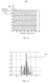
- FIG. 7 shows a simulated array pattern 700 for 4 ⁇ 4 tiles of a 10 ⁇ 10 array on 16 ⁇ 16 mm 2 packages (1600 antennas in total) that employ the fractal pattern of antennas of FIG. 3 .
- FIG. 8 shows a simulated array pattern 800 for 4 ⁇ 4 tiles of a 64 element array on 16 ⁇ 16 mm 2 packages (1024 antennas in total).
- FIG. 9 illustrates the 16 ⁇ 16 mm 2 packages that employ the fractal pattern of antennas of FIG. 3 .
- Both patterns 700 and 800 have an antenna beam width of 1.2°.
- the non-uniform array results in additional sidelobes that are not present in the uniform array.
- the peak sidelobe levels in the 64 element array are ⁇ 20 dB compared to the ⁇ 21 dB for the 100 element array, and the additional sidelobes are in the range of ⁇ 25 dB or less. It should be noted that no amplitude tapering or digital corrections are applied to the arrays, both of which can be used to significantly improve the sidelobe performance.
- Real planar arrays tend to show sidelobe levels in the ⁇ 10 to ⁇ 15 dB range without sidelobe level suppression. Coupling between antennas is a large factor in this behavior. This makes the simulated sidelobe level difference between the non-uniform and uniform arrays less significant in practice.
- FIGS. 3 , 6 and 9 provide benefits in terms of reducing side lobes of array radiation patterns, such arrangements may be relatively difficult to implement in the context of designing mm-Wave packages that house multiple ICs. For example, in this case, the routing from the ICs to each antenna would have to be customized. In addition, routing to particular locations may not be possible or may result in excessive losses, coupling or phase shift.
- FIG. 10 An arrangement 1000 of antenna 102 resulting from placing the N ⁇ N antennas together or in identical sub-groups is shown in FIG. 10 .
- this simple antenna placement strategy leads to systematic spacing 1002 , 1004 between antenna elements 102 .
- This deterministic placement might result in some values for the x and y array dimension variables being sampled many times while some values are not sampled at all.
- such a placement strategy produces systematic or periodic regions without antennas. Such regions in the arrangement result in large and systematic side lobes, as shown in FIG. 11 , illustrating the array radiation pattern 1100 for the arrangement 1000 .
- FIG. 12 illustratively depicts a method 1210 for designing and fabricating a circuit package in accordance with an exemplary embodiment.
- the method 1210 can be incorporated into a method 1200 for fabricating a transceiver apparatus by combining it with an assembly method 1230 .
- the methods 1210 and 1230 can be performed independently.
- at least a portion of the method 1200 can be performed by a processor of a computer system, such as the processor 1710 of the system 1700 of FIG. 17 .
- the computation module 1712 implemented by the processor 1710 can apply one or more portions of the method 1210 and/or the method 1230 to a circuit layout stored in the storage medium 1704 .
- the circuit layout can, for example, model the M ⁇ M possible antenna locations of the package 300 .
- the computation module 1712 can implement a program of instructions comprising steps of the method 1210 and/or the method 1230 .
- the method 1210 can begin at step 1212 , at which the computation module 1712 can select a first set of antenna positions in a first section of a set or plurality of sections of the circuit layout for the circuit package.
- the selection can be made such that consecutive unselected positions in the section does not exceed a pre-determined number K.
- the set or plurality of sections can represent the stacked rows of the M ⁇ M matrix of possible antenna locations of the package 300 .
- the computation module 1712 can be configured to select N antenna positions from the possible or selectable antenna positions in a row of the M ⁇ M matrix, where N ⁇ N is the total number of antenna that is to be formed in the package.
- the row can have up to
- K M 2 - N 2 M + 1 empty positions. It should be noted that the “first row” described here need not be the first row of the M ⁇ M matrix.
- the computation module 1712 select another set of antenna positions in another section of the circuit layout such that an arrangement of selected antenna positions of the other set is different from an arrangement of selected antenna positions of a previously selected set of antenna positions.
- the selection of the arrangement of antenna positions for the other section can be made such that at least one position in the arrangement is different from the arrangement of a previously selected set of antenna positions.
- the other section can, for example, be any other row of the M ⁇ M matrix, including a row that is above the first section or a row that is below the first section.
- the other row can be an adjacent row.
- the computation module 1712 can be configured to select N antenna positions from the other section.
- the method 1210 can then proceed to step 1216 , at which the computation module 1712 can determine whether selections have been made for a total number of antenna positions.
- the computation module 1712 can determine whether the antenna position selections for all N ⁇ N antenna to be included in the package have been made. If not, then the method can proceed to step 1214 and can be repeated. If selections have been made for the total number of antenna positions, then the method can proceed to step 1218 , at which the computation module 1712 can output the circuit layout that includes the selected antenna positions.
- the computation module 1712 can be configured to make the selections in steps 1212 and 1214 such that consecutive unselected positions in a section do not exceed a predetermined number (K) of positions.
- the computation module 1712 can perform the iterations of the step 1214 by making changes in the antenna locations from one row to the next in such a way as to avoid more than
- computation module 1712 can perform the steps 1214 and 1214 such that consecutive unselected positions do not exceed the
- the computation module 1712 can perform the steps 1214 and 1214 such that consecutive unselected positions do not exceed the predetermined number of K positions in any portion of the circuit layout.
- the computation module 1712 can perform the selections of steps 1212 and 1214 for rows of the M ⁇ M matrix in order in a vertical direction, where one or more rows can be skipped in the performance of any of steps 1212 and 1214 .
- the computation module 1712 can preferably perform the selections such that the “previously selected set of antenna positions” described above with respect to step 1214 is the set of antenna positions selected in an immediately preceding selection step.
- the difference in the arrangement of selected antenna positions is made with respect to the arrangement of the set of antenna positions selected in the immediately preceding selection step.
- the computation module 1712 preferably selects the arrangement of selected antenna positions such that the selected arrangement is unique with respect to as many previously selected arrangements as possible.
- the computation module 1712 preferably selects the arrangement of antenna positions such that the selected arrangement of selected antenna positions in an iteration of step 1214 is differed as little as possible from the arrangement of antenna positions selected in an immediately preceding selection step.
- the computation module 1712 is configured to change only one antenna location with respect to a set of antenna locations selected in an immediately preceding selection step such that the arrangement is unique with regard to the set of antenna locations selected in an immediately preceding selection step, if possible to meet the constraint that consecutive unselected positions are not exceeded in a section of the circuit layout, in the x and y directions of the circuit layout (i.e., if the matrix implementation is employed, in any row or column) and/or any portion of the circuit layout, depending on the constraint regarding consecutive unselected positions utilized.
- antenna elements can be formed in the positions of the circuit layout selected at steps 1212 and 1214 , as described above.
- the antenna elements can be formed in the positions of the circuit layout to form a package 300 , where an arrangement of antennas selected in accordance with the method 1200 can be formed to generate the package 300 .
- a particular example of the arrangement is illustrated in FIG. 13 , which is described in more detail herein below.
- unselected positions can correspond to positions that are empty or positions that are filled with dummy antenna, where the formation step 1220 can comprise activating or coupling the IC circuitry 100 to only selected antenna elements.
- the computation module 1712 can direct a physical, automated formation of the antenna elements 102 onto a circuit layout.
- the fabrication of the circuit package can be completed.
- the antenna elements 102 can be coupled to integrated circuits 100 to form the package 300 , as described above.
- the computation module 1712 can direct a physical, automated fabrication of the package 300 at step 1222 .
- the method 1200 can proceed to the package assembly method 1230 .
- the method 1230 can assemble multiple packages 300 generated in accordance with the method 1210 and the method 1230 can be performed by a production entity that is different from a production entity that implements the method 1210 .
- the methods 1210 and 1230 can be performed independently.
- the steps 1212 - 1218 can also form an independent method for embodiments directed to designing a circuit layout.
- the method 1230 can begin at step 1232 , at which circuit packages fabricated in accordance with the method 1210 can be received.
- the received circuit packages can be arranged and assembled.
- the computation module 1712 can direct the implementation of step 1234 .
- An exemplary arrangement 1300 of packages 300 that can be implemented in accordance with step 1234 is illustrated in FIG. 13 .
- each of the packages 300 can include an arrangement 1302 of antenna elements 102 , which can be formed in accordance with step 1220 .
- sixteen packages 300 (4 ⁇ 4 packages) are assembled to form the scaled IC 1300 .
- the corresponding simulated array radiation pattern 1400 for IC 1300 is shown in FIG. 14 . This array pattern has very similar side lobe levels as those attained by the ideal solution in FIG. 3 .
- the packages 300 can be arranged and assembled such that each given package of the received circuit packages is oriented differently from any packages that are adjacent to the given package.
- the packages 300 are tiled with a non-uniform orientation.
- adjacent packages can be rotated by 90 degrees with respect to one another.
- An example of this arrangement 1600 is illustrated in FIG. 16 , where each given package 300 is rotated by 90 degrees with respect to any packages that are adjacent to the given package.
- step 1236 the fabrication of the transceiver apparatus can be completed.
- the packages 300 can be fabricated by multiple sub-laminations, as illustrated in FIG. 15 .
- the package 300 can include a sub-laminate 1502 on which antenna elements 102 can be formed in the fractal pattern illustrated in FIG. 3 or in the non-uniform pattern 1302 of FIG. 13 .
- the package can also include a sub-laminate 1504 .
- Edge plating can be performed for some of the sub-laminates. Additionally, edge-plating can be used to form edges 1506 that are connected to the antenna ground 1504 . Further, plated edges can be directly soldered to each other to form a eutectic solder 1507 during or after BGA 1508 assembly on a board 1510 .
- the embodiments described herein above enable the fabrication of circuit packages that have negligible interference-inducing side lobes of antenna array radiation patterns. Furthermore, the arrangements of antenna elements described herein also permit simplified routing of connections between antenna elements and underlying integrated circuitry.
Abstract
Description
positions.
consecutive empty or dummy locations in the antenna array. In this way, for example, large empty or dummy regions of the antenna array, which contribute to side lobes of the array radiation pattern, can be avoided. Furthermore, use of this threshold also assists in scaling the packages, as it prevents the occurrence of large void regions between packages that are tiled to form a scaled circuit. In addition, the selections of antenna locations can be configured such that differences between selected arrangements of antenna in different areas of the package can be moderated to facilitate the routing of connections between integrated circuit elements and the antenna.
empty positions. It should be noted that the “first row” described here need not be the first row of the M×M matrix.
consecutive spaces (empty or unused locations) in either the x or y directions. Thus,
positions in any row or column of the matrix. Indeed, the
antenna locations appear between one package and the other. As noted above, large systematic spaces between antennas leads to large side-lobes. To avoid having these voids in a periodic fashion, at
Claims (16)
Priority Applications (8)
| Application Number | Priority Date | Filing Date | Title |
|---|---|---|---|
| US13/371,924 US9203159B2 (en) | 2011-09-16 | 2012-02-13 | Phased-array transceiver |
| PCT/IB2012/053142 WO2013038276A1 (en) | 2011-09-16 | 2012-06-21 | Phased-array transceiver |
| JP2014529091A JP5858550B2 (en) | 2011-09-16 | 2012-06-21 | Method for manufacturing a circuit package, system for forming a circuit package, computer readable storage medium including a computer readable program for forming a circuit package, circuit device and transceiver apparatus (phased array transceiver) |
| DE112012003358.2T DE112012003358T5 (en) | 2011-09-16 | 2012-06-21 | Phased array transceiver |
| CN201280044783.2A CN103797640B (en) | 2011-09-16 | 2012-06-21 | Phase array transceiver |
| GB1403466.4A GB2509414A (en) | 2011-09-16 | 2012-06-21 | Phased-array transceiver |
| US14/725,161 US9537224B2 (en) | 2011-09-16 | 2015-05-29 | Phased-array transceiver |
| JP2015190915A JP6176635B2 (en) | 2011-09-16 | 2015-09-29 | Method for manufacturing a circuit package, system for forming a circuit package, computer readable storage medium including a computer readable program for forming a circuit package, circuit device and transceiver apparatus (phased array transceiver) |
Applications Claiming Priority (2)
| Application Number | Priority Date | Filing Date | Title |
|---|---|---|---|
| US201161535759P | 2011-09-16 | 2011-09-16 | |
| US13/371,924 US9203159B2 (en) | 2011-09-16 | 2012-02-13 | Phased-array transceiver |
Related Child Applications (1)
| Application Number | Title | Priority Date | Filing Date |
|---|---|---|---|
| US14/725,161 Division US9537224B2 (en) | 2011-09-16 | 2015-05-29 | Phased-array transceiver |
Publications (2)
| Publication Number | Publication Date |
|---|---|
| US20130069831A1 US20130069831A1 (en) | 2013-03-21 |
| US9203159B2 true US9203159B2 (en) | 2015-12-01 |
Family
ID=47880174
Family Applications (2)
| Application Number | Title | Priority Date | Filing Date |
|---|---|---|---|
| US13/371,924 Active 2034-03-13 US9203159B2 (en) | 2011-09-16 | 2012-02-13 | Phased-array transceiver |
| US14/725,161 Active 2032-02-23 US9537224B2 (en) | 2011-09-16 | 2015-05-29 | Phased-array transceiver |
Family Applications After (1)
| Application Number | Title | Priority Date | Filing Date |
|---|---|---|---|
| US14/725,161 Active 2032-02-23 US9537224B2 (en) | 2011-09-16 | 2015-05-29 | Phased-array transceiver |
Country Status (6)
| Country | Link |
|---|---|
| US (2) | US9203159B2 (en) |
| JP (2) | JP5858550B2 (en) |
| CN (1) | CN103797640B (en) |
| DE (1) | DE112012003358T5 (en) |
| GB (1) | GB2509414A (en) |
| WO (1) | WO2013038276A1 (en) |
Cited By (6)
| Publication number | Priority date | Publication date | Assignee | Title |
|---|---|---|---|---|
| US9537224B2 (en) | 2011-09-16 | 2017-01-03 | International Business Machines Corporation | Phased-array transceiver |
| US20170033462A1 (en) * | 2015-07-28 | 2017-02-02 | Commissariat à l'Energie Atomique et aux Energies Alternatives | Transmitarray unit cell for a reconfigurable antenna |
| US20200021025A1 (en) * | 2018-07-16 | 2020-01-16 | Apple Inc. | Electronic Devices Having Distributed Millimeter Wave Antennas |
| US10784563B2 (en) | 2018-02-21 | 2020-09-22 | International Business Machines Corporation | Scalable phased array package |
| US10826194B2 (en) | 2018-02-21 | 2020-11-03 | International Business Machines Corporation | Scalable phased array package |
| US11189905B2 (en) | 2018-04-13 | 2021-11-30 | International Business Machines Corporation | Integrated antenna array packaging structures and methods |
Families Citing this family (23)
| Publication number | Priority date | Publication date | Assignee | Title |
|---|---|---|---|---|
| US9191057B2 (en) | 2012-12-28 | 2015-11-17 | International Business Machines Corporation | Scalable polarimetric phased array transceiver |
| US10756445B2 (en) * | 2014-12-12 | 2020-08-25 | The Boeing Company | Switchable transmit and receive phased array antenna with high power and compact size |
| US9882398B2 (en) * | 2015-01-05 | 2018-01-30 | Ossia Inc. | Techniques for reducing human exposure to wireless energy in wireless power delivery environments |
| US9905921B2 (en) | 2015-03-05 | 2018-02-27 | Kymeta Corporation | Antenna element placement for a cylindrical feed antenna |
| US9887455B2 (en) * | 2015-03-05 | 2018-02-06 | Kymeta Corporation | Aperture segmentation of a cylindrical feed antenna |
| EP3381085A4 (en) * | 2015-09-18 | 2019-09-04 | Anokiwave, Inc. | Laminar phased array |
| US10074900B2 (en) * | 2016-02-08 | 2018-09-11 | The Boeing Company | Scalable planar packaging architecture for actively scanned phased array antenna system |
| US9948407B2 (en) * | 2016-05-27 | 2018-04-17 | Huawei Technologies Co., Ltd. | Method and apparatus for beamforming calibration in point to multipoint communication systems |
| US9923712B2 (en) | 2016-08-01 | 2018-03-20 | Movandi Corporation | Wireless receiver with axial ratio and cross-polarization calibration |
| US10291296B2 (en) | 2016-09-02 | 2019-05-14 | Movandi Corporation | Transceiver for multi-beam and relay with 5G application |
| US10199717B2 (en) | 2016-11-18 | 2019-02-05 | Movandi Corporation | Phased array antenna panel having reduced passive loss of received signals |
| US9985733B1 (en) * | 2016-11-22 | 2018-05-29 | Keysight Technologies, Inc. | System and method for performing over-the-air (OTA) testing of a device under test (DUT) having an integrated transmitter-antenna assembly |
| DE102017200273A1 (en) * | 2017-01-10 | 2018-07-12 | Audi Ag | Radar arrangement for a motor vehicle and motor vehicle |
| US10484078B2 (en) | 2017-07-11 | 2019-11-19 | Movandi Corporation | Reconfigurable and modular active repeater device |
| US10063303B1 (en) * | 2017-09-18 | 2018-08-28 | Integrated Device Technology, Inc. | Fast memory access control for phase and gain |
| CN110098492B (en) * | 2018-01-27 | 2020-07-24 | 成都华为技术有限公司 | Dual-polarized antenna, radio frequency front-end device and communication equipment |
| EP3776872A2 (en) * | 2018-04-10 | 2021-02-17 | Starry, Inc. | Star topology fixed wireless access network with lower frequency failover |
| DE102019107258A1 (en) | 2018-05-24 | 2019-11-28 | Samsung Electronics Co., Ltd. | PHASED ARRAY ANTENNA MODULE AND COMMUNICATION DEVICE WITH THE SAME |
| KR102514744B1 (en) | 2018-07-30 | 2023-03-29 | 이노페이즈 인크. | System and method for massive MIMO communication |
| WO2020093005A1 (en) * | 2018-11-01 | 2020-05-07 | Innophase, Inc. | Reconfigurable phase array |
| KR102533885B1 (en) * | 2019-05-31 | 2023-05-18 | 가부시키가이샤 무라타 세이사쿠쇼 | Sub-array antenna, array antenna, antenna module and communication device |
| WO2022093996A1 (en) * | 2020-10-27 | 2022-05-05 | Mixcomm, Inc. | Methods and apparatus for implementing antenna assemblies and/or combining antenna assemblies to form arrays |
| US11710902B2 (en) | 2021-02-09 | 2023-07-25 | International Business Machines Corporation | Dual-polarized magneto-electric antenna array |
Citations (7)
| Publication number | Priority date | Publication date | Assignee | Title |
|---|---|---|---|---|
| US20060076658A1 (en) | 2004-10-13 | 2006-04-13 | Advanced Semiconductor Engineering, Inc. | Semiconductor package structure with microstrip antennan |
| CN1848430A (en) | 2005-04-15 | 2006-10-18 | 诠欣股份有限公司 | System chip capable of integrating micro-antenna |
| JP2007174443A (en) | 2005-12-23 | 2007-07-05 | Mitsubishi Electric Corp | Receiver equipment |
| US20090153158A1 (en) * | 2007-12-18 | 2009-06-18 | Sibeam, Inc. | Rf integrated circuit test methodology and system |
| US20100190464A1 (en) | 2009-01-27 | 2010-07-29 | International Business Machines Corporation | Simple radio frequency integrated circuit (rfic) packages with integrated antennas |
| US20100193935A1 (en) | 2009-01-30 | 2010-08-05 | Infineon Technologies Ag | Integrated antennas in wafer level package |
| JP2010219588A (en) | 2009-03-13 | 2010-09-30 | Japan Radio Co Ltd | Array antenna |
Family Cites Families (7)
| Publication number | Priority date | Publication date | Assignee | Title |
|---|---|---|---|---|
| US4771294A (en) * | 1986-09-10 | 1988-09-13 | Harris Corporation | Modular interface for monolithic millimeter wave antenna array |
| JP3907869B2 (en) * | 1999-07-02 | 2007-04-18 | 三菱電機株式会社 | Array antenna element thinning method and recording medium recording array antenna element thinning program |
| JP2006279604A (en) * | 2005-03-29 | 2006-10-12 | Tdk Corp | Surface acoustic wave device |
| JP2009171022A (en) * | 2008-01-11 | 2009-07-30 | Japan Aerospace Exploration Agency | Phased array antenna |
| US7696930B2 (en) * | 2008-04-14 | 2010-04-13 | International Business Machines Corporation | Radio frequency (RF) integrated circuit (IC) packages with integrated aperture-coupled patch antenna(s) in ring and/or offset cavities |
| TWI536661B (en) * | 2009-04-13 | 2016-06-01 | 凡爾賽特公司 | System for communication and method for communicating rf signals |
| US9203159B2 (en) | 2011-09-16 | 2015-12-01 | International Business Machines Corporation | Phased-array transceiver |
-
2012
- 2012-02-13 US US13/371,924 patent/US9203159B2/en active Active
- 2012-06-21 CN CN201280044783.2A patent/CN103797640B/en active Active
- 2012-06-21 DE DE112012003358.2T patent/DE112012003358T5/en active Pending
- 2012-06-21 GB GB1403466.4A patent/GB2509414A/en not_active Withdrawn
- 2012-06-21 WO PCT/IB2012/053142 patent/WO2013038276A1/en active Application Filing
- 2012-06-21 JP JP2014529091A patent/JP5858550B2/en active Active
-
2015
- 2015-05-29 US US14/725,161 patent/US9537224B2/en active Active
- 2015-09-29 JP JP2015190915A patent/JP6176635B2/en active Active
Patent Citations (7)
| Publication number | Priority date | Publication date | Assignee | Title |
|---|---|---|---|---|
| US20060076658A1 (en) | 2004-10-13 | 2006-04-13 | Advanced Semiconductor Engineering, Inc. | Semiconductor package structure with microstrip antennan |
| CN1848430A (en) | 2005-04-15 | 2006-10-18 | 诠欣股份有限公司 | System chip capable of integrating micro-antenna |
| JP2007174443A (en) | 2005-12-23 | 2007-07-05 | Mitsubishi Electric Corp | Receiver equipment |
| US20090153158A1 (en) * | 2007-12-18 | 2009-06-18 | Sibeam, Inc. | Rf integrated circuit test methodology and system |
| US20100190464A1 (en) | 2009-01-27 | 2010-07-29 | International Business Machines Corporation | Simple radio frequency integrated circuit (rfic) packages with integrated antennas |
| US20100193935A1 (en) | 2009-01-30 | 2010-08-05 | Infineon Technologies Ag | Integrated antennas in wafer level package |
| JP2010219588A (en) | 2009-03-13 | 2010-09-30 | Japan Radio Co Ltd | Array antenna |
Non-Patent Citations (3)
| Title |
|---|
| Haupt, R. "Thinned Arrays Using Genetic Algorithms" IEEE Transactions on Antennas and Propagation, vol. 42, No. 7. Jul. 1994. pp. 993-999. |
| International Search Report and Written Opinion for International Application No. PCT/IB2012/053142. Nov. 15, 2012. (10 Pages). |
| Kam, D., et al. "Organic Packages With Embedded Phased-Array Antennas for 60-Ghz Wireless Chipsets" IEEE Transactions on Components, Packaging and Manufacturing Technology, vol. 1, No. 11. Nov. 2011. pp. 1806-1814. |
Cited By (8)
| Publication number | Priority date | Publication date | Assignee | Title |
|---|---|---|---|---|
| US9537224B2 (en) | 2011-09-16 | 2017-01-03 | International Business Machines Corporation | Phased-array transceiver |
| US20170033462A1 (en) * | 2015-07-28 | 2017-02-02 | Commissariat à l'Energie Atomique et aux Energies Alternatives | Transmitarray unit cell for a reconfigurable antenna |
| US9941592B2 (en) * | 2015-07-28 | 2018-04-10 | Commissariat à l'Energie Atomique et aux Energies Alternatives | Transmitarray unit cell for a reconfigurable antenna |
| US10784563B2 (en) | 2018-02-21 | 2020-09-22 | International Business Machines Corporation | Scalable phased array package |
| US10826194B2 (en) | 2018-02-21 | 2020-11-03 | International Business Machines Corporation | Scalable phased array package |
| US11189905B2 (en) | 2018-04-13 | 2021-11-30 | International Business Machines Corporation | Integrated antenna array packaging structures and methods |
| US20200021025A1 (en) * | 2018-07-16 | 2020-01-16 | Apple Inc. | Electronic Devices Having Distributed Millimeter Wave Antennas |
| US11108155B2 (en) * | 2018-07-16 | 2021-08-31 | Apple Inc. | Electronic devices having distributed millimeter wave antennas |
Also Published As
| Publication number | Publication date |
|---|---|
| US9537224B2 (en) | 2017-01-03 |
| JP2016048915A (en) | 2016-04-07 |
| JP5858550B2 (en) | 2016-02-10 |
| CN103797640A (en) | 2014-05-14 |
| GB201403466D0 (en) | 2014-04-16 |
| JP6176635B2 (en) | 2017-08-09 |
| US20150288077A1 (en) | 2015-10-08 |
| US20130069831A1 (en) | 2013-03-21 |
| JP2014531801A (en) | 2014-11-27 |
| GB2509414A (en) | 2014-07-02 |
| DE112012003358T5 (en) | 2014-04-30 |
| CN103797640B (en) | 2015-09-09 |
| WO2013038276A1 (en) | 2013-03-21 |
Similar Documents
| Publication | Publication Date | Title |
|---|---|---|
| US9537224B2 (en) | Phased-array transceiver | |
| Ala-Laurinaho et al. | 2-D beam-steerable integrated lens antenna system for 5G $ E $-band access and backhaul | |
| CN108432088B (en) | Phased array antenna with sub-arrays | |
| US9397740B2 (en) | Modular antenna array with RF and baseband beamforming | |
| Gu et al. | A compact 4-chip package with 64 embedded dual-polarization antennas for W-band phased-array transceivers | |
| Guo et al. | Advanced antenna array engineering for 6G and beyond wireless communications | |
| Rupakula et al. | Limited scan-angle phased arrays using randomly grouped subarrays and reduced number of phase shifters | |
| SE511911C2 (en) | Antenna unit with a multi-layer structure | |
| EP2237373A1 (en) | Sub-array polarization control using rotated dual polarized radiating elements | |
| US20070063898A1 (en) | Phased array antenna with subarray lattices forming substantially rectangular aperture | |
| Kumar et al. | Dual circularly polarized spherical phased-array antenna for spacecraft application | |
| CN113451764A (en) | Multi-order sequentially-rotating circularly polarized antenna array | |
| Laue et al. | A checkered network for implementing arbitrary overlapped feed networks | |
| Vaccaro et al. | Low cost phased array for mobile Ku-band satellite terminal | |
| Moghaddam | Design of a compact multilayer circularly polarized phased array transmit antenna system for satellite applications | |
| Otto et al. | Planar Satcom antenna systems in Ka-band | |
| Cantrell et al. | Wideband array antenna concept | |
| US11502418B2 (en) | Network for forming multiple beams from a planar array | |
| WO2022061937A1 (en) | Antenna array, apparatus, and wireless communication device | |
| Prasad et al. | Shaped beam from multiple beams using planar phased arrays | |
| JPS62203403A (en) | Feeding circuit for array antenna | |
| Baggen et al. | Phased array technology by IMST: A comprehensive overview | |
| Gorski et al. | Developments on phased array for low-cost, high frequency applications | |
| Kumar et al. | A spherical phased array antenna with unequal amplitude excitation for satellite application | |
| CN113016108B (en) | Antenna module and communication device equipped with same |
Legal Events
| Date | Code | Title | Description |
|---|---|---|---|
| AS | Assignment |
Owner name: INTERNATIONAL BUSINESS MACHINES CORPORATION, NEW Y Free format text: ASSIGNMENT OF ASSIGNORS INTEREST;ASSIGNORS:FRIEDMAN, DANIEL J.;LIU, DUIXIAN;NATARAJAN, ARUN S.;AND OTHERS;SIGNING DATES FROM 20120206 TO 20120207;REEL/FRAME:027694/0691 |
|
| AS | Assignment |
Owner name: INTERNATIONAL BUSINESS MACHINES CORPORATION, NEW Y Free format text: CORRECTIVE ASSIGNMENT TO CORRECT THE OMITTED INVENTOR ON PREVIOUS RECORDED DOCUMENT PREVIOUSLY RECORDED ON REEL 027694 FRAME 0691. ASSIGNOR(S) HEREBY CONFIRMS THE OMITTED INVENTOR ON PREVIOUS RECORDED DOCUMENT;ASSIGNORS:FRIEDMAN, DANIEL J.;GU, XIAOXIONG;LIU, DUIXIAN;AND OTHERS;SIGNING DATES FROM 20120503 TO 20120507;REEL/FRAME:028317/0731 |
|
| AS | Assignment |
Owner name: DARPA, VIRGINIA Free format text: CONFIRMATORY LICENSE;ASSIGNOR:INTERNATIONAL BUSINESS MACHINES;REEL/FRAME:029197/0702 Effective date: 20120221 |
|
| STCF | Information on status: patent grant |
Free format text: PATENTED CASE |
|
| MAFP | Maintenance fee payment |
Free format text: PAYMENT OF MAINTENANCE FEE, 4TH YEAR, LARGE ENTITY (ORIGINAL EVENT CODE: M1551); ENTITY STATUS OF PATENT OWNER: LARGE ENTITY Year of fee payment: 4 |
|
| MAFP | Maintenance fee payment |
Free format text: PAYMENT OF MAINTENANCE FEE, 8TH YEAR, LARGE ENTITY (ORIGINAL EVENT CODE: M1552); ENTITY STATUS OF PATENT OWNER: LARGE ENTITY Year of fee payment: 8 |