US9202869B2 - Self-aligned bipolar junction transistor having self-planarizing isolation raised base structures - Google Patents
Self-aligned bipolar junction transistor having self-planarizing isolation raised base structures Download PDFInfo
- Publication number
- US9202869B2 US9202869B2 US13/890,341 US201313890341A US9202869B2 US 9202869 B2 US9202869 B2 US 9202869B2 US 201313890341 A US201313890341 A US 201313890341A US 9202869 B2 US9202869 B2 US 9202869B2
- Authority
- US
- United States
- Prior art keywords
- base
- structures
- raised
- regions
- region
- Prior art date
- Legal status (The legal status is an assumption and is not a legal conclusion. Google has not performed a legal analysis and makes no representation as to the accuracy of the status listed.)
- Expired - Fee Related, expires
Links
Images


Classifications
-
- H01L29/0821—
-
- H—ELECTRICITY
- H10—SEMICONDUCTOR DEVICES; ELECTRIC SOLID-STATE DEVICES NOT OTHERWISE PROVIDED FOR
- H10D—INORGANIC ELECTRIC SEMICONDUCTOR DEVICES
- H10D10/00—Bipolar junction transistors [BJT]
- H10D10/40—Vertical BJTs
-
- H01L29/66287—
-
- H01L29/732—
-
- H—ELECTRICITY
- H10—SEMICONDUCTOR DEVICES; ELECTRIC SOLID-STATE DEVICES NOT OTHERWISE PROVIDED FOR
- H10D—INORGANIC ELECTRIC SEMICONDUCTOR DEVICES
- H10D10/00—Bipolar junction transistors [BJT]
- H10D10/01—Manufacture or treatment
- H10D10/051—Manufacture or treatment of vertical BJTs
- H10D10/054—Forming extrinsic base regions on silicon substrate after insulating device isolation in vertical BJTs having single crystalline emitter, collector or base regions
-
- H—ELECTRICITY
- H10—SEMICONDUCTOR DEVICES; ELECTRIC SOLID-STATE DEVICES NOT OTHERWISE PROVIDED FOR
- H10D—INORGANIC ELECTRIC SEMICONDUCTOR DEVICES
- H10D62/00—Semiconductor bodies, or regions thereof, of devices having potential barriers
- H10D62/10—Shapes, relative sizes or dispositions of the regions of the semiconductor bodies; Shapes of the semiconductor bodies
- H10D62/113—Isolations within a component, i.e. internal isolations
- H10D62/115—Dielectric isolations, e.g. air gaps
-
- H—ELECTRICITY
- H10—SEMICONDUCTOR DEVICES; ELECTRIC SOLID-STATE DEVICES NOT OTHERWISE PROVIDED FOR
- H10D—INORGANIC ELECTRIC SEMICONDUCTOR DEVICES
- H10D62/00—Semiconductor bodies, or regions thereof, of devices having potential barriers
- H10D62/10—Shapes, relative sizes or dispositions of the regions of the semiconductor bodies; Shapes of the semiconductor bodies
- H10D62/13—Semiconductor regions connected to electrodes carrying current to be rectified, amplified or switched, e.g. source or drain regions
- H10D62/133—Emitter regions of BJTs
-
- H—ELECTRICITY
- H10—SEMICONDUCTOR DEVICES; ELECTRIC SOLID-STATE DEVICES NOT OTHERWISE PROVIDED FOR
- H10D—INORGANIC ELECTRIC SEMICONDUCTOR DEVICES
- H10D62/00—Semiconductor bodies, or regions thereof, of devices having potential barriers
- H10D62/10—Shapes, relative sizes or dispositions of the regions of the semiconductor bodies; Shapes of the semiconductor bodies
- H10D62/13—Semiconductor regions connected to electrodes carrying current to be rectified, amplified or switched, e.g. source or drain regions
- H10D62/137—Collector regions of BJTs
-
- H—ELECTRICITY
- H10—SEMICONDUCTOR DEVICES; ELECTRIC SOLID-STATE DEVICES NOT OTHERWISE PROVIDED FOR
- H10D—INORGANIC ELECTRIC SEMICONDUCTOR DEVICES
- H10D62/00—Semiconductor bodies, or regions thereof, of devices having potential barriers
- H10D62/10—Shapes, relative sizes or dispositions of the regions of the semiconductor bodies; Shapes of the semiconductor bodies
- H10D62/17—Semiconductor regions connected to electrodes not carrying current to be rectified, amplified or switched, e.g. channel regions
- H10D62/177—Base regions of bipolar transistors, e.g. BJTs or IGBTs
Definitions
- the present disclosure relates to transistors, and more specifically, to methods that utilize self-alignment processes and epitaxial growth processes (and the resulting structures).
- a bipolar junction transistor (BJT or bipolar transistor) is a type of transistor that relies on the contact of two types of semiconductor for its operation.
- One type of semiconductor is formed with positive-type dopants, and is therefore referred to as a P-type semiconductor; while another type of semiconductor is formed with negative-type dopants, and is therefore referred to as an N-type semiconductor.
- Bipolar junction transistors can be used as amplifiers, switches, or in oscillators. Bipolar junction transistors come in two types, or polarities, known as PNP and NPN, with the P and the N representing the different doping types of the three main terminal regions (collector, base, and emitter).
- An NPN transistor comprises two semiconductor junctions that share a thin P-doped anode region, and a PNP transistor comprises two semiconductor junctions that share a thin N-doped cathode region.
- Exemplary methods herein form a collector region between insulating shallow trench isolation regions within a substrate and epitaxially grow a base material on the collector region and the shallow trench isolation regions.
- the base material forms a base region on the collector region and forms extrinsic base regions on the shallow trench isolation regions. Further, such methods pattern a sacrificial emitter structure on the base region and form sidewall spacers on the sacrificial emitter structure.
- such methods epitaxially grow raised base structures on the base region and the extrinsic base regions.
- such methods first grow a first layer of the raised base structures to have a first concentration of doping material on the base region and the extrinsic base regions.
- the methods grow the upper layer of the raised base structures to have a second concentration of the doping material on the first layer of the raised base structures.
- the second concentration of doping material is higher than the first concentration of the doping material.
- such methods When forming the sidewall spacers, such methods simultaneously form raised base limiting structures over portions of the extrinsic base regions that are distal to the base region.
- the raised base structures extend on the extrinsic base regions in a direction from the base region only to where the raised base limiting structures are positioned (on the distal portions of the extrinsic base regions).
- the raised base limiting structures limit the size of the raised base structures (limit how far from the base region the raised base structures extend from the center of the base region).
- the base region has an upper surface connected to the sidewall spacers by an oxide.
- the upper layer of the raised base structures is the surface opposite the location where the raised base structures contact the base region (the upper surface of the base region) and opposite the location where the raised base structures contact the extrinsic base regions.
- the sidewall spacers extend a first distance from the upper surface of the base region and the raised base structures extend a second (lesser) distance from the upper surface of the base region, such that the sidewall spacers are taller than the raised base structures (when measured from the upper surface of the base region).
- Such methods then oxidize the upper layer of the raised base structures.
- the oxidizing of the upper layer of the raised base structures forms a planar isolation layer.
- the isolation layer is generally parallel to the upper surface of the base region.
- These methods then remove the sacrificial emitter structure (including the underlying oxide) to leave an open space between the sidewall spacers and to expose the base region through the open space between the sidewall spacers. This allows such methods to form an emitter within the open space between the sidewall spacers that directly contacts the upper surface of the base region.
- the emitter extends over the sidewall spacers on to the raised base structures and the isolation layer electrically insulates the emitter from the raised base structures.
- this structure is sometimes referred to herein as self-planarizing isolation raised base structures.
- These self-planarizing isolation raised base structures also do not require any additional processing (such as chemical mechanical planarization (CMP)) to become planar; instead, the epitaxial process and the oxidation process themselves create a planar surface without any additional processing steps.
- CMP chemical mechanical planarization
- Such methods produce various integrated circuit structures (such as PNP or NPN bipolar junction transistors).
- integrated circuit structures include a collector region within a substrate between insulator regions (shallow trench isolation (STI) regions).
- An epitaxial base material is positioned on the collector region and the insulator regions. This epitaxial base material comprises a base region on the collector region and comprises extrinsic base regions on the insulator regions.
- an emitter is positioned on the base region. The emitter has sidewalls perpendicular to the bottom surface of the emitter that contacts the base region.
- the integrated circuit structure includes sidewall spacers on the sidewalls of the emitter.
- epitaxial raised base structures are positioned on the base region and the extrinsic base regions.
- the raised base structures comprise a lower first layer on the base region and the extrinsic base regions, and an upper layer on the first layer of the raised base structures.
- the upper layer of the raised base structures is opposite the location where the raised base structures contact the base region and the extrinsic base regions.
- the lower first layer of the raised base structures has a first concentration of doping material
- the upper layer of the raised base structures has a second concentration of the doping material that is higher than the first concentration of the doping material.
- the integrated circuit structure further includes raised base limiting structures on distal portions of the extrinsic base regions that are distal to the base region.
- the raised base structures extend on the extrinsic base regions in a direction from the base region only to where the raised base limiting structures are positioned on the distal portions of the extrinsic base regions. Therefore, the raised base limiting structures are positioned on distal portions of the extrinsic base regions to limit the size of the raised base structures.
- the base region has an upper surface connected to the sidewall spacers by an oxide.
- the sidewall spacers extend a first distance from the upper surface of the base region.
- the upper layer of the raised base structures is generally parallel to the upper surface of the base region.
- the upper layer of the raised base structures extends a second distance from the upper surface of the base region that is less than the first distance, such that the sidewall spacers are taller than the raised base structures (when measured from the upper surface of the base region).
- the sidewall spacers have distal ends extending a first distance from the upper surface of the base region and the emitter extends a second (greater) distance from the upper surface of the base region.
- the emitter extends over the sidewall spacers on to the raised base structures; however, the isolation layer electrically insulates the emitter from the raised base structures.
- FIG. 1 is a schematic diagram of a partially completed integrated circuit structure according to methods and devices herein;
- FIG. 2 is a schematic diagram of a partially completed integrated circuit structure according to methods and devices herein;
- FIG. 3 is a schematic diagram of a partially completed integrated circuit structure according to methods and devices herein;
- FIG. 4 is a schematic diagram of a partially completed integrated circuit structure according to methods and devices herein;
- FIG. 5 is a schematic diagram of a partially completed integrated circuit structure according to methods and devices herein;
- FIG. 6 is a schematic diagram of a partially completed integrated circuit structure according to methods and devices herein;
- FIG. 7 is a schematic diagram of a partially completed integrated circuit structure according to methods and devices herein;
- FIG. 8 is a schematic diagram of a partially completed integrated circuit structure according to methods and devices herein;
- FIG. 9 is a schematic diagram of a partially completed integrated circuit structure according to methods and devices herein;
- FIG. 10 is a schematic diagram of a partially completed integrated circuit structure according to methods and devices herein;
- FIG. 11 is a schematic diagram of a partially completed integrated circuit structure according to methods and devices herein;
- FIG. 12 is a schematic diagram of a partially completed integrated circuit structure according to methods and devices herein;
- FIG. 13 is a schematic diagram of a partially completed integrated circuit structure according to methods and devices herein;
- FIG. 14 is a schematic diagram of a completed integrated circuit structure according to methods and devices herein.
- FIG. 15 is a flow diagram illustrating embodiments herein.
- FIGS. 1-14 illustrate an integrated circuit structure (e.g., bipolar junction transistor) in various processing stages; and FIG. 15 is a flow diagram illustrating an overview of the processing occurring in FIGS. 1-14 .
- the processing herein forms a collector between shallow trench isolation (STI) regions in a substrate. More specifically, as illustrated in FIG. 1 , exemplary methods herein form a collector region 302 between insulating shallow trench isolation regions 304 within a substrate 300 .
- STI shallow trench isolation
- transistor structures are formed by depositing or implanting impurities into a substrate to form at least one semiconductor channel region, bordered by shallow trench isolation regions below the top (upper) surface of the substrate.
- a “substrate” herein can comprise any material appropriate for the given purpose (whether now known or developed in the future) and can comprise, for example, Si, SiC, SiGe, SiGeC, other III-V or II-VI compound semiconductors, or organic semiconductor structures, etc.
- the shallow trench isolation structures are well-known to those ordinarily skilled in the art and are generally formed by patterning openings/trenches within the substrate and growing or filling the openings with a highly insulating material (this allows different active areas of the substrate to be electrically isolated from one another).
- the methods herein epitaxially grow the base region and the extrinsic base regions from the collector and STI regions. More specifically, as shown in FIG. 2 , the methods herein epitaxially grow a base material on the collector region 302 and the shallow trench isolation regions 304 .
- the base material forms a base region 310 on the collector region 302 and forms extrinsic base regions 312 on the shallow trench isolation regions 304 .
- the epitaxial growth process can be a low temperature epitaxial (LTE) growth process (typically at a growth temperature ranging from 400° C. to 850° C.).
- LTE low temperature epitaxial
- Epitaxial films may be grown from gaseous or liquid precursors. Because the substrate acts as a seed crystal, the deposited film may lock into one or more crystallographic orientations with respect to the substrate crystal. Therefore, depending upon the structure of the shallow trench isolation regions 304 and the collector region 302 , the base region 310 can be structurally different than the extrinsic base regions 312 . In the example shown in FIG. 2 , the epitaxial growth process produces more material above the collector 302 , because of the differences between the underlying shallow trench isolation regions 304 and the collector 302 .
- bipolar junction transistors are generally either NPN or PNP semiconductor structures; therefore, the polarity of the dopant in the collector 302 will be opposite the polarity of the dopant used for the base material.
- a “semiconductor” is a material or structure that may include an implanted impurity that allows the material to sometimes be a conductor and sometimes be an insulator, based on electron and hole carrier concentration.
- implantation processes can take any appropriate form (whether now known or developed in the future) and can comprise, for example, ion implantation, etc.
- a positive-type transistor “P-type transistor” uses impurities such as boron, aluminum or gallium, etc., within an intrinsic semiconductor substrate (to create deficiencies of valence electrons) as a semiconductor region.
- an “N-type transistor” is a negative-type transistor that uses impurities such as antimony, arsenic or phosphorous, etc., within an intrinsic semiconductor substrate (to create excessive valence electrons) as a semiconductor region.
- an “insulator” is a relative term that means a material or structure that allows substantially less ( ⁇ 95%) electrical current to flow than does a “conductor.”
- the dielectrics (insulators) mentioned herein can, for example, be grown from either a dry oxygen ambient or steam and then patterned.
- the dielectrics herein may be formed from any of the many candidate high dielectric constant (high-k) materials, including but not limited to silicon nitride, silicon oxynitride, a dielectric stack of SiO2 and Si3N4, and metal oxides like tantalum oxide.
- the thickness of dielectrics herein may vary contingent upon the required device performance.
- these methods then pattern a sacrificial emitter on the base region; and as shown in item 406 form sidewall spacers on the sacrificial emitter structure. More specifically, as shown in FIG. 3 , such methods pattern a sacrificial emitter structure 322 on the base region 310 and form sidewall spacers 326 on the sacrificial emitter structure 322 (see FIG. 5 for the completed sidewall spacers 326 ).
- these processing steps first form a conformal insulating layer 320 (such as a deposited or oxidized material).
- a conformal insulating layer 320 such as a deposited or oxidized material.
- Many different conformal insulators could be utilized, including thermally oxidized silicon. Thermal oxidation of silicon is usually performed at a temperature between 800° C. and 1200° C., resulting in a so called High Temperature Oxide (HTO) layer.
- HTO High Temperature Oxide
- the material to be patterned can be grown or deposited in any known manner and a patterning layer (such as an organic photoresist) can be formed over the material.
- the patterning layer (resist) can be exposed to some pattern of light radiation (e.g., patterned exposure, laser exposure, etc.) provided in a light exposure pattern, and then the resist is developed using a chemical agent. This process changes the physical characteristics of the portion of the resist that was exposed to the light. Then one portion of the resist can be rinsed off, leaving the other portion of the resist to protect the material to be patterned (which portion of the resist that is rinsed off depends upon whether the resist is a positive resist (illuminated portions remain) or negative resist (illuminated portions are rinsed off).
- a material removal process is then performed (e.g., plasma etching, etc.) to remove the unprotected portions of the material below the resist to be patterned.
- the resist is subsequently removed to leave the underlying material patterned according to the light exposure pattern (or a negative image thereof).
- the methods herein pattern the sacrificial emitter 322 and an overlying hard mask material, which is commonly referred to as a cap 324 .
- the processing steps used to pattern the sacrificial emitter 322 and the cap 324 are not shown because they are well known to those ordinarily skilled in the art, and to maintain focus on the salient features of the methods herein.
- any appropriate material can be used for the cap 324 and the sacrificial emitter 322 , because eventually both structures will be removed and will not be included in the final integrated circuit device.
- a conformal material 326 that will eventually become the sidewall spacers of the emitter is deposited over the structure after the sacrificial emitter 322 and cap 324 are formed.
- This conformal material 326 can be any appropriate material, such as a nitride.
- a photoresist 330 is formed using the processing discussed above.
- one of the selective material removal processes discussed above is performed to remove portions of the conformal layer 326 .
- the structure shown in FIG. 5 illustrates the device after the photoresist 330 has been removed.
- the only portions of the conformal material 326 remaining after the selective material removal process are the sidewall spacers and conformal material above the extrinsic base regions 312 .
- a similar (but different) selective material removal process is utilized to remove portions of the conformal insulating layer 320 that are not covered by the conformal material 326 (as shown in FIG. 6 ).
- the material removal process shown in FIG. 6 selectively attacks the insulating layer 320 and does not substantially affect the conformal material 326 .
- FIGS. 3-6 when forming the sidewall spacers 326 , such methods simultaneously form additional structures 320 / 326 (which are referred to herein as “raised base limiting structures”) over portions of the extrinsic base regions 312 that are distal to the base region 310 .
- sidewall spacers are structures that are well-known to those ordinarily skilled in the art and are generally formed by depositing or growing a conformal insulating layer (such as any of the insulators mentioned above) and then performing a directional etching process (anisotropic) that etches material from horizontal surfaces at a greater rate than its removes material from vertical surfaces, thereby leaving insulating material along the vertical sidewalls of structures. This material left on the vertical sidewalls is referred to as sidewall spacers.
- a conformal insulating layer such as any of the insulators mentioned above
- anisotropic anisotropic
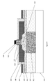
- such methods epitaxially grow raised base structures on the base region and the extrinsic base regions. More specifically, as shown in FIG. 7 , such methods epitaxially grow raised base structures 340 / 342 on the base region 310 and the extrinsic base regions 312 .
- such methods first grow a first layer 340 of the raised base structures 340 / 342 to have a first concentration of doping material on the base region 310 and the extrinsic base regions 312 .
- the methods grow the upper layer 342 of the raised base structures 340 / 342 to have a second concentration of the doping material on the first layer 340 of the raised base structures 340 / 342 .
- the second concentration of doping material is higher than the first concentration of the doping material.
- such methods simultaneously form raised base limiting structures 320 / 326 over portions of the extrinsic base regions 312 that are distal to the base region 310 .
- the raised base structures 340 / 342 extend on the extrinsic base regions 312 in a direction from the base region 310 only to where the raised base limiting structures 320 / 326 are positioned (on the distal portions of the extrinsic base regions 312 ).
- the “raised base limiting structures” 320 / 326 limit the size of the raised base structures 340 / 342 (limit how far from the base region 310 the raised base structures 340 / 342 extend from the center of the base region 310 ).
- the base region 310 has an upper surface connected to the sidewall spacers 326 by an oxide.
- the upper layer 342 of the raised base structures 340 / 342 is the surface opposite the location where the raised base structures 340 / 342 contact the base region 310 (the upper surface of the base region 310 ) and opposite the location where the raised base structures 340 / 342 contact the extrinsic base regions 312 .
- the sidewall spacers 326 extend a first distance from the upper surface of the base region 310 and the raised base structures 340 / 342 extend a second (lesser) distance from the upper surface of the base region 310 , such that the sidewall spacers 326 are taller than the raised base structures 340 / 342 (when measured from the upper surface of the base region 310 ).
- such methods then oxidized the upper layer of the raised base structures. More specifically, as shown in FIG. 8 , these methods oxidize the upper layer 342 of the raised base structures 340 / 342 .
- the oxidation process can be a high-pressure oxidization (HiPOX) process, or other similar process.
- HiPOX high-pressure oxidization
- the high-pressure oxidation process can be generally performed at lower temperatures than normal oxidation processes (because of the additional pressure utilized) and can use steam in the oxidation process.
- the higher doping in the upper layer 342 of the raised base structures helps increase oxidation during this oxidation processing.
- the oxidizing of the upper layer 342 of the raised base structures 340 / 342 forms an isolation layer 350 .
- the upper surface of the isolation layer 350 is flat (planar) and generally (within 5-20 degrees) parallel to the upper surface of the base region 310 .
- the epitaxial growth process of the raised base structures 340 / 342 naturally forms a planar surface without additional processing steps, and the subsequent oxidation process maintains this planar surface shape, thereby forming a planar isolation layer 350 that does not need to be polished or planarized. Therefore, these structures are sometimes referred to herein as “self-planarizing isolation raised base structures.”
- These self-planarizing isolation raised base structures 320 / 326 do not require any additional processing (such as chemical mechanical planarization (CMP)) to become planar; instead, the epitaxial process and the oxidation process themselves create a planar surface without any additional processing steps.
- CMP chemical mechanical planarization
- the methods then remove the sacrificial emitter and cap. More specifically, as shown in FIGS. 9 and 10 , such methods remove the cap and sacrificial emitter structure 322 (including the underlying oxide) to leave an open space between the sidewall spacers 326 and to expose the base region 310 through the open space between the sidewall spacers 326 .
- the material removal processes used in FIGS. 9-10 can be continuous or separate processes and are selective to the materials used for the cap 324 , sacrificial emitter 322 and oxide 320 ; however, such material removal processes are controlled so that they do not substantially affect the conformal layer 326 , the isolation layer 350 , or the material of the collector 302 .
- the methods form the final emitter structure. More specifically, as shown in FIG. 11 , these methods form an emitter 360 within the open space between the sidewall spacers 326 that directly contacts the upper surface of the base region 310 .
- This processing can deposit a pre-doped material (in-situ doped material) or a material that is first deposited or grown, and subsequently doped.
- the emitter will have the same doping polarity as the collector (but will be more heavily doped) and will have a polarity opposite that of the base.
- the various patterning processes discussed above are also used here to limit the shape and size of the emitter 360 . These processes form the emitter 360 , as shown in the drawings, such that the emitter 360 extends over the sidewall spacers 326 on to the raised base structures 340 / 342 . However, this does not affect the performance of the device because the isolation layer 350 electrically insulates the emitter 360 from the raised base structures 340 / 342 .
- the same pattern used to form the photoresist structures 330 can be used with an opposite type of photoresist to form photoresist 332 .
- selective material removal processing is again used to remove the raised base limiting structures 320 / 326 , as shown in FIG. 13 .
- the photoresist 332 is removed revealing the final structure, that is ready for overlying isolation layers and contact formation processing well-known to those ordinarily skilled in the art.
- Such methods produce various integrated circuit structures (such as PNP or NPN bipolar junction transistors).
- Such integrated circuit structures include a collector region 302 within a substrate 300 between insulator regions (shallow trench isolation (STI) regions).
- An epitaxial base material is positioned on the collector region 302 and the insulator regions.
- This epitaxial base material comprises a base region 310 on the collector region 302 and comprises extrinsic base regions 312 on the insulator regions.
- an emitter 360 is positioned on the base region 310 .
- the emitter 360 has sidewalls perpendicular to the bottom surface of the emitter 360 that contacts the base region 310 .
- the integrated circuit structure includes sidewall spacers 326 on the sidewalls of the emitter 360 .
- epitaxial raised base structures 340 / 342 are positioned on the base region 310 and the extrinsic base regions 312 .
- the raised base structures 340 / 342 comprise a lower first layer 340 on the base region 310 and the extrinsic base regions 312 , and an upper layer 342 on the first layer 340 of the raised base structures 340 / 342 .
- the upper layer 342 of the raised base structures 340 / 342 is opposite the location where the raised base structures 340 / 342 contact the base region 310 and the extrinsic base regions 312 .
- the lower first layer 340 of the raised base structures 340 / 342 has a first concentration of doping material
- the upper layer 342 of the raised base structures 340 / 342 has a second concentration of the doping material that is higher than the first concentration of the doping material
- the integrated circuit structure further includes raised base limiting structures 320 / 326 on distal portions of the extrinsic base regions 312 that are distal to the base region 310 .
- the raised base limiting structures 320 / 326 can be retained in the final structure.
- the raised base structures 340 / 342 extend on the extrinsic base regions 312 in a direction from the base region 310 only to where the raised base limiting structures 320 / 326 are positioned on the distal portions of the extrinsic base regions 312 . Therefore, the raised base limiting structures 320 / 326 are positioned on distal portions of the extrinsic base regions 312 to limit the size of the raised base structures 340 / 342 .
- the base region 310 has an upper surface connected to the sidewall spacers 326 by an oxide.
- the sidewall spacers 326 extend a first distance from the upper surface of the base region 310 .
- the upper layer 342 of the raised base structures 340 / 342 is parallel to the upper surface of the base region 310 .
- the upper layer 342 of the raised base structures 340 / 342 extends a second distance from the upper surface of the base region 310 that is less than the first distance, such that the sidewall spacers 326 are taller than the raised base structures 340 / 342 (when measured from the upper surface of the base region 310 ).
- the sidewall spacers 326 have distal ends extending a first distance from the upper surface of the base region 310 and the emitter 360 extends a second (greater) distance from the upper surface of the base region 310 .
- the emitter 360 extends over the sidewall spacers 326 on to the raised base structures 340 / 342 ; however, the isolation layer 350 electrically insulates the emitter 360 from the raised base structures 340 / 342 .
- the methods described above are used in the fabrication of integrated circuit chips.
- the resulting integrated circuit chips can be distributed by the fabricator in raw wafer form (that is, as a single wafer that has multiple unpackaged chips), as a bare die, or in a packaged form.
- the chip is mounted in a single chip package (such as a plastic carrier, with leads that are affixed to a motherboard or other higher level carrier) or in a multichip package (such as a ceramic carrier that has either or both surface interconnections or buried interconnections).
- the chip is then integrated with other chips, discrete circuit elements, and/or other signal processing devices as part of either (a) an intermediate product, such as a motherboard, or (b) an end product.
- the end product can be any product that includes integrated circuit chips, ranging from toys and other low-end applications to advanced computer products having a display, a keyboard or other input device, and a central processor.
Landscapes
- Bipolar Transistors (AREA)
Abstract
Description
Claims (17)
Priority Applications (2)
| Application Number | Priority Date | Filing Date | Title |
|---|---|---|---|
| US13/890,341 US9202869B2 (en) | 2013-05-09 | 2013-05-09 | Self-aligned bipolar junction transistor having self-planarizing isolation raised base structures |
| US14/922,457 US20160043202A1 (en) | 2013-05-09 | 2015-10-26 | Self-aligned bipolar junction transistor having self-planarizing isolation raised base structures |
Applications Claiming Priority (1)
| Application Number | Priority Date | Filing Date | Title |
|---|---|---|---|
| US13/890,341 US9202869B2 (en) | 2013-05-09 | 2013-05-09 | Self-aligned bipolar junction transistor having self-planarizing isolation raised base structures |
Related Child Applications (1)
| Application Number | Title | Priority Date | Filing Date |
|---|---|---|---|
| US14/922,457 Division US20160043202A1 (en) | 2013-05-09 | 2015-10-26 | Self-aligned bipolar junction transistor having self-planarizing isolation raised base structures |
Publications (2)
| Publication Number | Publication Date |
|---|---|
| US20140332927A1 US20140332927A1 (en) | 2014-11-13 |
| US9202869B2 true US9202869B2 (en) | 2015-12-01 |
Family
ID=51864215
Family Applications (2)
| Application Number | Title | Priority Date | Filing Date |
|---|---|---|---|
| US13/890,341 Expired - Fee Related US9202869B2 (en) | 2013-05-09 | 2013-05-09 | Self-aligned bipolar junction transistor having self-planarizing isolation raised base structures |
| US14/922,457 Abandoned US20160043202A1 (en) | 2013-05-09 | 2015-10-26 | Self-aligned bipolar junction transistor having self-planarizing isolation raised base structures |
Family Applications After (1)
| Application Number | Title | Priority Date | Filing Date |
|---|---|---|---|
| US14/922,457 Abandoned US20160043202A1 (en) | 2013-05-09 | 2015-10-26 | Self-aligned bipolar junction transistor having self-planarizing isolation raised base structures |
Country Status (1)
| Country | Link |
|---|---|
| US (2) | US9202869B2 (en) |
Families Citing this family (1)
| Publication number | Priority date | Publication date | Assignee | Title |
|---|---|---|---|---|
| DE102016207536B4 (en) * | 2016-05-02 | 2020-03-19 | Infineon Technologies Dresden Gmbh | Method of manufacturing a bipolar transistor |
Citations (12)
| Publication number | Priority date | Publication date | Assignee | Title |
|---|---|---|---|---|
| US6667521B2 (en) | 2001-06-22 | 2003-12-23 | International Business Machines Corporation | Bipolar transistor with raised extrinsic base fabricated in an integrated BiCMOS circuit |
| US6777302B1 (en) | 2003-06-04 | 2004-08-17 | International Business Machines Corporation | Nitride pedestal for raised extrinsic base HBT process |
| US7037798B2 (en) | 2004-01-09 | 2006-05-02 | International Business Machines Corporation | Bipolar transistor structure with self-aligned raised extrinsic base and methods |
| US7288827B2 (en) | 2003-01-15 | 2007-10-30 | International Business Machines Corporation | Self-aligned mask formed utilizing differential oxidation rates of materials |
| US20070298578A1 (en) * | 2006-06-21 | 2007-12-27 | International Business Machines Corporation | Bipolar transistor with dual shallow trench isolation and low base resistance |
| US20080203490A1 (en) * | 2007-02-28 | 2008-08-28 | Feilchenfeld Natalie B | Bipolar transistor with raised extrinsic self-aligned base using selective epitaxial growth for bicmos integration |
| US7642168B1 (en) * | 2007-05-18 | 2010-01-05 | National Semiconductor Corporation | System and method for providing a self aligned bipolar transistor using a sacrificial polysilicon external base |
| US7696034B2 (en) | 2004-03-13 | 2010-04-13 | International Business Machines Corporation | Methods of base formation in a BiCOMS process |
| US7719031B2 (en) | 2003-07-11 | 2010-05-18 | Panasonic Corporation | Heterojunction biploar transistor and method for manufacturing same |
| US7776704B2 (en) | 2004-09-21 | 2010-08-17 | International Business Machines Corporation | Method to build self-aligned NPN in advanced BiCMOS technology |
| US7935986B2 (en) | 2005-07-06 | 2011-05-03 | International Business Machines Corporation | Method for forming a bipolar transistor device with self-aligned raised extrinsic base |
| US20110312147A1 (en) * | 2010-06-17 | 2011-12-22 | International Business Machines Corporation | Transistor structure with a sidewall-defined intrinsic base to extrinsic base link-up region and method of forming the transistor |
Family Cites Families (2)
| Publication number | Priority date | Publication date | Assignee | Title |
|---|---|---|---|---|
| US6867440B1 (en) * | 2002-08-13 | 2005-03-15 | Newport Fab, Llc | Self-aligned bipolar transistor without spacers and method for fabricating same |
| US8299500B2 (en) * | 2005-08-23 | 2012-10-30 | International Business Machines Corporation | Silicon germanium heterojunction bipolar transistor having interstitial trapping layer in base region |
-
2013
- 2013-05-09 US US13/890,341 patent/US9202869B2/en not_active Expired - Fee Related
-
2015
- 2015-10-26 US US14/922,457 patent/US20160043202A1/en not_active Abandoned
Patent Citations (14)
| Publication number | Priority date | Publication date | Assignee | Title |
|---|---|---|---|---|
| US6667521B2 (en) | 2001-06-22 | 2003-12-23 | International Business Machines Corporation | Bipolar transistor with raised extrinsic base fabricated in an integrated BiCMOS circuit |
| US7288827B2 (en) | 2003-01-15 | 2007-10-30 | International Business Machines Corporation | Self-aligned mask formed utilizing differential oxidation rates of materials |
| US6777302B1 (en) | 2003-06-04 | 2004-08-17 | International Business Machines Corporation | Nitride pedestal for raised extrinsic base HBT process |
| US7719031B2 (en) | 2003-07-11 | 2010-05-18 | Panasonic Corporation | Heterojunction biploar transistor and method for manufacturing same |
| US7037798B2 (en) | 2004-01-09 | 2006-05-02 | International Business Machines Corporation | Bipolar transistor structure with self-aligned raised extrinsic base and methods |
| US7696034B2 (en) | 2004-03-13 | 2010-04-13 | International Business Machines Corporation | Methods of base formation in a BiCOMS process |
| US7776704B2 (en) | 2004-09-21 | 2010-08-17 | International Business Machines Corporation | Method to build self-aligned NPN in advanced BiCMOS technology |
| US7935986B2 (en) | 2005-07-06 | 2011-05-03 | International Business Machines Corporation | Method for forming a bipolar transistor device with self-aligned raised extrinsic base |
| US20070298578A1 (en) * | 2006-06-21 | 2007-12-27 | International Business Machines Corporation | Bipolar transistor with dual shallow trench isolation and low base resistance |
| US7888745B2 (en) | 2006-06-21 | 2011-02-15 | International Business Machines Corporation | Bipolar transistor with dual shallow trench isolation and low base resistance |
| US20080203490A1 (en) * | 2007-02-28 | 2008-08-28 | Feilchenfeld Natalie B | Bipolar transistor with raised extrinsic self-aligned base using selective epitaxial growth for bicmos integration |
| US8236662B2 (en) | 2007-02-28 | 2012-08-07 | International Business Machines Corporation | Bipolar transistor with raised extrinsic self-aligned base using selective epitaxial growth for BiCMOS integration |
| US7642168B1 (en) * | 2007-05-18 | 2010-01-05 | National Semiconductor Corporation | System and method for providing a self aligned bipolar transistor using a sacrificial polysilicon external base |
| US20110312147A1 (en) * | 2010-06-17 | 2011-12-22 | International Business Machines Corporation | Transistor structure with a sidewall-defined intrinsic base to extrinsic base link-up region and method of forming the transistor |
Non-Patent Citations (1)
| Title |
|---|
| Liu, et al., "A Self-Aligned Sacrificial Emitter Process for High Performance SiGe HBT in BiCMOS," 2012 The Electrochemical Society, 2012, 1 page. |
Also Published As
| Publication number | Publication date |
|---|---|
| US20140332927A1 (en) | 2014-11-13 |
| US20160043202A1 (en) | 2016-02-11 |
Similar Documents
| Publication | Publication Date | Title |
|---|---|---|
| US8441084B2 (en) | Horizontal polysilicon-germanium heterojunction bipolar transistor | |
| US9553145B2 (en) | Lateral bipolar junction transistors on a silicon-on-insulator substrate with a thin device layer thickness | |
| US11127816B2 (en) | Heterojunction bipolar transistors with one or more sealed airgap | |
| CN107316889B (en) | Compact device structure of bipolar junction transistor | |
| US9269787B2 (en) | Base profile of self-aligned bipolar transistors for power amplifier applications | |
| TWI752599B (en) | Structure and manufacture method of heterojunction bipolar transistor with marker layer | |
| US11145725B2 (en) | Heterojunction bipolar transistor | |
| US11177347B2 (en) | Heterojunction bipolar transistor | |
| US20250006824A1 (en) | Transistor with wrap-around extrinsic base | |
| US8173524B1 (en) | Process for epitaxially growing epitaxial material regions | |
| TW202541606A (en) | Electrostatic device | |
| US9202869B2 (en) | Self-aligned bipolar junction transistor having self-planarizing isolation raised base structures | |
| US11855195B2 (en) | Transistor with wrap-around extrinsic base | |
| EP4216280A1 (en) | Vertical bipolar transistors on soi substrates with the collectors in the buried oxide | |
| US11322414B2 (en) | Concurrent manufacture of field effect transistors and bipolar junction transistors with gain tuning | |
| US11637181B2 (en) | Lateral bipolar transistors with polysilicon terminals | |
| US11804542B2 (en) | Annular bipolar transistors | |
| US11916135B2 (en) | Bipolar transistor | |
| US11837460B2 (en) | Lateral bipolar transistor | |
| US10170601B2 (en) | Structure and formation method of semiconductor device with bipolar junction transistor | |
| CN119653791A (en) | Bipolar transistor | |
| CN121357924A (en) | Vertical heterojunction bipolar transistor |
Legal Events
| Date | Code | Title | Description |
|---|---|---|---|
| AS | Assignment |
Owner name: INTERNATIONAL BUSINESS MACHINES CORPORATION, NEW Y Free format text: ASSIGNMENT OF ASSIGNORS INTEREST;ASSIGNORS:FEILCHENFELD, NATALIE B.;LIU, QIZHI;REEL/FRAME:030381/0602 Effective date: 20130501 |
|
| FEPP | Fee payment procedure |
Free format text: PAYER NUMBER DE-ASSIGNED (ORIGINAL EVENT CODE: RMPN); ENTITY STATUS OF PATENT OWNER: LARGE ENTITY Free format text: PAYOR NUMBER ASSIGNED (ORIGINAL EVENT CODE: ASPN); ENTITY STATUS OF PATENT OWNER: LARGE ENTITY |
|
| AS | Assignment |
Owner name: GLOBALFOUNDRIES U.S. 2 LLC, NEW YORK Free format text: ASSIGNMENT OF ASSIGNORS INTEREST;ASSIGNOR:INTERNATIONAL BUSINESS MACHINES CORPORATION;REEL/FRAME:036550/0001 Effective date: 20150629 |
|
| AS | Assignment |
Owner name: GLOBALFOUNDRIES INC., CAYMAN ISLANDS Free format text: ASSIGNMENT OF ASSIGNORS INTEREST;ASSIGNORS:GLOBALFOUNDRIES U.S. 2 LLC;GLOBALFOUNDRIES U.S. INC.;REEL/FRAME:036779/0001 Effective date: 20150910 |
|
| STCF | Information on status: patent grant |
Free format text: PATENTED CASE |
|
| AS | Assignment |
Owner name: WILMINGTON TRUST, NATIONAL ASSOCIATION, DELAWARE Free format text: SECURITY AGREEMENT;ASSIGNOR:GLOBALFOUNDRIES INC.;REEL/FRAME:049490/0001 Effective date: 20181127 |
|
| FEPP | Fee payment procedure |
Free format text: MAINTENANCE FEE REMINDER MAILED (ORIGINAL EVENT CODE: REM.); ENTITY STATUS OF PATENT OWNER: LARGE ENTITY |
|
| LAPS | Lapse for failure to pay maintenance fees |
Free format text: PATENT EXPIRED FOR FAILURE TO PAY MAINTENANCE FEES (ORIGINAL EVENT CODE: EXP.); ENTITY STATUS OF PATENT OWNER: LARGE ENTITY |
|
| STCH | Information on status: patent discontinuation |
Free format text: PATENT EXPIRED DUE TO NONPAYMENT OF MAINTENANCE FEES UNDER 37 CFR 1.362 |
|
| FP | Lapsed due to failure to pay maintenance fee |
Effective date: 20191201 |
|
| AS | Assignment |
Owner name: GLOBALFOUNDRIES INC., CAYMAN ISLANDS Free format text: RELEASE BY SECURED PARTY;ASSIGNOR:WILMINGTON TRUST, NATIONAL ASSOCIATION;REEL/FRAME:054636/0001 Effective date: 20201117 |
|
| AS | Assignment |
Owner name: GLOBALFOUNDRIES U.S. INC., NEW YORK Free format text: RELEASE BY SECURED PARTY;ASSIGNOR:WILMINGTON TRUST, NATIONAL ASSOCIATION;REEL/FRAME:056987/0001 Effective date: 20201117 Owner name: GLOBALFOUNDRIES U.S. INC., NEW YORK Free format text: RELEASE OF SECURITY INTEREST;ASSIGNOR:WILMINGTON TRUST, NATIONAL ASSOCIATION;REEL/FRAME:056987/0001 Effective date: 20201117 |