US9172024B2 - Ultrasound probe and method of manufacturing ultrasound probe - Google Patents
Ultrasound probe and method of manufacturing ultrasound probe Download PDFInfo
- Publication number
- US9172024B2 US9172024B2 US13/795,103 US201313795103A US9172024B2 US 9172024 B2 US9172024 B2 US 9172024B2 US 201313795103 A US201313795103 A US 201313795103A US 9172024 B2 US9172024 B2 US 9172024B2
- Authority
- US
- United States
- Prior art keywords
- wiring pattern
- width
- back face
- backing material
- intermediate layer
- Prior art date
- Legal status (The legal status is an assumption and is not a legal conclusion. Google has not performed a legal analysis and makes no representation as to the accuracy of the status listed.)
- Active, expires
Links
- 238000002604 ultrasonography Methods 0.000 title claims description 160
- 239000000523 sample Substances 0.000 title claims description 74
- 238000004519 manufacturing process Methods 0.000 title claims description 11
- 239000000758 substrate Substances 0.000 claims abstract description 119
- 239000000463 material Substances 0.000 claims abstract description 97
- 230000005855 radiation Effects 0.000 claims abstract description 27
- 239000010410 layer Substances 0.000 claims description 157
- 239000000853 adhesive Substances 0.000 claims description 21
- 230000001070 adhesive effect Effects 0.000 claims description 21
- 238000000034 method Methods 0.000 claims description 12
- 239000012790 adhesive layer Substances 0.000 claims description 5
- 238000012285 ultrasound imaging Methods 0.000 description 13
- 239000011133 lead Substances 0.000 description 6
- 230000000694 effects Effects 0.000 description 4
- 239000000843 powder Substances 0.000 description 4
- OKTJSMMVPCPJKN-UHFFFAOYSA-N Carbon Chemical compound [C] OKTJSMMVPCPJKN-UHFFFAOYSA-N 0.000 description 3
- 230000002452 interceptive effect Effects 0.000 description 3
- 230000002829 reductive effect Effects 0.000 description 3
- 239000004593 Epoxy Substances 0.000 description 2
- 229910004243 O3-PbTiO3 Inorganic materials 0.000 description 2
- 229910004293 O3—PbTiO3 Inorganic materials 0.000 description 2
- 229910002113 barium titanate Inorganic materials 0.000 description 2
- 230000005540 biological transmission Effects 0.000 description 2
- 239000000919 ceramic Substances 0.000 description 2
- 239000013078 crystal Substances 0.000 description 2
- 239000003822 epoxy resin Substances 0.000 description 2
- 229910002804 graphite Inorganic materials 0.000 description 2
- 239000010439 graphite Substances 0.000 description 2
- 229910052451 lead zirconate titanate Inorganic materials 0.000 description 2
- 239000000203 mixture Substances 0.000 description 2
- 230000010355 oscillation Effects 0.000 description 2
- 229920000647 polyepoxide Polymers 0.000 description 2
- 229920001721 polyimide Polymers 0.000 description 2
- WFKWXMTUELFFGS-UHFFFAOYSA-N tungsten Chemical compound [W] WFKWXMTUELFFGS-UHFFFAOYSA-N 0.000 description 2
- 230000002411 adverse Effects 0.000 description 1
- 230000003321 amplification Effects 0.000 description 1
- 230000002238 attenuated effect Effects 0.000 description 1
- JRPBQTZRNDNNOP-UHFFFAOYSA-N barium titanate Chemical compound [Ba+2].[Ba+2].[O-][Ti]([O-])([O-])[O-] JRPBQTZRNDNNOP-UHFFFAOYSA-N 0.000 description 1
- 229910052799 carbon Inorganic materials 0.000 description 1
- 238000005520 cutting process Methods 0.000 description 1
- 230000003247 decreasing effect Effects 0.000 description 1
- 230000003111 delayed effect Effects 0.000 description 1
- 239000011521 glass Substances 0.000 description 1
- PCHJSUWPFVWCPO-UHFFFAOYSA-N gold Chemical compound [Au] PCHJSUWPFVWCPO-UHFFFAOYSA-N 0.000 description 1
- 239000010931 gold Substances 0.000 description 1
- 229910052737 gold Inorganic materials 0.000 description 1
- HFGPZNIAWCZYJU-UHFFFAOYSA-N lead zirconate titanate Chemical compound [O-2].[O-2].[O-2].[O-2].[O-2].[Ti+4].[Zr+4].[Pb+2] HFGPZNIAWCZYJU-UHFFFAOYSA-N 0.000 description 1
- QSHDDOUJBYECFT-UHFFFAOYSA-N mercury Chemical compound [Hg] QSHDDOUJBYECFT-UHFFFAOYSA-N 0.000 description 1
- 229910052753 mercury Inorganic materials 0.000 description 1
- 239000002184 metal Substances 0.000 description 1
- 229910052751 metal Inorganic materials 0.000 description 1
- 229910044991 metal oxide Inorganic materials 0.000 description 1
- 150000004706 metal oxides Chemical class 0.000 description 1
- 238000012986 modification Methods 0.000 description 1
- 230000004048 modification Effects 0.000 description 1
- 238000000465 moulding Methods 0.000 description 1
- 238000003199 nucleic acid amplification method Methods 0.000 description 1
- 230000000149 penetrating effect Effects 0.000 description 1
- 229920000334 poly[3-(3'-N,N,N-triethylamino-1-propyloxy)-4-methylthiophene-2,5-diyl hydrochloride] polymer Polymers 0.000 description 1
- 239000004800 polyvinyl chloride Substances 0.000 description 1
- 229920000915 polyvinyl chloride Polymers 0.000 description 1
- 229910052594 sapphire Inorganic materials 0.000 description 1
- 239000010980 sapphire Substances 0.000 description 1
- 239000002356 single layer Substances 0.000 description 1
- 238000003892 spreading Methods 0.000 description 1
- 238000006467 substitution reaction Methods 0.000 description 1
- 229910052721 tungsten Inorganic materials 0.000 description 1
- 239000010937 tungsten Substances 0.000 description 1
- 229910000859 α-Fe Inorganic materials 0.000 description 1
Images


Classifications
-
- H—ELECTRICITY
- H10—SEMICONDUCTOR DEVICES; ELECTRIC SOLID-STATE DEVICES NOT OTHERWISE PROVIDED FOR
- H10N—ELECTRIC SOLID-STATE DEVICES NOT OTHERWISE PROVIDED FOR
- H10N30/00—Piezoelectric or electrostrictive devices
- H10N30/1071—Piezoelectric or electrostrictive devices with electrical and mechanical input and output, e.g. having combined actuator and sensor parts
-
- H01L41/0825—
-
- B—PERFORMING OPERATIONS; TRANSPORTING
- B06—GENERATING OR TRANSMITTING MECHANICAL VIBRATIONS IN GENERAL
- B06B—METHODS OR APPARATUS FOR GENERATING OR TRANSMITTING MECHANICAL VIBRATIONS OF INFRASONIC, SONIC, OR ULTRASONIC FREQUENCY, e.g. FOR PERFORMING MECHANICAL WORK IN GENERAL
- B06B1/00—Methods or apparatus for generating mechanical vibrations of infrasonic, sonic, or ultrasonic frequency
- B06B1/02—Methods or apparatus for generating mechanical vibrations of infrasonic, sonic, or ultrasonic frequency making use of electrical energy
- B06B1/06—Methods or apparatus for generating mechanical vibrations of infrasonic, sonic, or ultrasonic frequency making use of electrical energy operating with piezoelectric effect or with electrostriction
- B06B1/0607—Methods or apparatus for generating mechanical vibrations of infrasonic, sonic, or ultrasonic frequency making use of electrical energy operating with piezoelectric effect or with electrostriction using multiple elements
- B06B1/0622—Methods or apparatus for generating mechanical vibrations of infrasonic, sonic, or ultrasonic frequency making use of electrical energy operating with piezoelectric effect or with electrostriction using multiple elements on one surface
-
- H01L41/25—
-
- H—ELECTRICITY
- H10—SEMICONDUCTOR DEVICES; ELECTRIC SOLID-STATE DEVICES NOT OTHERWISE PROVIDED FOR
- H10N—ELECTRIC SOLID-STATE DEVICES NOT OTHERWISE PROVIDED FOR
- H10N30/00—Piezoelectric or electrostrictive devices
- H10N30/01—Manufacture or treatment
- H10N30/03—Assembling devices that include piezoelectric or electrostrictive parts
-
- Y—GENERAL TAGGING OF NEW TECHNOLOGICAL DEVELOPMENTS; GENERAL TAGGING OF CROSS-SECTIONAL TECHNOLOGIES SPANNING OVER SEVERAL SECTIONS OF THE IPC; TECHNICAL SUBJECTS COVERED BY FORMER USPC CROSS-REFERENCE ART COLLECTIONS [XRACs] AND DIGESTS
- Y10—TECHNICAL SUBJECTS COVERED BY FORMER USPC
- Y10T—TECHNICAL SUBJECTS COVERED BY FORMER US CLASSIFICATION
- Y10T29/00—Metal working
- Y10T29/42—Piezoelectric device making
Definitions
- the embodiments of the present invention relates to an ultrasound probe and a method of manufacturing an ultrasound probe.
- An ultrasound imaging apparatus obtains biological information by scanning a subject through an ultrasound probe. Moreover, the ultrasound imaging apparatus images the state within the subject based on the obtained biological information. That is, the ultrasound imaging apparatus sends a control signal regarding the scanning of the ultrasound waves to the ultrasound probe. Based on the control signal, ultrasound waves are sent to the subject through the ultrasound probe. In addition, the ultrasound probe receives reflected waves from the subject. Based on these reflected waves, the ultrasound imaging apparatus acquires biological information based on the state within the subject. Moreover, the ultrasound imaging apparatus creates an ultrasound image based on this biological information.
- An ultrasound probe has, for example, the following configuration.
- the ultrasound probe comprises a piezoelectric transducer group with a 1-dimensional array or 2-dimensional array.
- On the side facing the radiation direction (acoustic radiation direction) of the ultrasound waves in said piezoelectric transducer group (hereinafter referred to as the “front face side”), an acoustic matching layer is placed with an electrode in between.
- the acoustic matching layer is placed for the purpose of matching the acoustic impedance of the piezoelectric transducer and the acoustic impedance of a biological object.
- a backing material On the side facing the direction opposite the radiation direction of the ultrasound waves in the piezoelectric transducer (hereinafter referred to as the “back face side”), a backing material is placed with an electrode and FPC (Flexible Printed Circuit) in between. Moreover, an intermediate layer with electric conductivity may be placed between the piezoelectric transducer and the backing material.
- FPC Flexible Printed Circuit
- the ultrasound waves irradiated to the back face side of the piezoelectric transducer are attenuated and absorbed by the backing material.
- the structure of, for example, the piezoelectric transducer is supported by the backing material.
- the intermediate layer has higher acoustic impedance than the piezoelectric transducer, and is provided to enhance the radiation efficiency of the ultrasound waves. Due to the gap between the acoustic impedance of the intermediate layer and the acoustic impedance of the piezoelectric transducer, the ultrasound waves irradiated to the back face side of the piezoelectric transducer are reflected by these interfaces.
- the ultrasound waves are sent out to the ultrasound wave radiation plane side that is the front face of the piezoelectric transducer.
- a wiring pattern (electrode lead) is provided on the piezoelectric transducer side of the FPC. Through the wiring pattern of the FPC, an electric signal is sent from the subsequent circuit to the piezoelectric transducer. Moreover, through the wiring pattern of the FPC, an electric signal is drawn from the piezoelectric transducer to the subsequent circuit.
- the FPC is placed on the front face side in the backing material.
- This FPC is, for example, placed substantially parallel to the backing material so as to cover the front face side of the backing material.
- the FPC is folded toward the subsequent circuit side (the side opposite the piezoelectric transducer) at the end of the front face of the backing material, and extended toward the subsequent circuit side. If the FPC is not folded toward the subsequent circuit side at the end of the front face of the backing material, the FPC spreads in the array direction or lens direction in the ultrasound transducer. By preventing the FPC from spreading, the ultrasound probe is prevented from becoming larger.
- folding the FPC at the end of the front face of the backing material is also for the purpose of improving the impact resistance.
- the FPC and the construct are adhered to each other using an adhesive in order to improve the reliability of the connection.
- This construct may hereinafter be referred to as the “intermediate layer, etc.”
- the side (the surface substantially parallel to the radiation direction of the ultrasound waves) of each intermediate layer, etc., in a 1D alignment or 2D alignment and the front face of the FPC are adhered (see, for example, Patent Document 1/FIG. 2, reference 140). That is, there is no adhesive layer on the plane in which each intermediate layer, etc., is facing the FPC.
- the adhesive layer is provided in the position at which the intermediate layer, etc., on further end of the element alignment is adjacent to the front face of the FPC. That is, one interface to be bonded with the adhesive is the end of the side of the intermediate layer, etc., while the other interface is the face of the FPC facing the radiation direction of the ultrasound waves.
- the above-mentioned FPC has a risk of breakage due to being folded. Consequently, there is a risk of breakage (such as disconnection) of the wiring pattern in the FPC.
- a risk of breakage such as disconnection
- the wiring pattern is folded in the state bonded to the adhesive that has been set. Consequently, a force may be applied to the wiring pattern in the direction of resistance to the bonded state by the adhesive to cause a breakage.
- a coverlay (film, covering material) using, for example, a polyimide film may be provided on said folded section. This coverlay protects the wiring pattern.
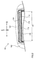
- FIG. 1 is a schematic perspective view illustrating an ultrasound probe according to the embodiment.
- FIG. 2 is a schematic view of the ultrasound probe in the cross-section shown in FIG. 1 .
- FIG. 3 is a schematic perspective view illustrating the ultrasound transducer of the ultrasound probe according to the first embodiment.
- FIG. 4 is a schematic view illustrating the ultrasound transducer along A-A′ in FIG. 3 .
- FIG. 5 is a schematic view illustrating the manufacturing process of the ultrasound transducer.
- FIG. 6 is a schematic view illustrating the ultrasound transducer according to the first variation.
- FIG. 7 is a schematic perspective view illustrating the ultrasound transducer of the ultrasound probe according to the second embodiment.
- FIG. 8 is a schematic view illustrating the ultrasound transducer along B-B′ of FIG. 7 .
- the ultrasound probe comprises a piezoelectric transducer, a backing material, and a flexible substrate.
- the piezoelectric transducer has electrodes on each of a front face facing the radiation direction of ultrasound waves and a back face facing the opposite direction.
- the backing material is provided on the back face side of the piezoelectric transducer, and has a first width substantially equal to the width of the piezoelectric transducer widthwise and perpendicular to the radiation direction of the ultrasound waves.
- the flexible substrate is located between the backing material and the piezoelectric transducer, with a wiring pattern provided on the face on the piezoelectric transducer side. In addition, the flexible substrate is folded in a direction substantially opposite the radiation direction around an end of the backing material widthwise.
- the wiring pattern of the flexible substrate is covered by a covering member.
- the front face of the layer located on the front face side with regard to the wiring pattern has a width substantially equal to said first width and the back face of this layer is formed to have a second width shorter than said first width.
- a space is provided between this layer and the backing material due to the difference between the first width and the second width of this layer.
- the covering member covers the wiring pattern extending at least from the folded section of the flexible substrate into the space.
- the ultrasound transducer, its manufacturing method and the ultrasound probe according to the embodiment will hereinafter be described with reference to FIG. 1-FIG . 8 .
- FIG. 1 is a schematic perspective view illustrating the ultrasound probe 10 according to the embodiment.
- FIG. 2 is a schematic view of the ultrasound probe 10 in the cross-section shown in FIG. 1 .
- FIG. 3 is a schematic perspective view schematically illustrating the ultrasound transducer 100 according to the first embodiment.
- the ultrasound probe 10 shown in FIG. 1 is one example, but may be an ultrasound probe of another type.
- FIG. 2 a drawing of the detailed configuration of the ultrasound transducer 100 is omitted.
- the shape of the overall element alignment of the ultrasound transducer 100 and the number of alignments of piezoelectric bodies 114 shown in FIG. 3 are also exemplary only. That is, a configuration other than the example shown in FIG. 3 may be applied.
- drawings of the space between an intermediate layer 116 and a back face substrate 120 , a wiring pattern 121 , and an adhesive 128 used for adhesion of the intermediate layer 116 and the back face substrate 120 are omitted.
- the direction from a backing material 118 to a first acoustic matching layer 110 is referred to as the “forward” direction.
- the direction opposite the forward direction is referred to as the “backward” direction.
- the face facing the forward direction of each component in the ultrasound transducer 100 is referred to as the “front face.”
- the face facing the backward direction is referred to as the “back face.”
- the ultrasound probe 10 is configured to include a probe case 103 supporting an acoustic lens 102 that is a subject contact surface.
- the ultrasound probe 10 is configured to include a cable 104 connected to the opposite side of the acoustic lens 102 in the probe case 103 .
- the ultrasound transducer 100 is provided having, for example, the piezoelectric transducer 114 .
- the ultrasound transducer 100 of this embodiment exemplified in FIG. 3 is configured to include the first acoustic matching layer 110 , a second acoustic matching layer 111 , the piezoelectric transducer 114 , the intermediate layer 116 , the backing material 118 , the back face substrate 120 , a front face substrate 124 , etc. Additionally, in the example of FIG. 3 , the piezoelectric transducer 114 is aligned in one dimension. Moreover, the second acoustic matching layer 111 is provided on the front face side of each piezoelectric transducer 114 . Furthermore, the first acoustic matching layer 110 is provided on the front face side of the second acoustic matching layer 111 .
- the intermediate layer 116 and the backing material 118 are provided in this order.
- the back face substrate 120 is provided between the backing material 118 and the intermediate layer 116 of the piezoelectric transducer 114 .
- the back face substrate 120 is at least drawn to the subsequent circuit such as a transmitting/receiving circuit.
- a drawing of the back face substrate 120 is partially omitted.
- the front face substrate 124 is provided on the front face side of the first acoustic matching layer 110 . Further, the acoustic lens 102 is provided on the front face side of the front face substrate 124 . As with the back face substrate 120 , the front face substrate 124 in FIG. 2 is omitted in the portion extending to the subsequent circuit. Moreover, a front face electrode is provided on the front face of the piezoelectric transducer 114 , where the front face electrode is adjacent to the back face of the second acoustic matching layer 111 . Furthermore, a back face electrode is provided on the back face of the piezoelectric transducer 114 . The back face electrode is adjacent to the front face of the intermediate layer 116 .
- each of the components comprising the ultrasound transducer 100 will be respectively described.
- the piezoelectric transducer 114 converts the voltage applied to the back face electrode and the front face electrode into ultrasound pulses. These ultrasound pulses are transferred to the subject. In addition, the piezoelectric transducer 114 receives the reflected waves from the subject and converts them into a voltage.
- the piezoelectric transducer 114 in general, PZT (lead zirconate titanate/Pb (Zr,Ti) O3), barium titanate (BaTiO3), PZNT (Pb (Zn1 ⁇ 3Nb2 ⁇ 3) O3-PbTiO3) single crystal, or PMNT (Pb (Mg1 ⁇ 3Nb2 ⁇ 3) O3-PbTiO3) single crystal, etc., can be used.
- the acoustic impedance of the piezoelectric transducer 114 may be made to, for example, about 30 Mrayl.
- the thickness of the piezoelectric transducer 114 into the thickness of ⁇ /4 of a wavelength of the ultrasound waves, it is possible to be less susceptible to the influence on the back face side. While the piezoelectric transducer 114 shown in FIGS. 2-4 is configured as a single layer, this is one example and a piezoelectric transducer 114 with multiple layers can also be configured.
- the first acoustic matching layer 110 and the second acoustic matching layer 111 are for matching the acoustic impedance between the piezoelectric transducer 114 and the subject. To this end, the first acoustic matching layer 110 and the second acoustic matching layer 111 are placed between the piezoelectric transducer 114 and the front face substrate 124 (see FIG. 3 ). For the first acoustic matching layer 110 and the second acoustic matching layer 111 , materials of different acoustic impedance are used. For example, the impedance of the first acoustic matching layer 110 is about 4-7 Mrayl.
- the impedance of the second acoustic matching layer 111 is, for example, about 9-15 Mrayl. Such a configuration allows the acoustic impedance to be changed stepwise between the piezoelectric transducer 114 and the acoustic lens 102 , and allows acoustic matching with the subject to be achieved.
- the first acoustic matching layer 110 and the second acoustic matching layer 111 are made of a material with electric conductivity in order to provide a conductive connection between the front face electrode of the piezoelectric transducer 114 and the front face substrate 124 .
- a conduction path is formed between at least either of the first acoustic matching layers 110 and the second acoustic matching layer 111 .
- the material for the first acoustic matching layer 110 having such a condition for example, carbon (isotropic graphite or graphite) can be used.
- carbon isotropic graphite or graphite
- the second acoustic matching layer 111 machinable glass, machinable ceramics, a mixture of epoxy and metal oxide powder, a mixture of epoxy and metal powder, etc. can be used.
- the thickness of the second acoustic matching layer 111 (the length in the forward-backward direction) is, for example, 150 ⁇ m-200 ⁇ m.
- the front face substrate 124 is, for example, an FPC (Flexible Printed Circuits) or an electric-conductive sheet, and each has a length extending to the subsequent circuit such as a transmitting/receiving circuit.
- a wiring pattern (connection lead/not shown) to be connected to, for example, the subsequent circuit is provided at least on the back face side of the front face substrate 124 .
- the front face substrate 124 is placed between the first acoustic matching layer 110 and the acoustic lens 102 .
- the wiring pattern on the front face substrate 124 is conductively connected to the front face of the piezoelectric transducer 114 through the first acoustic matching layer 110 and the second acoustic matching layer 111 .
- the conduction path provided to the first acoustic matching layer 110 or the second acoustic matching layer 111 is electrically connected to the front face electrode through the first acoustic matching layer 110 or the second acoustic matching layer 111 itself having electric conductivity.
- the backing material 118 absorbs the ultrasound pulses reflected in the direction (backward) opposite the radiation direction of the ultrasound waves and suppresses excess oscillation of each piezoelectric transducer 114 .
- the reflection from the back face of each piezoelectric transducer 114 during oscillation is suppressed by the backing material 118 . Consequently, it is possible to prevent the transmission/reception of the ultrasound pulses from being adversely affected.
- the backing material 118 any material may be used in terms of the acoustic attenuation, acoustic impedance, etc.
- epoxy resin or polyvinyl chloride including PUT powder or tungsten powder, rubber filled with ferrite powder, or porous ceramics immersed with epoxy resin or the like may be used.
- the acoustic impedance of the backing material 118 may be made to, for example, approximately 2 Mrayl-7 Mrayl.
- the width W 1 in the lens direction herein refers to the length of the backing material 118 perpendicular to the radiation direction of the ultrasound waves (see the direction E in FIGS. 1-4 ) and the alignment direction of the piezoelectric transducer 114 (see array direction; the direction A in FIGS. 1-4 ).
- this length may hereinafter be described as simply the “width in the lens direction” or “width.”
- the width W 1 of the backing material 118 in the lens direction is determined corresponding to the width of the piezoelectric transducer 114 and the intermediate layer 116 and the like in the same direction.
- the width W 1 of the backing material 118 in the lens direction is approximately equal to the width of the piezoelectric transducer 114 , etc., in the same direction.
- the width W 1 is substantially equal to the width of the piezoelectric transducer 114 in the lens direction means that, for the case in which the subject contact portion of the ultrasound probe 10 is affected by the width W 1 , the subject contact portion substantially does not become larger due to the width W 1 of the backing material 118 .
- the width W 1 may be slightly narrower or broader than the width of the piezoelectric transducer 114 .
- the length of the subject contact portion (subject contact surface) of the ultrasound probe 10 may be affected by the structure of the ultrasound transducer 100 within the portion.
- the back face substrate 120 is folded back towards the subsequent circuit at the end of the backing material 118 widthwise. Accordingly, the space for placing the back face substrate 120 thus folded back at the end affects the width in the lens direction.
- the space for placing the front face substrate 124 also affects the width in the lens direction.
- the side of the acoustic lens 102 is placed within the probe case 103 on the forward side of the ultrasound probe 10 , and furthermore, the face substrate 120 and the front face substrate 124 folded back as described above are placed within the lens. Therefore, the width of the ultrasound probe 10 in the lens direction (slice direction) is increased or decreased in proportion to each of the width of the backing material 118 (or the first acoustic matching layer 110 ), the width of the space for placing each folded substrate ( 120 , 124 ), the width of the side of the acoustic lens 102 , and the width of the probe case 103 .
- the width W 1 of the backing material 118 of the present embodiment in the lens direction is determined corresponding to the width of the piezoelectric transducer 114 , etc. Consequently, it is possible to prevent the subject contact portion of the ultrasound probe 10 from becoming larger.
- a step is provided on the back face of the intermediate layer 116 . That is, a step is provided for housing a coverlay 122 between the back face of the intermediate layer 116 and the back face substrate 120 . Its configuration will be described below.
- FIG. 4 is a schematic view along A-A′ in FIG. 3 .
- FIG. 5 is a schematic view illustrating the manufacturing process of the ultrasound transducer 100 . Note that the forward structure (piezoelectric transducer 114 , etc.) relative to the intermediate layer 116 is omitted in FIG. 5 .
- said space portion in order to explain the space portion, said space portion is emphasized and the ratio of the thickness relative to the overall thickness is shown as having increased.
- the height of the space and the thickness of the adhesive 128 are formed to be less than or equal to the thickness of the back face substrate 120 and the wiring pattern 121 .
- the intermediate layer 116 is provided adjacent to the back face of the piezoelectric transducer 114 and in contact with a back face electrode of the piezoelectric transducer 114 . Additionally, the intermediate layer 116 is configured to have higher acoustic impedance than that of the piezoelectric transducer 114 and the backing material 118 . Furthermore, its thickness (i.e., its length in the radiation direction E of the ultrasound waves) may be substantially 1 ⁇ 4 the wavelength of the ultrasound waves irradiated from the ultrasound transducer 100 . Moreover, as a material for the intermediate layer 116 , gold, lead, tungsten, mercury, sapphire, etc. may be used.
- the front face substrate 120 is, for example, the FPC and each has a length extending to a subsequent circuit such as a transmitting/receiving circuit.
- a wiring pattern 121 is provided on at least the front face side of the back face substrate 120 .
- the wiring pattern 121 on the back face substrate 120 is conductively connected to a back face electrode of the piezoelectric transducer 114 via the intermediate layer 116 .
- the wiring pattern 121 and the back face electrode are electrically connected through a conduction path provided penetrating the surface or the inside of the intermediate layer 116 .
- the wiring pattern 121 and the back face electrode may be electrically connected through the intermediate layer 116 itself.
- the wiring pattern 121 on the back face substrate 120 is connected to a subsequent circuit such as a transmitting/receiving circuit.
- the thickness of the substrate (base) portion is, for example, 20-50 ⁇ m
- the thickness of the electrode and the wiring pattern 121 can be 10-20 ⁇ m.
- the thickness of the coverlay 122 may be 20-50 ⁇ m.
- the center of the back face of the intermediate layer 116 is formed in a convex shape protruding backward. That is, a cutout is provided with the intermediate layer 116 on the back face side (the surface adjacent to the back face substrate 120 ) from both sides of the intermediate layer 116 towards the centerline of the intermediate layer 116 along the forward-backward direction of the ultrasound transducer 100 .
- the intermediate layer 116 is formed to have a first width X 1 (see FIG.
- a step is formed on the back face of the intermediate layer 116 due to the difference between the first width X 1 on the forward side and the second width X 2 on the back side.
- This step has an end surface protruding backwards on the center side of the back face or the intermediate layer 116 , and is also located on the forward side from this end surface.
- the step also has an opposing surface facing the back face substrate 120 at a predetermined interval.
- the wiring pattern 121 on the front face of the back face substrate 120 is covered with the coverlay (film, covering material) 122 made of, for example, a polyimide film.
- the coverlay 122 made of, for example, a polyimide film.
- the intermediate layer 116 and the back face substrate 120 may be adhered (see the right side of FIG. 5 ) before folding the back face substrate 120 (see the left side of FIG. 5 ).
- coverlay 122 is protecting the wiring pattern 121 , it is possible to avoid the situation in which a breakage occurs in the wiring pattern 121 by such a process.
- coverlay 122 corresponds to an example of the “covering member.”
- the coverlay 122 covers the folded section for protecting the wiring pattern 121 . Moreover, the coverlay 122 covers the portion between a pair of folded sections of the back face substrate 120 , i.e., the portion parallel to the front face of the backing material 118 . This is for the purpose of ensuring the protection of the folded section corresponding to the end or the backing material 118 widthwise by using the coverlay.
- the coverlay 122 is not provided in the area at which the wiring pattern 121 is in direct contact with the intermediate layer 116 . That is, the coverlay 122 is provided so as to sandwich the surface where the wiring pattern 121 is in direct contact with the intermediate layer 116 ( FIG.
- the coverlay 122 covers the area from the covering point on the folded section of the wiring pattern 121 to the point before reaching the end surface of the intermediate layer 116 on the back side.
- the height of the step Z 1 on the back face of the intermediate layer 116 is formed so as to be able to accommodate the thickness Z 2 of the coverlay 122 (Z 1 >Z 2 ).
- the height of the step refers to the length from the abovementioned end surface of the back face of the intermediate layer 116 to the opposing surface. Consequently, there is a predetermined interval Z 1 between the abovementioned opposing surface of the back face of the intermediate layer 116 and the front face of the back face substrate 120 .
- a portion of the coverlay 122 covering the wiring pattern 121 is housed in this space created between the step (opposing surface) of the intermediate layer 116 and the back face substrate 120 .
- Such an interval Z 1 may be, for example, approximately 25-55 ⁇ m when the thickness Z 2 of the coverlay 122 is 20-50 ⁇ m.
- the above-mentioned interval Z 1 that is the height of the space is determined so as not to interfere with the process of adhering the intermediate layer 116 , the back face substrate 120 and the backing material 118 . That is, the height of the step on the intermediate layer 116 (interval Z 1 ) is substantially slightly higher than the thickness of the coverlay 122 . This makes it possible to avoid the risk of interfering with the process of pressurized adhesion of the intermediate layer 116 , the back face substrate 120 and the backing material 118 .
- the coverlay 122 covers not only the folded section of the wiring pattern 121 but also the portion of the area in the wiring pattern 121 parallel to the front face of the backing material 118 from one folded section to the other folded section.
- the coverlay 122 does not interfere with the side of the intermediate layer 116 and is housed within the space. That is, the coverlay 122 extends by a predetermined length from one end of the backing material 118 widthwise to the other end on the opposite side, and the above-mentioned space is longer than at least the extended length in the extending direction.
- a step is provided to the intermediate layer 116 to create a space for housing the coverlay 122 extending from one end to the other of the backing material 118 between the front face of the back face substrate 120 .
- a space for placing the coverlay 122 on the front face of the backing material 118 can be ensured without making the width of the backing material 118 larger than the width of the piezoelectric transducer 114 or the intermediate layer 116 . Consequently, the width of the backing material 118 makes it possible to avoid the situation in which the subject contact portion of the ultrasound probe 10 is made larger.
- the intermediate layer 116 is bonded to the back face substrate 120 using an adhesive 128 .
- This adhesive 128 is in contact with the step consisting of the above-mentioned end surface and the opposing surface of the intermediate layer 116 .
- the adhesive 128 is in contact with the space for housing the coverlay 122 .
- the adhesive 128 is provided on the folded section of the back face substrate 120 . Therefore, the adhesive 128 provided, as shown in FIG. 5 , so as to be in contact with the opposing surface of the intermediate layer 116 , the side of the projecting portion, the wiring pattern 121 on the front face of the back face substrate 120 , and the coverlay 122 . In this way, the intermediate layer 116 is bonded to the back face substrate 120 .
- the present embodiment is not limited to such a configuration.
- the end surface may be connected to the wiring pattern 121 via an adhesive layer with electric conductivity.
- the acoustic characteristics and connection reliability between the intermediate layer 116 and the front face electrode may be improved.
- the intermediate layer 116 of the ultrasound transducer 100 is formed such that the back face side is in a convex shape as described above.
- the step on the intermediate layer 116 is formed by any method such as cutting, molding, etc.
- the wiring pattern 121 provided on the back face substrate 120 is covered by the coverlay 122 .
- This coverlay 122 covers the folded section of the wiring pattern 121 .
- the coverlay 122 covers a portion of the wiring pattern 121 provided from this folded section towards the other folded section.
- the coverlay 122 is not provided in the area at which the wiring pattern 121 is in contact with the end surface of the intermediate layer 116 . That is, as shown in FIG. 5 , in the area where the wiring pattern 121 is placed parallel to the backing material 118 , the area excluding the area in contact with the end surface of the intermediate layer 116 and its surrounding area (see area X 3 in FIG. 5 ) is covered by the coverlay 122 .
- the back face substrate 120 provided on the front face of the backing material 118 and the intermediate layer 116 formed in a convex shape are connected as follows. First, the back face substrate 120 and the intermediate layer 116 are made to face each other at a predetermined interval. Moreover, the adhesive 128 is provided in the space between the back face substrate 120 and the intermediate layer 116 , i.e., on both ends in the lens direction. After the adhesive 128 is provided to both ends, for example, pressurized adhesion is carried out. Consequently, the adhesive 128 enters the space between the back face substrate 120 and the intermediate layer 116 . The intermediate layer 116 is adhered to the back face substrate 120 with this adhesive 128 . At this point, as shown on the right side of FIG. 5 , the back face substrate 120 is in a state of not being folded.
- the adhesive 128 is provided on both of the abovementioned ends (space) and the adhesion process is carried out.
- the back face substrate 120 is folded at both ends of the backing material 118 .
- the coverlay 122 As the folded section of the wiring pattern 121 is covered by the coverlay 122 , the risk of breakage during the folding process is reduced.
- the ultrasound transducer 100 is provided within the ultrasound probe.
- the ultrasound probe has an interface (such as a cable) for electrically connecting the main body of the ultrasound imaging apparatus and the ultrasound probe.
- the ultrasound transducer 100 is also electrically connected to the main body of the ultrasound imaging apparatus through the wiring pattern on the front face substrate 124 and the wiring pattern on the back face substrate 120 as well as the interface on the ultrasound probe. That is, the main body and the ultrasound probe communicate a signal regarding the transmission/reception of the ultrasound waves between each other.
- a circuit substrate on which an electrical circuit such as a transmitting/receiving circuit is provided or a connection substrate for connecting the interface to the electronic circuit may be provided.
- signals are transmitted or received between the front face electrode or the back face electrode and the main body of the ultrasound imaging apparatus via the interface connecting the ultrasound probe to the main body, the wiring pattern of the connection substrate, the electronic circuit, or the wiring pattern on the front face substrate 124 or the back face substrate 120 .
- the main body of the ultrasound imaging apparatus sends an electric signal regarding the operational control of the ultrasound transducer 100 from its control unit to the ultrasound probe via the interface.
- This electric signal is sent to the electronic circuit in the circuit substrate via the connection substrate.
- the electronic circuit applies, based on the signal from the control unit in the main body of the ultrasound imaging apparatus, a voltage on the piezoelectric transducer 114 through the front face substrate 124 or the back face substrate 120 . In this way, the ultrasound pulses are sent to the subject.
- the ultrasound transducer 100 upon receiving the reflected waves from the subject, sends an electric signal, which has been converted by the piezoelectric transducer 114 , to the electronic circuit via, for example, the back face substrate 120 .
- the electronic circuit carries out a predetermined processing (delayed summation, amplification, etc.) on this electric signal and also sends the electric signal to the control unit in the main body of the ultrasound imaging apparatus via the connection circuit or the interface.
- the ultrasound imaging apparatus creates an ultrasound image. Note that the configuration may be such that the ultrasound probe is not provided with the electronic circuit.
- a step is provided to the intermediate layer 116 .
- the coverlay 122 covering the wiring pattern 121 is housed in this space. Therefore, it is possible to ensure a space for placing the coverlay 122 without expanding the width of the backing material 118 in the lens direction.
- the intermediate layer 116 is placed between the backing material 118 and the piezoelectric transducer 114 .
- the shape of the back face of the piezoelectric transducer 114 may be configured like the step of the above-mentioned intermediate layer 116 .
- the back face electrode is provided on the end surface of the projection at the step of the piezoelectric transducer 114 .
- the back face electrode may be provided on not only the end surface of the piezoelectric transducer 114 but also the opposing surface facing the back face substrate 120 .
- a material with electric conductivity may be used for the adhesive 128 .
- the configuration in which the intermediate layer 116 is provided as described above and a step is provided on the intermediate layer 116 may be more suitable.
- FIG. 6 is a schematic view illustrating the ultrasound transducer 100 according to the first variation.
- a space is provided on both ends in the lens direction of the back face of the intermediate layer 116 in the abovementioned embodiment.
- the back face substrate 120 is also folded at only one corresponding end as shown in FIG. 6 .
- FIG. 7 is a schematic perspective view illustrating the ultrasound transducer 100 of the ultrasound probe according to the second embodiment.
- the areas different from the first embodiment are mainly described and thus a description of the other overlapped areas is omitted.
- the number of elements of the ultrasound transducer 100 illustrated in FIG. 7 is not shown. The number of rows and the number of columns are also exemplary only, and another configuration may be applied.
- the ultrasound transducer 100 of this embodiment exemplified in FIG. 7 is, as in the first embodiment, configured to include a first acoustic matching layer 110 , a second acoustic matching layer 111 , a piezoelectric transducer 114 , an intermediate layer 116 , a backing material 118 , a back face substrate 120 , a front face substrate 124 , etc. Additionally, in one example of the second embodiment shown in FIG. 7 , the piezoelectric transducer 114 is aligned in one dimension.
- the back face substrate 120 is at least drawn to the subsequent circuit such as a transmitting/receiving circuit.
- a drawing of the back face substrate 120 is partially omitted.
- a drawing of the adhesive 128 is omitted.
- the back face substrate 120 is placed between the intermediate layer 116 and the backing material 118 .
- the back face substrate 120 in the second embodiment is folded towards the subsequent circuit side at both ends of the piezoelectric transducer 114 in the alignment direction (see the direction A in FIG. 7 ) rather than both ends of the backing material 118 in the lens direction.
- the alignment direction of the piezoelectric transducer 114 may hereinafter be referred to simply as the “array direction.”
- FIG. 8 is a schematic view illustrating the ultrasound transducer 100 along B-B′ of FIG. 7 .
- the elements shown on the left side are elements on one end of the element alignment.
- the elements shown on the right side in this figure are elements provided on the other end of the element alignment.
- the back face substrate 120 in the second embodiment is folded at both ends of the backing material 118 in the array direction. Therefore, the area of the wiring pattern 121 to be covered and protected by the coverlay 122 is the area corresponding to both of the above-mentioned ends.
- a step is provided on only the element on both ends of the alignment (intermediate layer 116 ).
- the step is provided only on one side corresponding to the folded section of the wiring pattern 121 , rather than on both sides.
- a step is provided to the intermediate layer 116 on both ends of the element alignment.
- this step is provided only on the portion of the back face of the intermediate layer 116 in proximity to the folded section of the wiring pattern 121 .
- a space is provided between the front face of the back face substrate 120 and the back face of the intermediate layer 116 .
- the coverlay 122 covering the wiring pattern 121 is housed in this space. Therefore, it is possible to ensure a space for placing the coverlay 122 without expanding the width of the backing material 118 in the array direction.
- the ultrasound probe 10 having the ultrasound transducer in a 1D array is described for both the first embodiment and the second embodiment. However, those embodiments can be applied to the ultrasound transducer in a 2D array.
- the folded section of the back face substrate 120 and the folded section of the front face substrate 124 are both consistent in the array direction or in the lens direction.
- the configuration in which a space is provided between the back face substrate 120 by a step can also be applied to the configuration in which the substrate is folded at one end in the lens direction as well as folded at the other end in the array direction.
- a step is provided to create a space for housing the coverlay 122 extending from one end to the other end of the backing material 118 between the front face of the back face substrate 120 .
Abstract
Description
Claims (12)
Applications Claiming Priority (2)
| Application Number | Priority Date | Filing Date | Title |
|---|---|---|---|
| JP2012-055236 | 2012-03-13 | ||
| JP2012055236A JP5954773B2 (en) | 2012-03-13 | 2012-03-13 | Ultrasonic probe and method for manufacturing ultrasonic probe |
Publications (2)
| Publication Number | Publication Date |
|---|---|
| US20130241355A1 US20130241355A1 (en) | 2013-09-19 |
| US9172024B2 true US9172024B2 (en) | 2015-10-27 |
Family
ID=49126907
Family Applications (1)
| Application Number | Title | Priority Date | Filing Date |
|---|---|---|---|
| US13/795,103 Active 2034-03-19 US9172024B2 (en) | 2012-03-13 | 2013-03-12 | Ultrasound probe and method of manufacturing ultrasound probe |
Country Status (3)
| Country | Link |
|---|---|
| US (1) | US9172024B2 (en) |
| JP (1) | JP5954773B2 (en) |
| CN (1) | CN103300883B (en) |
Families Citing this family (15)
| Publication number | Priority date | Publication date | Assignee | Title |
|---|---|---|---|---|
| JP6326833B2 (en) * | 2014-01-31 | 2018-05-23 | セイコーエプソン株式会社 | Ultrasonic device, method for manufacturing ultrasonic device, probe, electronic device, ultrasonic imaging apparatus |
| EP3028772B1 (en) * | 2014-12-02 | 2022-12-28 | Samsung Medison Co., Ltd. | Ultrasonic probe and method of manufacturing the same |
| CN105810258B (en) * | 2014-12-30 | 2018-11-02 | 中核武汉核电运行技术股份有限公司 | A kind of probe and its manufacturing process for PWR fuel assembly ultrasonic examination |
| DE102016119824A1 (en) * | 2015-10-19 | 2017-04-20 | Sound Solutions International Co., Ltd. | Ultrasound lens for receiver application |
| JP6608532B2 (en) * | 2016-07-19 | 2019-11-20 | オリンパス株式会社 | Ultrasonic probe and ultrasonic endoscope |
| CN106264603A (en) * | 2016-07-26 | 2017-01-04 | 麦克思商务咨询(深圳)有限公司 | Ultrasound wave sensing patch and use the sensing device of this ultrasound wave sensing patch |
| JP6833384B2 (en) * | 2016-07-29 | 2021-02-24 | キヤノン株式会社 | Electronic equipment and its manufacturing method |
| CN106569216A (en) * | 2016-10-07 | 2017-04-19 | 麦克思商务咨询(深圳)有限公司 | Ultrasonic sensor and ultrasonic patch with same |
| CN110291580B (en) * | 2017-02-21 | 2024-02-20 | 传感频谱有限责任公司 | Multi-element bending transducers and related methods and apparatus |
| JP6922300B2 (en) * | 2017-03-22 | 2021-08-18 | セイコーエプソン株式会社 | Ultrasonic device unit, ultrasonic probe, and ultrasonic device |
| CN107520110A (en) * | 2017-07-31 | 2017-12-29 | 瑞声科技(新加坡)有限公司 | Piezoelectric ultrasonic transducer and preparation method thereof |
| CN108039405B (en) * | 2018-01-11 | 2023-10-20 | 中国工程物理研究院总体工程研究所 | Piezoelectric element, piezoelectric sensor, speed and displacement detection device |
| JP6876645B2 (en) * | 2018-03-15 | 2021-05-26 | 株式会社日立製作所 | Ultrasonic probe and its manufacturing method |
| JP7105172B2 (en) * | 2018-11-01 | 2022-07-22 | 富士フイルムヘルスケア株式会社 | Ultrasonic probe and ultrasonic diagnostic equipment |
| KR20210130872A (en) * | 2020-04-22 | 2021-11-02 | 삼성메디슨 주식회사 | Ultrasonic probe thereof |
Citations (15)
| Publication number | Priority date | Publication date | Assignee | Title |
|---|---|---|---|---|
| JPH03181949A (en) | 1989-12-12 | 1991-08-07 | Nec Corp | Production of photosensitive drum |
| JP3181949B2 (en) | 1991-10-24 | 2001-07-03 | ジーイー横河メディカルシステム株式会社 | Ultrasonic vibrator and method of manufacturing ultrasonic vibrator |
| CN1874615A (en) | 2005-05-30 | 2006-12-06 | 株式会社东芝 | Ultrasonic probe and ultrasonic probe manufacturing method |
| US7288069B2 (en) * | 2000-02-07 | 2007-10-30 | Kabushiki Kaisha Toshiba | Ultrasonic probe and method of manufacturing the same |
| US20090034370A1 (en) * | 2007-08-03 | 2009-02-05 | Xiaocong Guo | Diagnostic ultrasound transducer |
| US20100066207A1 (en) * | 2006-11-08 | 2010-03-18 | Panasonic Corporation | Ultrasound probe |
| US20100176688A1 (en) * | 2009-01-12 | 2010-07-15 | Gil Ju Jin | Probe for ultrasonic diagnostic apparatus and method of manufacturing the same |
| US20100187952A1 (en) * | 2007-08-01 | 2010-07-29 | Panasonic Corporation | Array scanning type ultrasound probe |
| US7808157B2 (en) * | 2007-03-30 | 2010-10-05 | Gore Enterprise Holdings, Inc. | Ultrasonic attenuation materials |
| US20110121687A1 (en) * | 2009-11-24 | 2011-05-26 | Kabushiki Kaisha Toshiba | Ultrasound probe |
| US20110133604A1 (en) * | 2009-12-08 | 2011-06-09 | Medison Co., Ltd. | Ultrasonic diagnostic probe and method of manufacturing the same |
| US20110181149A1 (en) | 2010-01-28 | 2011-07-28 | Kabushiki Kaisha Toshiba | Ultrasound transducer, ultrasound probe, and a method for manufacturing ultrasound transducers |
| US20110316389A1 (en) * | 2010-06-28 | 2011-12-29 | Samsung Electronics Co., Ltd. | Ultrasound probe and manufacturing method thereof |
| US20120056512A1 (en) * | 2010-09-06 | 2012-03-08 | Gil Ju Jin | Probe for ultrasonic diagnostic apparatus |
| JP4941998B2 (en) | 2008-12-26 | 2012-05-30 | ジーイー・メディカル・システムズ・グローバル・テクノロジー・カンパニー・エルエルシー | Piezoelectric vibrator of ultrasonic probe, ultrasonic probe, ultrasonic diagnostic apparatus, and method of manufacturing piezoelectric vibrator in ultrasonic probe |
Family Cites Families (6)
| Publication number | Priority date | Publication date | Assignee | Title |
|---|---|---|---|---|
| JPS61194999A (en) * | 1985-02-23 | 1986-08-29 | Terumo Corp | Ultrasonic probe |
| JPS62140451U (en) * | 1986-02-26 | 1987-09-04 | ||
| JPS6427400A (en) * | 1987-03-20 | 1989-01-30 | Nihon Dempa Kogyo Co | Ultrasonic probe and its manufacture |
| JP2000107180A (en) * | 1998-10-02 | 2000-04-18 | Toshiba Corp | Ultrasonic transducer |
| DE19957125A1 (en) * | 1999-11-26 | 2001-06-21 | Siemens Ag | Ultrasound transducer |
| JP4801989B2 (en) * | 2005-12-22 | 2011-10-26 | 株式会社東芝 | Ultrasonic probe |
-
2012
- 2012-03-13 JP JP2012055236A patent/JP5954773B2/en active Active
-
2013
- 2013-03-12 US US13/795,103 patent/US9172024B2/en active Active
- 2013-03-13 CN CN201310079137.6A patent/CN103300883B/en active Active
Patent Citations (16)
| Publication number | Priority date | Publication date | Assignee | Title |
|---|---|---|---|---|
| JPH03181949A (en) | 1989-12-12 | 1991-08-07 | Nec Corp | Production of photosensitive drum |
| JP3181949B2 (en) | 1991-10-24 | 2001-07-03 | ジーイー横河メディカルシステム株式会社 | Ultrasonic vibrator and method of manufacturing ultrasonic vibrator |
| US7288069B2 (en) * | 2000-02-07 | 2007-10-30 | Kabushiki Kaisha Toshiba | Ultrasonic probe and method of manufacturing the same |
| CN1874615A (en) | 2005-05-30 | 2006-12-06 | 株式会社东芝 | Ultrasonic probe and ultrasonic probe manufacturing method |
| US20100066207A1 (en) * | 2006-11-08 | 2010-03-18 | Panasonic Corporation | Ultrasound probe |
| US7808157B2 (en) * | 2007-03-30 | 2010-10-05 | Gore Enterprise Holdings, Inc. | Ultrasonic attenuation materials |
| US20100187952A1 (en) * | 2007-08-01 | 2010-07-29 | Panasonic Corporation | Array scanning type ultrasound probe |
| US20090034370A1 (en) * | 2007-08-03 | 2009-02-05 | Xiaocong Guo | Diagnostic ultrasound transducer |
| JP4941998B2 (en) | 2008-12-26 | 2012-05-30 | ジーイー・メディカル・システムズ・グローバル・テクノロジー・カンパニー・エルエルシー | Piezoelectric vibrator of ultrasonic probe, ultrasonic probe, ultrasonic diagnostic apparatus, and method of manufacturing piezoelectric vibrator in ultrasonic probe |
| US20100176688A1 (en) * | 2009-01-12 | 2010-07-15 | Gil Ju Jin | Probe for ultrasonic diagnostic apparatus and method of manufacturing the same |
| US20110121687A1 (en) * | 2009-11-24 | 2011-05-26 | Kabushiki Kaisha Toshiba | Ultrasound probe |
| US20110133604A1 (en) * | 2009-12-08 | 2011-06-09 | Medison Co., Ltd. | Ultrasonic diagnostic probe and method of manufacturing the same |
| US20110181149A1 (en) | 2010-01-28 | 2011-07-28 | Kabushiki Kaisha Toshiba | Ultrasound transducer, ultrasound probe, and a method for manufacturing ultrasound transducers |
| JP2011152303A (en) | 2010-01-28 | 2011-08-11 | Toshiba Corp | Ultrasonic transducer, ultrasonic probe and method for manufacturing ultrasonic transducer |
| US20110316389A1 (en) * | 2010-06-28 | 2011-12-29 | Samsung Electronics Co., Ltd. | Ultrasound probe and manufacturing method thereof |
| US20120056512A1 (en) * | 2010-09-06 | 2012-03-08 | Gil Ju Jin | Probe for ultrasonic diagnostic apparatus |
Non-Patent Citations (1)
| Title |
|---|
| Combined Chinese Office Action and Search Report issued Sep. 3, 2014 in Patent Application No. 201310079137.6 (with English translation of categories of cited documents). |
Also Published As
| Publication number | Publication date |
|---|---|
| JP5954773B2 (en) | 2016-07-20 |
| CN103300883A (en) | 2013-09-18 |
| CN103300883B (en) | 2016-08-10 |
| JP2013191940A (en) | 2013-09-26 |
| US20130241355A1 (en) | 2013-09-19 |
Similar Documents
| Publication | Publication Date | Title |
|---|---|---|
| US9172024B2 (en) | Ultrasound probe and method of manufacturing ultrasound probe | |
| JP5643667B2 (en) | Ultrasonic transducer, ultrasonic probe, and method of manufacturing ultrasonic transducer | |
| JP5591549B2 (en) | Ultrasonic transducer, ultrasonic probe, and method of manufacturing ultrasonic transducer | |
| CN101797166B (en) | Ultrasonic probe, ultrasonic imaging apparatus and fabricating method thereof | |
| KR100917727B1 (en) | Ultrasonic probe | |
| EP2153777A1 (en) | Ultrasonic probe and ultrasonic diagnosis device | |
| JP5738671B2 (en) | Ultrasonic transducer, ultrasonic probe, and method of manufacturing ultrasonic transducer | |
| US20110121687A1 (en) | Ultrasound probe | |
| JPWO2008056643A1 (en) | Ultrasonic probe and ultrasonic diagnostic apparatus using the same | |
| CN111465455B (en) | High frequency ultrasonic transducer | |
| US7898154B2 (en) | Ultrasound probe and method for manufacturing the same | |
| JPWO2015011969A1 (en) | Ultrasonic vibrator and method for manufacturing ultrasonic vibrator | |
| JP2007142555A (en) | Ultrasonic probe and ultrasonic diagnostic equipment | |
| KR101491801B1 (en) | Ultrasonic transducer and method of manufacturing the same | |
| JP6549001B2 (en) | Ultrasound probe | |
| JP6603092B2 (en) | Ultrasonic probe | |
| KR20150073056A (en) | Ultrasonic diagnostic instrument and manufacturing method thereof | |
| KR20140134354A (en) | Method of manufacturing transducer and transducer manufactured thereby | |
| JP5457843B2 (en) | Ultrasonic probe | |
| JP5377742B2 (en) | Ultrasonic probe and ultrasonic transducer | |
| KR102623559B1 (en) | Ultrasound prove | |
| JP5268421B2 (en) | Ultrasonic transducer manufacturing method and ultrasonic probe manufacturing method | |
| KR101786010B1 (en) | An acoustic transducer | |
| JP2010278766A (en) | Ultrasonic probe and ultrasonic diagnostic device | |
| JP5889121B2 (en) | Ultrasonic transducer |
Legal Events
| Date | Code | Title | Description |
|---|---|---|---|
| AS | Assignment |
Owner name: TOSHIBA MEDICAL SYSTEMS CORPORATION, JAPAN Free format text: ASSIGNMENT OF ASSIGNORS INTEREST;ASSIGNORS:OKADA, KENGO;SHIKATA, HIROYUKI;AOKI, MINORU;AND OTHERS;SIGNING DATES FROM 20130325 TO 20130327;REEL/FRAME:030229/0630 Owner name: KABUSHIKI KAISHA TOSHIBA, JAPAN Free format text: ASSIGNMENT OF ASSIGNORS INTEREST;ASSIGNORS:OKADA, KENGO;SHIKATA, HIROYUKI;AOKI, MINORU;AND OTHERS;SIGNING DATES FROM 20130325 TO 20130327;REEL/FRAME:030229/0630 |
|
| STCF | Information on status: patent grant |
Free format text: PATENTED CASE |
|
| AS | Assignment |
Owner name: TOSHIBA MEDICAL SYSTEMS CORPORATION, JAPAN Free format text: ASSIGNMENT OF ASSIGNORS INTEREST;ASSIGNOR:KABUSHIKI KAISHA TOSHIBA;REEL/FRAME:038891/0693 Effective date: 20160316 |
|
| MAFP | Maintenance fee payment |
Free format text: PAYMENT OF MAINTENANCE FEE, 4TH YEAR, LARGE ENTITY (ORIGINAL EVENT CODE: M1551); ENTITY STATUS OF PATENT OWNER: LARGE ENTITY Year of fee payment: 4 |
|
| MAFP | Maintenance fee payment |
Free format text: PAYMENT OF MAINTENANCE FEE, 8TH YEAR, LARGE ENTITY (ORIGINAL EVENT CODE: M1552); ENTITY STATUS OF PATENT OWNER: LARGE ENTITY Year of fee payment: 8 |