PRIORITY CLAIM
The present application is a divisional of U.S. application Ser. No. 13/282,836, filed Oct. 27, 2011, which is incorporated herein by reference in its entirety.
TECHNICAL FIELD
The present disclosure relates generally to the field of semiconductor integrated circuits, and more particularly, to integrated circuits with cascode transistors.
BACKGROUND
The semiconductor industry has experienced continual rapid growth due to continuous improvements in the integration density of various electronic components (i.e., transistors, diodes, resistors, capacitors, etc.). For the most part, this improvement in integration density has come from repeated reductions in minimum feature size, allowing for the integration of more components into a given area. The scale down of features of integrated circuits has been implemented in various applications, e.g., digital circuits, analog circuits, and mixed-signal circuits.
BRIEF DESCRIPTION OF THE DRAWINGS
Aspects of the present disclosure are best understood from the following detailed description when read with the accompanying figures. It is emphasized that, in accordance with the standard practice in the industry, various features are not drawn to scale. In fact, the dimensions of the various features may be arbitrarily increased or reduced for clarity of discussion.
FIG. 1A is a schematic drawing of an exemplary integrated circuit including an N-type cascode transistor.
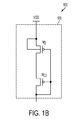
FIG. 1B is a schematic drawing of an exemplary integrated circuit including a P-type cascode transistor.
FIG. 2A is a schematic drawing of an integrated circuit including a bias circuit.
FIG. 2B is a schematic drawing of another exemplary integrated circuit including a bias circuit.
FIG. 3 is a schematic drawing of an exemplary operational amplifier.
FIG. 4 is a schematic drawing of an exemplary constant gm bias circuit.
FIG. 5 is a schematic drawing of an exemplary bandgap reference circuit.
DETAILED DESCRIPTION
In analog circuits, cascode technology is deployed to enhance electrical performances. In cascode technology, a cascode transistor is electrically coupled with a transistor in series. As the cascode transistor is operated as a diode having a low input resistance to the transistor, the voltage gain of the transistor becomes small, such that the bandwidth of the analog circuit is increased.
One cascode technique is to electrically connect a gate and a drain of the cascode transistor together. A gate and a drain of the transistor are electrically connected to each other. The gate of the cascode transistor is electrically isolated from the gate of the transistor. During the operation, the cascode transistor and the transistor are both operated in a saturation mode. In such a configuration, the supply voltage is designed to be larger than a sum of threshold voltages of the cascode transistor and the transistor. This configuration of the cascode transistor and the transistor makes the voltage headroom small.
Another cascode technique is to supply a bias voltage to the gate of the cascode transistor to enhance the voltage headroom. To provide a desired bias voltage, the bias circuit electrically coupled with the gate of the cascode transistor is complicated and may be difficult to design.
It is understood that the following disclosure provides many different embodiments, or examples, for implementing different features of various embodiments. Specific examples of components and arrangements are described below to simplify the present disclosure. These are, of course, merely examples and are not intended to be limiting. For example, the formation of a first feature over or on a second feature in the description that follows may include embodiments in which the first and second features are formed in direct contact, and may also include embodiments in which additional features may be formed between the first and second features, such that the first and second features may not be in direct contact. In addition, the present disclosure may repeat reference numerals and/or letters in the various examples. This repetition of reference numerals indicates the same element contained in different embodiments and does not in itself dictate a relationship between the various embodiments and/or configurations discussed.
FIG. 1A is a schematic drawing of an exemplary integrated circuit including an N-type cascode transistor. In FIG. 1A, an integrated circuit 100 includes an analog circuit 110. In some embodiments, the analog circuit 110 is an operational amplifier, a constant-gm bias circuit, a bandgap reference circuit, a current mirror, an analog to digital converter (ADC), a digital to analog converter (DAC), a pump circuit, a multiplexer, or one of other analog circuitries.
Referring to FIG. 1A, the analog circuit 110 includes a transistor M1. The transistor M1 is an N-type transistor as shown in FIG. 1A. The integrated circuit 100 includes at least one cascode transistor, e.g., cascode transistor MC1 that is electrically coupled with the transistor M1 in a series fashion. A drain and a gate of the cascode transistor MC1 are electrically coupled with a gate of the transistor M1 of the analog circuit 110. In some embodiments, a source and a bulk of the transistor M1 are electrically coupled with a bulk of the cascode transistor MC1 and electrically grounded.
During an operation, the cascode transistor MC1 is operated in a saturation mode or a sub-threshold mode. The transistor M1 is operated in a saturation mode. By operating the cascode transistor MC1 in a saturation mode or a sub-threshold mode, the voltage headroom between the drain of the cascode transistor MC1 and a supply voltage becomes larger. Additionally, the gates of the cascode transistor MC1 and the transistor M1 are electrically coupled with the drain of the cascode transistor MC1. No bias circuit is electrically coupled to a bulk of the cascode transistor MC1 and configured to provide a bias to adjust the operation mode of the cascode transistor MC1. As a result, the design of the integrated circuit 100 is simplified. The area that is assigned to accommodate the bias circuit is saved.
In some embodiments, the cascode transistor MC1 is operated in a sub-threshold mode, and the transistor M1 is operated in a saturation mode. To achieve the operation, the voltage differential (VGSC1) between the gate and the source of the cascode transistor MC1 is less than the threshold voltage (VTHC1) of the cascode transistor MC1. The threshold voltage (VTHC1) of the cascode transistor MC1 is less than the threshold voltage (VTH1) of the transistor M1. The relationship among the voltage differential VGSC1 and the threshold voltages VTHC1 and VTH1 can be shown as below:
VGSC1<VTHC1<VTH1
In some embodiments, the threshold voltage (VTHC1) of the cascode transistor MC1 being less than the threshold voltage (VTH1) of the transistor M1 allows a channel length of the cascode transistor MC1 to be designed shorter than a channel length of the transistor M1. In some embodiments, a channel width of the cascode transistor MC1 is designed to be wider than a channel width of the transistor M1. In other embodiments, the cascode transistor MC1 is a native transistor and the transistor M1 is not a native transistor. For example, the threshold voltage (VTHC1) of the cascode transistor MC1 is around 0, and the threshold voltage (VTH1) of the transistor M1 is higher than 0. In still other embodiments, the cascode transistor MC1 is a low threshold voltage (LVT) transistor or an ultra-low threshold voltage (ULVT) transistor. For example, the cascode transistor MC1 is an N-type LVT cascode transistor. The P-type dopant concentration in the channel region of the cascode transistor is lower than that of the transistor.
FIG. 1B is a schematic drawing of an exemplary integrated circuit including a P-type cascode transistor. In FIG. 1B, the integrated circuit 100 includes an analog circuit 120. In some embodiments, the analog circuit 120 is an operational amplifier, a constant-gm bias circuit, a bandgap reference circuit, a current mirror, an analog to digital converter (ADC), a digital to analog converter (DAC), a pump circuit, a multiplexer, or one of other analog circuitries.
Referring to FIG. 1B, the analog circuit 120 includes a transistor M2. The transistor M2 is a P-type transistor as shown in FIG. 1B. The integrated circuit 100 includes at least one cascode transistor, e.g., cascode transistor MC2 that is electrically coupled with the transistor M2 in a series fashion. The cascode transistor MC2 is a P-type cascode transistor. A drain and a gate of the cascode transistor MC2 are electrically coupled with a gate of the transistor M2 of the analog circuit 120. In some embodiments, a source and a bulk of the transistor M2 are electrically coupled to each other and with a supply voltage VDD.
As noted, the cascode transistor MC2 is operated in a saturation mode or a sub-threshold mode. The transistor M2 is operated in a saturation mode. By operating the cascode transistor MC2 in a saturation mode or a sub-threshold mode, the voltage headroom of the analog circuit 120 becomes larger. Additionally, the gates of the cascode transistor MC2 and the transistor M2 are electrically coupled with the drain of the cascode transistor MC2. No bias circuit is electrically coupled with and used to provide a bias to the bulk of the cascode transistor MC2 to adjust the operation mode of the cascode transistor MC2.
In some embodiments, the cascode transistor M
C2 is operated in a sub-threshold mode, and the transistor M
2 is operated in a saturation mode. To achieve the operation, the absolute value of the voltage differential (V
GSC2) between the gate and the source of the cascode transistor M
C2 is less than the absolute value of the threshold voltage (V
THC2) of the cascode transistor M
C2. The absolute value of the threshold voltage (V
THC2) of the cascode transistor M
C2 is less than the absolute value of the threshold voltage (C
TH2) of the transistor M
2. The relationship among the absolute values of the voltage differential V
GSC2 and the threshold voltages V
THC2 and V
TH2 is shown as below:
|V
⊥GSC2|<|V
⊥THC2|<|V
⊥TH2|
In some embodiments, the absolute value of the threshold voltage (VTHC2) of the cascode transistor MC2 being less than the absolute value of the threshold voltage (VTH2) of the transistor M2 allows a channel length of the cascode transistor MC2 to be designed shorter than a channel length of the transistor M2. In some embodiments, a channel width of the cascode transistor MC2 is designed to be wider than a channel width of the transistor M2. In some embodiments, the cascode transistor MC2 is a native transistor and the transistor M2 is not a native transistor. For example, the absolute value of the threshold voltage (VTHC2) of the cascode transistor MC2 is around 0, and the absolute value of the threshold voltage (VTH2) of the transistor M2 is higher than 0. In still some embodiments, the cascode transistor MC2 is a low threshold voltage (LVT) transistor or an ultra-low threshold voltage (ULVT) transistor. As noted, the cascode transistor MC2 is a P-type LVT transistor. The N-type dopant concentration in the channel region of the cascode transistor is lower than that of the transistor.
FIG. 2A is a schematic drawing of an integrated circuit including a bias circuit. In FIG. 2A, an integrated circuit 200 includes an analog circuit 210, which is the same as or similar to the analog circuit 110 described above in conjunction with FIG. 1A. In FIG. 2A, the analog circuit 210 includes a transistor M1 that is the same as or similar to the transistor M1 described above in conjunction with FIG. 1A. The integrated circuit 200 includes at least one cascode transistor, e.g., cascode transistor MC3 that is electrically coupled with the transistor M1 in a series fashion. A drain and a gate of the cascode transistor MC3 are electrically coupled with a gate of the transistor M1 of the analog circuit 210.
Referring to FIG. 2A, the integrated circuit 210 includes a bias circuit 230. The bias circuit 230 is electrically coupled with a bulk or a well region of the cascode transistor MC3. For example, the cascode transistor MC3 is an N-type cascode transistor. The bias circuit 230 is electrically coupled with a P-type well region or a P-type substrate of the cascode transistor MC3.
As noted, the cascode transistor MC3 is operated in a saturation mode or a sub-threshold mode. The transistor M1 is operated in a saturation mode. To achieve the operation, the threshold voltage (VTHC3) of the cascode transistor MC3 is lower than the threshold voltage (VTH1) of the cascode transistor M1.
In FIG. 2A, the bias circuit 230 is configured to lower the threshold voltage (VTHC3) of the cascode transistor MC3. For example, the transistor M1 and the cascode transistor MC3 are designed with the similar channel length, channel width, and/or dopant concentration. The bias circuit 230 is configured to provide a voltage to the P-type well region of the cascode transistor MC3, such that the threshold voltage (VTHC3) of the cascode transistor MC3 is lower than the threshold voltage (VTH1) of the cascode transistor M1.
In some embodiments, the bias circuit 230 includes transistors M3 and M4 that are electrically coupled to each other in a series fashion. The transistor M3 is an N-type transistor and the transistor M4 is a P-type transistor. A gate and a drain of the transistor M3 are electrically coupled with a node N1 between the transistors M3 and M4. The node N1 is electrically coupled with a bulk or a well region of the cascode transistor MC3. A bulk and a source of the transistor M4 are electrically coupled to each other and with a supply voltage VDD. A gate of the transistor M4 is controlled by a bias voltage that is provided from a bias circuit (not shown).
FIG. 2B is a schematic drawing of another exemplary integrated circuit including a bias circuit. In FIG. 2B, an integrated circuit 200 includes an analog circuit 220, which is the same as or similar to the analog circuit 120 described above in conjunction with FIG. 1B. In FIG. 2B, the analog circuit 220 includes a transistor M2 that is the same as or similar to the transistor M2 described above in conjunction with FIG. 1B. The integrated circuit 200 includes at least one cascode transistor, e.g., cascode transistor MC4 that is electrically coupled with the transistor M2 in a series fashion. A drain and a gate of the cascode transistor MC4 are electrically coupled with a gate of the transistor M2 of the analog circuit 220.
Referring to FIG. 2B, the integrated circuit 220 includes a bias circuit 240. The bias circuit 240 is electrically coupled with a well region of the cascode transistor MC4. For example, the cascode transistor MC4 is a P-type cascode transistor. The bias circuit 240 is electrically coupled with an N-type well region of the cascode transistor MC4.
As noted, the cascode transistor MC4 is operated in a saturation mode or a sub-threshold mode. The transistor M2 is operated in a saturation mode. It can be achieved by controlling the threshold voltage (VTHC4) of the cascode transistor MC4 lower than the threshold voltage (VTH2) of the cascode transistor M2.
In FIG. 2B, the bias circuit 240 is configured to lower the threshold voltage (VTHC4) of the cascode transistor MC4. For example, the transistor M2 and the cascode transistor MC4 have the similar channel length, channel width, and dopant concentration. The bias circuit 240 is configured to provide a voltage to the N-type well region of the cascode transistor MC4, such that the threshold voltage (VTHC4) of the cascode transistor MC4 is lower than the threshold voltage (VTH2) of the cascode transistor M2.
In some embodiments, the bias circuit 240 includes transistors M5 and M6 that are electrically coupled to each other in a series fashion. The transistors M5 and M6 are N-type transistors. A gate and a drain of the transistor M6 are electrically coupled to each other. A node N2 between the transistors M5 and M6 is electrically coupled with the N-type well region of the cascode transistor MC4. In some embodiments, a bulk and a source of the transistor M5 are electrically coupled with a bulk of the transistor M6. A gate of the transistor M5 is controlled by a bias voltage that is provided by a bias circuit (not shown).
Following are various exemplary analog circuits that include at least one cascode transistor described above in conjunction with FIGS. 1A-1B and 2A-2B. It is noted that the applications of the cascode technology of this application are not limited thereto. It is also noted that the configurations of the analog circuits below are merely exemplary. The scope of this application is not limited thereto.
FIG. 3 is a schematic drawing of an exemplary operational amplifier. In FIG. 3, an operational amplifier 300 includes transistors M301-M306 and cascode transistors MC301-MC306. The transistors M301 and M303 and the cascode transistors MC301 and MC303 are electrically coupled to each other in a series fashion between a current source and a supply voltage VDD. The transistors M302 and M304 and the cascode transistors MC302 and MC304 are electrically coupled to each other in a series fashion between the current source and the supply voltage VDD. The transistors M305 and M306 and the cascode transistors MC305 and MC306 are electrically coupled to each other in a series fashion. Gates of the transistors M301 and M302 of the operational amplifier 300 are configured to receive input signals. The operational amplifier 300 outputs at VOUT.
In some embodiments, gates of the cascode transistors MC301, MC302, and MC305 and the transistor M305 are electrically coupled with each other. Gates of the cascode transistors MC303, MC304, and MC306 and gates of the transistors M303, M304, and M306 are electrically coupled with each other. Bulks of the transistors M301 and M302 and the bulk of the cascode transistor MC302 are electrically coupled with the current source. Bulks of the transistors M303 and M304 are electrically coupled with the supply voltage VDD. A source and a bulk of the transistor M306 are electrically coupled with each other. A source and a bulk of the transistor M305 are electrically coupled with each other and electrically grounded.
Referring to FIG. 3, the configuration and operation of the transistors M301, M302 and M305 are the same as or similar to those of the transistor M1 described above in conjunction with FIG. 1A. The configuration and operation of the transistors M303, M304 and M306 are the same as or similar to those of the transistor M2 described above in conjunction with FIG. 1B. The configuration and operation of the cascode transistor MC305 are the same or similar to those of the cascode MC1 described above in conjunction with FIG. 1A. The configuration and operation of the cascode transistor MC304 are the same or similar to those of the cascode MC2 described above in conjunction with FIG. 1B.
In FIG. 3, configurations of the cascode transistors MC301 and MC302 are different from the cascode transistor MC305. For example, gates of the cascode transistors MC301 and MC302 are not electrically coupled with the gates of the transistors M301 and M302, respectively. The cascode transistors MC303 and MC306 are different from the cascode transistor MC304. For example, drains of the cascode transistors MC303 and MC306 are not electrically coupled with the gates of the cascode transistors MC303 and MC306, respectively. During the operation, the cascode transistors MC301, MC302, MC303 and MC306 are selectively operated in a saturation mode or a sub-threshold mode.
FIG. 4 is a schematic drawing of an exemplary constant gm bias circuit. In FIG. 4, a constant gm bias circuit 400 includes transistors M401-M404 and cascode transistors MC401-MC404. The transistors M401 and M403 and the cascode transistors MC401 and MC403 are electrically coupled to each other in a series fashion between ground and a supply voltage VDD. The transistors M402 and M404 and the cascode transistors MC402 and MC404 are electrically coupled to each other in a series fashion between a resistor R401 and the supply voltage VDD.
In some embodiments, gates of the cascode transistors MC401 and MC402 and gates of the transistors M401 and M402 are electrically coupled with each other. Gates of the cascode transistors MC403 and MC404 and gates of the transistors M403 and M404 are electrically coupled with each other. A bulk and a source of the transistor M401 are electrically coupled to each other and electrically grounded. A bulk and a source of the transistor M402 are electrically coupled to each other and with the resistor R401. Bulks of the transistors M403 and M404 are electrically coupled with the supply voltage VDD.
Referring to FIG. 4, the transistors M401 and M402 each are the same as or similar to the transistor M1 described above in conjunction with FIG. 1A. The transistors M403 and M404 each are the same as or similar to the transistor M2 described above in conjunction with FIG. 1B. The configuration and operation of the cascode transistors MC401 and MC402 are the same or similar to those of the cascode MC1 described above in conjunction with FIG. 1A. The configuration and operation of the cascode transistors MC403 and MC404 each are the same or similar to those of the cascode MC2 described above in conjunction with FIG. 1B.
FIG. 5 is a schematic drawing of an exemplary bandgap reference circuit. In FIG. 5, a bandgap reference circuit 500 includes transistors M501-M504, cascode transistors MC501-MC504, resistors R501-R503, and bipolar transistors B501-B502. The transistors M501 and M503, the cascode transistors MC501 and MC503, the resistor R502, and the bipolar transistor B502 are electrically coupled to each other in a series fashion between ground and a supply voltage VDD. The transistors M502 and M504, the cascode transistors MC502 and MC504, the resistors R501 and R503, and the bipolar transistor B501 are electrically coupled to each other in a series fashion between ground and the supply voltage VDD.
In some embodiments, gates of the cascode transistors MC501 and MC502 and gates of the transistors M501 and M502 are electrically coupled with each other. Gates of the cascode transistors MC503 and MC504 and gates of the transistors M503 and M504 are electrically coupled with each other. A bulk and a source of the transistor M501 are electrically coupled to each other and with the output VOUT of the bandgap reference circuit 500. A bulk and a source of the transistor M502 are electrically coupled to each other and with the resistor R503. Bulks of the transistors M503 and M504 are electrically coupled with the supply voltage VDD.
Referring to FIG. 5, the transistors M501 and M502 each are the same as or similar to the transistor M1 described above in conjunction with FIG. 1A. The transistors M503 and M504 each are the same as or similar to the transistor M2 described above in conjunction with FIG. 1B. The configuration and operation of the cascode transistors MC501 and MC502 are the same or similar to those of the cascode MC1 described above in conjunction with FIG. 1A. The configuration and operation of the cascode transistors MC503 and MC504 are the same or similar to those of the cascode MC2 described above in conjunction with FIG. 1B.
As noted, the descriptions of the analog circuits in conjunction with FIGS. 3-5 are merely exemplary. In some embodiments, the bias circuits 230 and 240 described above in conjunction with FIGS. 2A and 2B are selectively adapted to control the threshold voltages of the cascode transistors described above in conjunction with FIGS. 3-5.
One aspect of this description relates to an integrated circuit including a first circuit. The first circuit includes a first transistor having a first dopant type. The first circuit further includes a first cascode transistor having the first dopant type, wherein the first cascode transistor connected in series with the first transistor. The first circuit further includes a second transistor having a second dopant type opposite to the first dopant type, wherein the second transistor is connected in series with the first transistor. The first circuit includes a second cascode transistor having the second dopant type, wherein the second cascode transistor is connected in series with the second transistor. The integrated circuit further includes a first bias circuit configured to adjust a threshold voltage of at least one of the first cascode transistor or the second cascode transistor.
Another aspect of this description relates to an integrated circuit including a first circuit. The first circuit includes a first transistor having a first dopant type. The first circuit further includes a first cascode transistor having the first dopant type, wherein the first cascode transistor connected in series with the first transistor. The first circuit further includes a second transistor having a second dopant type opposite to the first dopant type, wherein the second transistor is connected in series with the first transistor. The first circuit includes a second cascode transistor having the second dopant type, wherein the second cascode transistor is connected in series with the second transistor. The integrated circuit further includes a first bias circuit configured to adjust a threshold voltage the first cascode transistor. The first bias circuit includes a first bias transistor having the second dopant type. The first bias circuit further includes a second bias transistor having the second dopant type, wherein the second bias transistor is connected in series with the first bias transistor, and a node between the first bias transistor and the second bias transistor is connected to a bulk of the first cascode transistor.
Still another aspect of this description relates to an integrated circuit. The integrated circuit includes a first circuit. The first circuit includes a first transistor having a first dopant type. The first circuit further includes a first cascode transistor having the first dopant type, wherein the first cascode transistor connected in series with the first transistor, and a gate of the first cascode transistor is connected to a gate of the first transistor. The first circuit further includes a second transistor having a second dopant type opposite to the first dopant type, wherein the second transistor is connected in series with the first transistor. The first circuit further includes a second cascode transistor having the second dopant type, wherein the second cascode transistor is connected in series with the second transistor, and a gate of the second cascode transistor is connected to a gate of the second transistor. The integrated circuit further includes a first bias circuit configured to adjust a threshold voltage the first cascode transistor. The first bias circuit includes a first bias transistor having the second dopant type. The first bias circuit further includes a second bias transistor having the second dopant type, wherein the second bias transistor is connected in series with the first bias transistor, and a node between the first bias transistor and the second bias transistor is connected to a bulk of the first cascode transistor.
The foregoing has outlined features of several embodiments so that those skilled in the art may better understand the detailed description. Those skilled in the art should appreciate that they may readily use the present disclosure as a basis for designing or modifying other processes and structures for carrying out the same purposes and/or achieving the same advantages of the embodiments introduced herein. Those skilled in the art should also realize that such equivalent constructions do not depart from the spirit and scope of the present disclosure, and that they may make various changes, substitutions and alterations herein without departing from the spirit and scope of the present disclosure.