US9159710B2 - Structures and methods for electrically and mechanically linked monolithically integrated transistor and NEMS/MEMS device - Google Patents
Structures and methods for electrically and mechanically linked monolithically integrated transistor and NEMS/MEMS device Download PDFInfo
- Publication number
- US9159710B2 US9159710B2 US13/990,830 US201113990830A US9159710B2 US 9159710 B2 US9159710 B2 US 9159710B2 US 201113990830 A US201113990830 A US 201113990830A US 9159710 B2 US9159710 B2 US 9159710B2
- Authority
- US
- United States
- Prior art keywords
- jfet
- nems
- semiconductor layer
- mems
- region
- Prior art date
- Legal status (The legal status is an assumption and is not a legal conclusion. Google has not performed a legal analysis and makes no representation as to the accuracy of the status listed.)
- Active
Links
- 101100460147 Sarcophaga bullata NEMS gene Proteins 0.000 title claims abstract description 121
- 238000000034 method Methods 0.000 title claims description 34
- 229910020968 MoSi2 Inorganic materials 0.000 claims abstract description 9
- 239000004065 semiconductor Substances 0.000 claims description 73
- VYPSYNLAJGMNEJ-UHFFFAOYSA-N Silicium dioxide Chemical compound O=[Si]=O VYPSYNLAJGMNEJ-UHFFFAOYSA-N 0.000 claims description 36
- 239000012212 insulator Substances 0.000 claims description 21
- 238000004519 manufacturing process Methods 0.000 claims description 21
- 229910052751 metal Inorganic materials 0.000 claims description 19
- 239000002184 metal Substances 0.000 claims description 19
- 239000000377 silicon dioxide Substances 0.000 claims description 18
- 239000000758 substrate Substances 0.000 claims description 17
- 229910052710 silicon Inorganic materials 0.000 claims description 11
- 239000010703 silicon Substances 0.000 claims description 11
- 235000012239 silicon dioxide Nutrition 0.000 claims description 10
- 238000007667 floating Methods 0.000 claims description 8
- 238000009792 diffusion process Methods 0.000 claims description 7
- 239000007787 solid Substances 0.000 claims description 4
- 238000000059 patterning Methods 0.000 claims 1
- 229910021332 silicide Inorganic materials 0.000 claims 1
- FVBUAEGBCNSCDD-UHFFFAOYSA-N silicide(4-) Chemical compound [Si-4] FVBUAEGBCNSCDD-UHFFFAOYSA-N 0.000 claims 1
- 230000010354 integration Effects 0.000 abstract description 18
- 230000003071 parasitic effect Effects 0.000 abstract description 11
- 238000012545 processing Methods 0.000 abstract description 6
- 238000001465 metallisation Methods 0.000 abstract description 2
- 230000019491 signal transduction Effects 0.000 abstract description 2
- 230000008569 process Effects 0.000 description 16
- 239000008186 active pharmaceutical agent Substances 0.000 description 12
- 229910052681 coesite Inorganic materials 0.000 description 12
- 229910052906 cristobalite Inorganic materials 0.000 description 12
- 229910052682 stishovite Inorganic materials 0.000 description 12
- 229910052905 tridymite Inorganic materials 0.000 description 12
- XUIMIQQOPSSXEZ-UHFFFAOYSA-N Silicon Chemical compound [Si] XUIMIQQOPSSXEZ-UHFFFAOYSA-N 0.000 description 9
- 239000002019 doping agent Substances 0.000 description 9
- 238000005516 engineering process Methods 0.000 description 8
- 230000005669 field effect Effects 0.000 description 8
- 235000012431 wafers Nutrition 0.000 description 6
- 230000008859 change Effects 0.000 description 5
- 239000004020 conductor Substances 0.000 description 5
- 238000000708 deep reactive-ion etching Methods 0.000 description 5
- 239000011651 chromium Substances 0.000 description 4
- 230000003750 conditioning effect Effects 0.000 description 4
- 238000006073 displacement reaction Methods 0.000 description 4
- 238000010237 hybrid technique Methods 0.000 description 4
- 239000000523 sample Substances 0.000 description 4
- 230000008878 coupling Effects 0.000 description 3
- 238000010168 coupling process Methods 0.000 description 3
- 238000005859 coupling reaction Methods 0.000 description 3
- 238000005530 etching Methods 0.000 description 3
- 230000006870 function Effects 0.000 description 3
- 150000002500 ions Chemical class 0.000 description 3
- 238000005259 measurement Methods 0.000 description 3
- 229910044991 metal oxide Inorganic materials 0.000 description 3
- 150000004706 metal oxides Chemical class 0.000 description 3
- 229920002120 photoresistant polymer Polymers 0.000 description 3
- 238000001020 plasma etching Methods 0.000 description 3
- 238000001039 wet etching Methods 0.000 description 3
- 230000001133 acceleration Effects 0.000 description 2
- 238000000137 annealing Methods 0.000 description 2
- 238000000231 atomic layer deposition Methods 0.000 description 2
- 238000000151 deposition Methods 0.000 description 2
- 230000008021 deposition Effects 0.000 description 2
- 238000001514 detection method Methods 0.000 description 2
- 230000000694 effects Effects 0.000 description 2
- 230000005684 electric field Effects 0.000 description 2
- 238000002955 isolation Methods 0.000 description 2
- 210000003127 knee Anatomy 0.000 description 2
- 239000000463 material Substances 0.000 description 2
- 230000003287 optical effect Effects 0.000 description 2
- 238000004806 packaging method and process Methods 0.000 description 2
- 238000000623 plasma-assisted chemical vapour deposition Methods 0.000 description 2
- BASFCYQUMIYNBI-UHFFFAOYSA-N platinum Chemical compound [Pt] BASFCYQUMIYNBI-UHFFFAOYSA-N 0.000 description 2
- 229920003229 poly(methyl methacrylate) Polymers 0.000 description 2
- 239000004926 polymethyl methacrylate Substances 0.000 description 2
- 238000011160 research Methods 0.000 description 2
- 230000004044 response Effects 0.000 description 2
- TVZRAEYQIKYCPH-UHFFFAOYSA-N 3-(trimethylsilyl)propane-1-sulfonic acid Chemical compound C[Si](C)(C)CCCS(O)(=O)=O TVZRAEYQIKYCPH-UHFFFAOYSA-N 0.000 description 1
- ZOXJGFHDIHLPTG-UHFFFAOYSA-N Boron Chemical compound [B] ZOXJGFHDIHLPTG-UHFFFAOYSA-N 0.000 description 1
- VYZAMTAEIAYCRO-UHFFFAOYSA-N Chromium Chemical compound [Cr] VYZAMTAEIAYCRO-UHFFFAOYSA-N 0.000 description 1
- 241001233242 Lontra Species 0.000 description 1
- ZOKXTWBITQBERF-UHFFFAOYSA-N Molybdenum Chemical compound [Mo] ZOKXTWBITQBERF-UHFFFAOYSA-N 0.000 description 1
- OAICVXFJPJFONN-UHFFFAOYSA-N Phosphorus Chemical compound [P] OAICVXFJPJFONN-UHFFFAOYSA-N 0.000 description 1
- 230000008901 benefit Effects 0.000 description 1
- 229910052796 boron Inorganic materials 0.000 description 1
- 239000000969 carrier Substances 0.000 description 1
- 229910052804 chromium Inorganic materials 0.000 description 1
- 238000004891 communication Methods 0.000 description 1
- 230000000295 complement effect Effects 0.000 description 1
- 239000000470 constituent Substances 0.000 description 1
- 238000010276 construction Methods 0.000 description 1
- 238000011161 development Methods 0.000 description 1
- 239000003989 dielectric material Substances 0.000 description 1
- 238000007599 discharging Methods 0.000 description 1
- 238000000609 electron-beam lithography Methods 0.000 description 1
- BHEPBYXIRTUNPN-UHFFFAOYSA-N hydridophosphorus(.) (triplet) Chemical compound [PH] BHEPBYXIRTUNPN-UHFFFAOYSA-N 0.000 description 1
- 238000002513 implantation Methods 0.000 description 1
- 238000001459 lithography Methods 0.000 description 1
- 150000002739 metals Chemical class 0.000 description 1
- 229910052750 molybdenum Inorganic materials 0.000 description 1
- 239000011733 molybdenum Substances 0.000 description 1
- NKAAEMMYHLFEFN-UHFFFAOYSA-M monosodium tartrate Chemical compound [Na+].OC(=O)C(O)C(O)C([O-])=O NKAAEMMYHLFEFN-UHFFFAOYSA-M 0.000 description 1
- 238000005457 optimization Methods 0.000 description 1
- 229910052698 phosphorus Inorganic materials 0.000 description 1
- 239000011574 phosphorus Substances 0.000 description 1
- 238000000206 photolithography Methods 0.000 description 1
- 229910052697 platinum Inorganic materials 0.000 description 1
- 238000012805 post-processing Methods 0.000 description 1
- 229920006395 saturated elastomer Polymers 0.000 description 1
- 229910000679 solder Inorganic materials 0.000 description 1
- 238000009987 spinning Methods 0.000 description 1
- 238000003860 storage Methods 0.000 description 1
- 238000000352 supercritical drying Methods 0.000 description 1
- 238000012546 transfer Methods 0.000 description 1
- LENZDBCJOHFCAS-UHFFFAOYSA-N tris Chemical compound OCC(N)(CO)CO LENZDBCJOHFCAS-UHFFFAOYSA-N 0.000 description 1
Images


Classifications
-
- H—ELECTRICITY
- H01—ELECTRIC ELEMENTS
- H01L—SEMICONDUCTOR DEVICES NOT COVERED BY CLASS H10
- H01L25/00—Assemblies consisting of a plurality of individual semiconductor or other solid state devices ; Multistep manufacturing processes thereof
- H01L25/16—Assemblies consisting of a plurality of individual semiconductor or other solid state devices ; Multistep manufacturing processes thereof the devices being of types provided for in two or more different main groups of groups H01L27/00 - H01L33/00, or in a single subclass of H10K, H10N, e.g. forming hybrid circuits
-
- B—PERFORMING OPERATIONS; TRANSPORTING
- B81—MICROSTRUCTURAL TECHNOLOGY
- B81C—PROCESSES OR APPARATUS SPECIALLY ADAPTED FOR THE MANUFACTURE OR TREATMENT OF MICROSTRUCTURAL DEVICES OR SYSTEMS
- B81C1/00—Manufacture or treatment of devices or systems in or on a substrate
- B81C1/00015—Manufacture or treatment of devices or systems in or on a substrate for manufacturing microsystems
- B81C1/00222—Integrating an electronic processing unit with a micromechanical structure
- B81C1/00246—Monolithic integration, i.e. micromechanical structure and electronic processing unit are integrated on the same substrate
-
- H—ELECTRICITY
- H01—ELECTRIC ELEMENTS
- H01L—SEMICONDUCTOR DEVICES NOT COVERED BY CLASS H10
- H01L29/00—Semiconductor devices adapted for rectifying, amplifying, oscillating or switching, or capacitors or resistors with at least one potential-jump barrier or surface barrier, e.g. PN junction depletion layer or carrier concentration layer; Details of semiconductor bodies or of electrodes thereof ; Multistep manufacturing processes therefor
- H01L29/40—Electrodes ; Multistep manufacturing processes therefor
- H01L29/41—Electrodes ; Multistep manufacturing processes therefor characterised by their shape, relative sizes or dispositions
- H01L29/423—Electrodes ; Multistep manufacturing processes therefor characterised by their shape, relative sizes or dispositions not carrying the current to be rectified, amplified or switched
- H01L29/42312—Gate electrodes for field effect devices
- H01L29/42316—Gate electrodes for field effect devices for field-effect transistors
-
- H—ELECTRICITY
- H01—ELECTRIC ELEMENTS
- H01L—SEMICONDUCTOR DEVICES NOT COVERED BY CLASS H10
- H01L29/00—Semiconductor devices adapted for rectifying, amplifying, oscillating or switching, or capacitors or resistors with at least one potential-jump barrier or surface barrier, e.g. PN junction depletion layer or carrier concentration layer; Details of semiconductor bodies or of electrodes thereof ; Multistep manufacturing processes therefor
- H01L29/66—Types of semiconductor device ; Multistep manufacturing processes therefor
- H01L29/66007—Multistep manufacturing processes
- H01L29/66075—Multistep manufacturing processes of devices having semiconductor bodies comprising group 14 or group 13/15 materials
- H01L29/66227—Multistep manufacturing processes of devices having semiconductor bodies comprising group 14 or group 13/15 materials the devices being controllable only by the electric current supplied or the electric potential applied, to an electrode which does not carry the current to be rectified, amplified or switched, e.g. three-terminal devices
- H01L29/66409—Unipolar field-effect transistors
- H01L29/66893—Unipolar field-effect transistors with a PN junction gate, i.e. JFET
- H01L29/66901—Unipolar field-effect transistors with a PN junction gate, i.e. JFET with a PN homojunction gate
-
- H—ELECTRICITY
- H01—ELECTRIC ELEMENTS
- H01L—SEMICONDUCTOR DEVICES NOT COVERED BY CLASS H10
- H01L29/00—Semiconductor devices adapted for rectifying, amplifying, oscillating or switching, or capacitors or resistors with at least one potential-jump barrier or surface barrier, e.g. PN junction depletion layer or carrier concentration layer; Details of semiconductor bodies or of electrodes thereof ; Multistep manufacturing processes therefor
- H01L29/66—Types of semiconductor device ; Multistep manufacturing processes therefor
- H01L29/68—Types of semiconductor device ; Multistep manufacturing processes therefor controllable by only the electric current supplied, or only the electric potential applied, to an electrode which does not carry the current to be rectified, amplified or switched
- H01L29/70—Bipolar devices
- H01L29/72—Transistor-type devices, i.e. able to continuously respond to applied control signals
- H01L29/73—Bipolar junction transistors
- H01L29/735—Lateral transistors
-
- H—ELECTRICITY
- H01—ELECTRIC ELEMENTS
- H01L—SEMICONDUCTOR DEVICES NOT COVERED BY CLASS H10
- H01L29/00—Semiconductor devices adapted for rectifying, amplifying, oscillating or switching, or capacitors or resistors with at least one potential-jump barrier or surface barrier, e.g. PN junction depletion layer or carrier concentration layer; Details of semiconductor bodies or of electrodes thereof ; Multistep manufacturing processes therefor
- H01L29/66—Types of semiconductor device ; Multistep manufacturing processes therefor
- H01L29/68—Types of semiconductor device ; Multistep manufacturing processes therefor controllable by only the electric current supplied, or only the electric potential applied, to an electrode which does not carry the current to be rectified, amplified or switched
- H01L29/76—Unipolar devices, e.g. field effect transistors
- H01L29/772—Field effect transistors
- H01L29/80—Field effect transistors with field effect produced by a PN or other rectifying junction gate, i.e. potential-jump barrier
- H01L29/808—Field effect transistors with field effect produced by a PN or other rectifying junction gate, i.e. potential-jump barrier with a PN junction gate, e.g. PN homojunction gate
- H01L29/8086—Thin film JFET's
-
- H—ELECTRICITY
- H01—ELECTRIC ELEMENTS
- H01L—SEMICONDUCTOR DEVICES NOT COVERED BY CLASS H10
- H01L29/00—Semiconductor devices adapted for rectifying, amplifying, oscillating or switching, or capacitors or resistors with at least one potential-jump barrier or surface barrier, e.g. PN junction depletion layer or carrier concentration layer; Details of semiconductor bodies or of electrodes thereof ; Multistep manufacturing processes therefor
- H01L29/66—Types of semiconductor device ; Multistep manufacturing processes therefor
- H01L29/68—Types of semiconductor device ; Multistep manufacturing processes therefor controllable by only the electric current supplied, or only the electric potential applied, to an electrode which does not carry the current to be rectified, amplified or switched
- H01L29/76—Unipolar devices, e.g. field effect transistors
- H01L29/772—Field effect transistors
- H01L29/80—Field effect transistors with field effect produced by a PN or other rectifying junction gate, i.e. potential-jump barrier
- H01L29/812—Field effect transistors with field effect produced by a PN or other rectifying junction gate, i.e. potential-jump barrier with a Schottky gate
- H01L29/8126—Thin film MESFET's
-
- B—PERFORMING OPERATIONS; TRANSPORTING
- B81—MICROSTRUCTURAL TECHNOLOGY
- B81C—PROCESSES OR APPARATUS SPECIALLY ADAPTED FOR THE MANUFACTURE OR TREATMENT OF MICROSTRUCTURAL DEVICES OR SYSTEMS
- B81C2203/00—Forming microstructural systems
- B81C2203/07—Integrating an electronic processing unit with a micromechanical structure
- B81C2203/0707—Monolithic integration, i.e. the electronic processing unit is formed on or in the same substrate as the micromechanical structure
- B81C2203/075—Monolithic integration, i.e. the electronic processing unit is formed on or in the same substrate as the micromechanical structure the electronic processing unit being integrated into an element of the micromechanical structure
-
- H—ELECTRICITY
- H01—ELECTRIC ELEMENTS
- H01L—SEMICONDUCTOR DEVICES NOT COVERED BY CLASS H10
- H01L2924/00—Indexing scheme for arrangements or methods for connecting or disconnecting semiconductor or solid-state bodies as covered by H01L24/00
-
- H—ELECTRICITY
- H01—ELECTRIC ELEMENTS
- H01L—SEMICONDUCTOR DEVICES NOT COVERED BY CLASS H10
- H01L2924/00—Indexing scheme for arrangements or methods for connecting or disconnecting semiconductor or solid-state bodies as covered by H01L24/00
- H01L2924/0001—Technical content checked by a classifier
- H01L2924/0002—Not covered by any one of groups H01L24/00, H01L24/00 and H01L2224/00
Definitions
- the present invention relates to JFETs, and especially JFETS designed to be suitable for use in helping to control NEMS/MEMS scale machines (herein called “NEMS/MEMS machines,” see also, “NEMS/MEMS scale” in the DEFINITIONS section).
- the present invention further relates to devices which include both the NEMS/MEMS machine and at least some of the circuitry for controlling the operation of the NEMS/MEMS machine (see definition section).
- NEMS/MEMS machines see also, “NEMS/MEMS scale” in the DEFINITIONS section.
- the present invention further relates to devices which include both the NEMS/MEMS machine and at least some of the circuitry for controlling the operation of the NEMS/MEMS machine (see definition section).
- These combinations of the NEMS/MEMS machine hardware set and at least a portion of its control circuitry e.g. a JFET
- NEMS/MEMS devices will sometimes herein be referred to as “NEMS/MEMS devices.”
- conventional SOI-NEMS/MEMS device includes: An electronics chip consisting mostly of complementary metal oxide (“CMOS”) semiconductor transistors, but active electronic transistors in general, 102 ; bonded conduction path 112 ; and NEMS/MEMS chip 113 .
- Electronics chip 102 includes: contact pad/s 104 , 110 ; demodulator/filter/pre-amp/reference module 106 ; and amplifier 108 .
- NEMS/MEMS chip 113 includes: mechanical springs and masses 114 ; fingers often used for electrostatic actuation 116 ; anchor 118 ; proof mass 119 ; and contact pads 120 .
- Sub-assembly 114 moves in the directions indicated by arrows D1 and D2: (i) to create an electrical signal; and/or (ii) in response to an electrical signal.
- This sort of conventional NEMS/MEMS device is part of many commercial products and/or proposed products, such as accelerometers, gyroscopes, electrical switches, resonators, timing devices, optical switches, optical gratings, and microfluidic devices.
- Many commercial NEMS/MEMS devices are made with thicker suspended parts to obtain higher mass and greater sense capacitances. This has been obtained through using SOI wafers and etching them using DRIE processing techniques. Even without SOI substrates, using processes such as SCREAM, high aspect ratio NEMS/MEMS devices are commercially available.
- a NEMS/MEMS device including a NEMS/MEMS machine and an associated transistor in the form of a JFET, is disclosed in U.S. Pat. No. 7,205,173 (“Brunson”).
- Brunson the JFET portions of the NEMS/MEMS device are in the form of “wells,” which is to say that the doping that creates the constituent regions of the Brunson JFET is accomplished by diffusing dopants into the wafer thickness (that is, in a direction substantially normal to the major surface of the semiconductor layer through which the diffusion occurs.
- the doped wells forming the Brunson JFET do not extend all the way across the thickness of their semiconductor layer (that is, the wells do not extend from one major surface of the semiconductor, all the way to the opposite major surface. Because of the geometry of the well structures in Brunson, the channel conductance is squeezed (and sometimes pinched off) by depleted zone(s) that expand in the thickness direction of the semiconductor layer to control conduction.
- NEMS/MEMS were integrated with the JFET transistors monolithically, but the link between transistors and the NEMS/MEMS was purely electrical. The output of the NEMS/MEMS, being capacitive output, was linked to the transistor gates.
- the present invention recognizes that in hybrid architecture device 100 , the wire bond introduces parasitic phenomena as well as mismatch phenomena.
- the present invention further recognizes that monolithic integration of NEMS/MEMS machines, with FETs, results in the minimization of the wire-bond parasitic phenomena, and that this minimization of parasitics can be highly advantageous.
- the hybrid solution introduces parasitics and mismatches during the assembly and packaging of the FETS and NEMS components due to the wire bonds that connects the two dice and this prevents SOI-NEMS/MEMS to fully realize optimal performance.
- One aspect of the present invention is directed to a JFET structure (and associated methods of making and/or using) that is contained and insulated within a single semiconductor layer in a monolithically integrated chip stack.
- Another aspect of the present invention is a NEMS/MEMS device (and associated methods of making and/or using) that includes a NEMS/MEMS machine and a JFET structure that is contained and insulated within a single semiconductor layer in a monolithically integrated chip stack. In at least some JFETs according to the present invention.
- NEMS/MEMS devices are being constructed from high aspect ratio DRIE etched silicon, and the lateral beam thicknesses can be small, the JFET transistors can be integrated within beam structures used in NEMS/MEMS. Direct integration within the springs and masses used would lead to optimal use of chip-real-estate, and minimize interconnects to sensing elements.
- Using the thin lateral dimensions one can diffuse dopants into high aspect ratio beams laterally; and do define channel conduction to extend across the entire thickness of a silicon layer (bounded on at least its lower side by an insulative layer (e.g., a silicon dioxide layer). This is to be sharply distinguished from Brunson, where the well structures defining the channel only extend part way across the thickness of their semiconductor layer medium.
- the JFET By using a JFET without wells, and instead with doped regions that span the entire thickness of the semiconductor layer. the JFET becomes easier to make and/or has improved performance especially when tightly electrically integrated on a single chip with a NEMS/MEMS machine.
- the beams which are part of the NEMS/MEMS can, in some embodiments of the present invention, be released for tightly integrated transistor and NEMS/MEMS such that the transistors are directly part of the NEMS/MEMS.
- the JFET transistor(s) can be integrated within the material of the cantilever beam structures (and/or otter moving parts) used in NEMS/MEMS. Direct integration within the springs and masses used would lead to optimal use of chip-real-estate, and minimize interconnects to sensing elements.
- the thin lateral dimensions one can diffuse dopants into high aspect ratio beams laterally; do define channel conduction along the wafer, instead of vertically into the wafer as in traditional JFETs.
- the beams which are part of the NEMS/MEMS can be released for tightly integrated transistor and NEMS/MEMS such that the transistors are directly part of the NEMS/MEMS.
- a device includes: (a) a first insulator layer that defines: (i) the major plane of the device; and (ii) a transverse direction that is normal to the major plane at any given point on the major plane; and (b) a first semiconductor layer.
- the first semiconductor layer and the first insulator layer are monolithically integrated into a stack structure.
- the stack structure includes a first NEMS/MEMS region.
- the first NEMS/MEMS region of the stack structure is structured, connected, sized, shaped and/or located to operate as a first NEMS/MEMS machine that includes a first moving part.
- the semiconductor layer includes a first major surface and a second major surface, spaced apart in the transverse direction.
- the JFET structure includes a first insulator layer and a first semiconductor layer.
- the method includes the following steps: monolithically forming the first semiconductor layer and the first insulator layer into a stack structure so that the first semiconductor layer includes the JFET structure such that the JFET structure is electrically isolated from other layers of the stack structure; x doping the first semiconductor layer, across its entire transverse direction, to form in the first semiconductor layer a source region; x doping the first semiconductor layer, across its entire transverse direction, to form in the first semiconductor layer a drain region; lightly x doping the first semiconductor layer, across its entire transverse direction, to form in the first semiconductor layer a conductance channel; and y doping the first semiconductor layer, across its entire transverse direction, to form in the first semiconductor layer a first gate region.
- x is a first doping type (either p or n).
- y is a second doping type (either p or n).
- the doping steps create the JFET structure within the first semiconductor layer.
- the JFET structure is structured, located and/or connected so that during operation of the JFET structure: (i) the conductance channel of the first JFET structure will develop depleted and undepleted portions, and (ii) the depleted portions will, at times and as determined by operating conditions, expand to pinch off the conductance channel.
- FIG. 1 is a schematic view of a prior art NEMS/MEMS device
- FIG. 2 is a schematic view of a first embodiment of a NEMS/MEMS device according to the present invention
- FIG. 3A a plan view of a first embodiment of a JFET according to the present invention
- FIG. 3B a plan and cross-sectional view of the first embodiment JFET operating at its “knee voltage;”
- FIG. 3C a plan and cross-sectional view of the first embodiment JFET operating above its “knee voltage;”
- FIG. 3D is a graph showing certain characteristics of the performance of the first embodiment JFET
- FIG. 4 is schematic view of a second embodiment of a NEMS/MEMS device according to the present invention.
- FIG. 6A is another schematic view of the second embodiment NEMS/MEMS device
- FIG. 6B is an orthographic plan view of the second embodiment NEMS/MEMS device
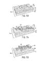
- FIGS. 7A to 7O is a cross-sectional view that shows the layered structure of a third embodiment of a NEMS/MEMS device according to the present invention as it is being monolithically integrated and otherwise manufactured;
- FIG. 8 is a schematic view of a fourth embodiment of a NEMS/MEMS device according to the present invention.
- FIG. 9 is a graph showing certain characteristics of the performance of the fourth embodiment NEMS/MEMS device.
- FIG. 10 is a schematic view of a fifth embodiment of a NEMS/MEMS device according to the present invention.
- FIG. 11 is a graph showing certain characteristics of the performance of the fifth embodiment NEMS/MEMS device.
- FIG. 12 is a schematic view, of a sixth embodiment of a NEMS/MEMS device according to the present invention.
- FIG. 13 is a graph showing certain characteristics of the performance of the sixth embodiment NEMS/MEMS device.
- FIG. 14 is a schematic view of a seventh embodiment of a NEMS/MEMS device according to the present invention.
- FIG. 15 is a graph showing certain characteristics of the performance of the seventh embodiment NEMS/MEMS device.
- FIG. 16 is a graph showing certain characteristics of the performance of various embodiments of NEMS/MEMS devices according to the present invention.
- FIG. 17A is a perspective view of a circuit according to the present invention.
- FIG. 17B is another perspective view of the FIG. 17A circuit
- FIG. 18 is a perspective view of another circuit according to the present invention.
- FIG. 19 is a plan view of an eighth embodiment of a NEMS/MEMS device according to the present invention.
- FIG. 20 is a perspective view of the eighth embodiment device.
- FIG. 21 is a graph showing certain characteristics of the performance of a NEMS/MEMS device according to the present invention.
- FIG. 22 is a graph showing certain characteristics of the performance of a NEMS/MEMS device according to the present invention.
- FIG. 23 shows a transverse cross-section of a three layer SOI stack suitable for use in various embodiments of the present invention.
- FIG. 24 shows a first alternative NEMS/MEMS system level architecture (including certain control electronics, other than the JFET sensor/amplifiers, which will herein be sometimes referred to as CMOS control electronics);
- FIG. 25 shows a second alternative of CMOS and NEMS/MEMS system level architecture (including certain control electronics, other than the JFET sensor/amplifiers, which will herein be sometimes referred to as CMOS control electronics);
- FIG. 26 shows a third alternative of CMOS and NEMS/MEMS system level architecture (including certain control electronics, other than the JFET sensor/amplifiers, which will herein be sometimes referred to as CMOS control electronics);
- FIG. 27 is a perspective view of a device 825 according to the present invention, the device including source 826 , gate 827 and drain 828 .
- FIG. 28 is a method of fabricating with nine intermediate stack structures that exist during the manufacturing process.
- FIG. 29 is a method of fabricating showing eleven intermediate stack structures that exist during the manufacturing process.
- FIG. 2 shows a NEMS/MEMS device 200 , which is substantially constituted by a single, monolithically integrated chip 202 .
- the NEMS/MEMS device may include additional control electronics, such as a processing network, located on a second chip substrate.
- the NEMS/MEMS machine and at least one of its associated transistors are located on the single chip 202 .
- chip 202 includes: first terminal T 1 ; demodulator/filters/pre-amp/reference module 206 ; amplifier 208 ; non-bonded path 212 ; anchor structures 218 ; spring/mass sub-assembly 214 ; proof mass 219 ; and finger structure 216 .
- JFET 250 includes: drain region 252 ; first gate region 254 ; source region 256 ; second gate region 258 and channel region 251 .
- channel region 251 connects source 256 to drain 252 .
- channel region 251 includes: first semiconductor layer 261 ; insulator layer 280 (made of, e.g., silicon dioxide); and second semiconductor layer 282 (made of, e.g., silicon).
- first semiconductor layer 261 a semiconductor layer 261 ; insulator layer 280 (made of, e.g., silicon dioxide); and second semiconductor layer 282 (made of, e.g., silicon).
- first semiconductor layer 261 includes: first p doped sub-region 260 ; second p doped sub-region 270 ; first carrier-depleted channel portion 262 of lightly n doped region 262 , 264 , 266 ; second carrier-depleted channel portion 266 of lightly n doped region 262 , 264 , 266 ; and carrier-undepleted channel portion 264 of lightly n doped region 262 , 264 , 266 .
- the channel sub-region in layer 261 therefore includes depleted portions 262 and 266 , as well as undepleted portion 264 .
- This channel sub-region 262 , 264 , 266 is lightly n doped. As can be seen by comparing FIG.
- the width of the carrier depleted zone increases in footprint when the electrical potential between the drain and source increases.
- the carrier depleted portions 262 , 266 will swell to the extent that they “pinch off” the undepleted portion such that the undepleted portion no longer extends continuously from the drain to the source.
- graph 299 of FIG. 3D once this phenomenon of pinch off occurs, then further increases in the magnitude of the electrical potential between the source and drain will not result in an increase of current flow through the channel sub-region 262 , 264 , 266 .
- An n-channel JFET is a majority carrier transistor where: (i) electrons flow from the source toward the drain; and (ii) holes flow from the drain toward the source.
- FIGS. 3B and 3C each show the top view and the transverse cross-section of a channel region in 4-terminal n-channel JFET 250 , with 3 B and 3 C respectively showing the JFET in: (i) an unsaturated state (although getting close to saturation); and (ii) a saturated state.
- a comparison of FIGS. 3B and 3C show the gradual increase in the width of depleted portions 262 and 266 as V DS is increased.
- the source, gate-1 and gate-2 are tied to ground.
- the channel acts like an ohmic resistor (see region I of FIG. 3D ) and current flows from the drain to the source.
- V DS increases, the reverse bias on the pn-junction between the drain and the gate is further reverse biased. Because of this reverse bias, depleted portions 262 , 266 form between the gates (more precisely, the p doped sub-regions in the channel region) and the undepleted portion of lightly n doped sub-region 262 , 264 , 266 when V DS is present.
- I D ⁇ ( sat ) I DSS ⁇ ( 1 - ( V GS V P ) ) 2 ( 1 )
- F 1 1 2 ⁇ ⁇ 0 ⁇ A ( d - x ) 2 ⁇ ( V G ⁇ ⁇ 3 - V G ⁇ ⁇ 2 ) 2 ( 2 )
- F 2 - 1 2 ⁇ ⁇ 0 ⁇ A ( d + x ) 2 ⁇ ( V G ⁇ ⁇ 2 ) 2 ( 3 )
- ⁇ 0 is the permittivity of vacuum
- x is the beam displacement.
- x F + F 3 k ( 6 )
- V G ⁇ ⁇ 2 ( C nems ⁇ ⁇ 1 C nems ⁇ ⁇ 1 + C dep // C nems ⁇ ⁇ 2 ) ⁇ V G ⁇ ⁇ 3 ( 7 )
- C nems1 is the capacitance between the gate-3 and cantilever
- C nems2 is the capacitance between the cantilever and gate-4
- C dep is the depletion capacitance at the
- C dep ( q ⁇ ⁇ ⁇ si ⁇ N d 2 ⁇ ( V bi - V G ⁇ ⁇ 2 ) ) ⁇ A ( 10 )
- V G2 can be determined numerically by substituting Eq. 8, 9 and 10 into Eq. 7.
- Equation (1) shows a useful approximation of the saturation current for JFETS like JFET 250 .
- V Gs 0V
- V P is the pinch-off voltage.
- NEMS/MEMS device 300 including: JFET 250 ; and NEMS/MEMS machine 312 (including moveable cantilever member 312 a , first stationary member 312 b and second stationary member 312 c ).
- JFET 250 includes a channel region which includes the following sub-regions: drain interface sub-region 302 ; first and second p doped sub-regions 306 , 308 ; source interface sub-region 304 ; and lightly n doped sub-region 303 , 305 , 310 (including undepleted portion 310 , and, when applicable, depleted zones 303 , 305 that can change in their size and shape depending upon operating conditions).
- this detection of the cantilever position is provided to the second p doped sub-region 308 of the channel region of JFET 250 in an extremely direct way because the cantilever member extends directly from, and is monolithically integrated with, the second p doped sub-region. In this way, changes in the cantilever member position in space will cause corresponding changes to channel conductance of JFET 250 , and cantilever position helps control the operation of JFET 250 through this control of channel conductance.
- the conducting channel (including both its depleted and undepleted portions) is lightly n-type doped.
- the gates interface sub-regions 306 and 308 are p+ doped and the source and drain interface sub-regions 302 and 304 are n+ doped.
- cantilever member 312 a is 250 nm wide and is surrounded by stationary members 312 b and 312 c (sometimes respectively denominated herein as gate 3 and gate 4).
- the bulk is the substrate of the SOI wafer. Additional mechanical components such as beam stoppers can be used to limit motion. These stopper enables the NEMS/MEMS machine to be configured into an electrical switch.
- FIGS. 6A and B respectively are: (i) the equivalent capacitive model; and a plan view of the JFET-NEMS device.
- Equation (3) ⁇ 0 is the permittivity of vacuum
- x is the beam displacement.
- Equation (4) F3 is a parasitic force which is a negative spring and is known as spring softening.
- the electrostatic force is equal to the spring force as in Equation (5), above.
- Equation (5) m is the mass
- g is the acceleration
- Equation (7) the floating potential V G2 of the cantilever is given by Equation (7), above.
- Equation (7) C nems1 and C nems2 are derived as Equations (8) and (9), above. Equation (6) can be substituted into Equations (8) and (9).
- V G2 can be determined numerically by substituting Equations (8), (9) and (10) into Equation (7).
- Stacks-in-progress 500 a to 500 o collectively include the following layers: first silicon layer 502 ; first silicon dioxide (or insulator) layer 504 ; second silicon layer 506 ; second silicon dioxide (or insulator) layer 508 ; first chromium layer 510 ; first resist layer 512 ; n doped portion 514 ; p doped portion 518 ; metal line layer 520 ; third silicon dioxide layer 522 ; second resist layer 524 .
- 7A to 7O are as follows: ( 7 A) SOI substrate provided; ( 7 B) SiO 2 and Cr deposition; ( 7 C) Polymethyl methacrylate (“PMMA”) resist spinning; (D) Ebeam exposure of n+ region; (E) reactive-ion etching (“RIE”) of Cr and SiO 2 etching; (F) wet etching of resist and Cr; (G) solid source diffusion of phosphorous dopant and annealing; (H) wet etching of SiO 2 diffusion mask; (I) repeat steps shown in FIGS.
- PMMA Polymethyl methacrylate
- the contact electrodes were silicidated with metal, preferably MoSi 2 .
- MoSi 2 by its inherent material properties, has low resistance and exhibits low stress even as it moves with the moving part(s) of the NEMS/MEMS machine. This was done to ensure that there was ohmic contact between the Si and the probing pads.
- MoSi 2 (or other suitable metal) is sputtered and Rapid Thermal Annealed (RTA) at 750° C. in Ar gas for 3 minutes to form the ohmic contacts (including non-bonded conduction path(s) between each NEMS/MEMS machine and its associated JFET(s).
- RTA Rapid Thermal Annealed
- the fabrication process involved 4 levels of electron beam lithography and 5 levels of photolithography. The mask count could be drastically reduced to 4 if deep ultraviolet (“DUV”) lithography is used for the exposures of the NEMS components and the probing pads. We are currently using ASML DUV tool to make these devices.
- DUV deep ultraviolet
- FIG. 8 is a schematic 400 helpful in understanding graph 401 of FIG. 9 .
- Graph 401 is the plot of I D versus V DS and it shows saturation as the channel is pinched-off.
- Graph 401 shows measured I DS versus V DS output curves for a JFET-NEMS device. The measured low current is due to the high drain and source resistances.
- FIG. 10 is a schematic 600 helpful in understanding graph 601 of FIG. 11 .
- JFET-NEMS device A Common Source Amplifier Configuration of JFET-NEMS device will now be discussed.
- the JFET is then configured into a common source amplifier by connecting a 3 M ⁇ resistor at the drain.
- a 3 M ⁇ resistor is justified due to the very large input resistance of the transistor channel.
- the transconductance (gm) of the transistor was 13.3 ⁇ S. This value is low due to a large parasitic resistance formed at the source and drain terminals. This large resistance leads to a very large RC time constant for charging and discharging the load capacitances, leading to a low frequency operation of 351 Hz.
- An AC signal is input at gate 3 and the drain output connected to an oscilloscope. The AC signal couples into the cantilever and this signal is transduced through the JFET portion.
- FIG. 14 shows schematic 750 , which is helpful for understanding graph 751 .
- the capacitance from gate 3 to cantilever is 0.55 fF, and the capacitance from cantilever to gate of JFET is 0.53 fF.
- the 3M ⁇ resistor is removed and the drain voltage is swept from 0-3V.
- the source, gate 1 and gate 4 voltages are placed at 0V.
- the cantilever member has an electrical potential that floats in magnitude and/or direction as the body of the cantilever member moves through the electrical field created by the potential of the stationary members (see FIG. 4 ) that constitute gates 3 and 4.
- the phenomenon of capacitive coupling is what causes the cantilever member (that is, gate 2) to vary in voltage as it changes its position relative to stationary gates 3 and 4.
- V G2 This floating potential modulates the channel conductance.
- C nems1 increases and it results in the increase of V G2 .
- V G3 is negative
- V G2 is also negative according to Equation (7) and it reverse biases the cantilever-JFET junction.
- FIG. 16 shows graph 799 , which is the plot of the response of the JFET to the motion of a clamp-free cantilever and a clamp-clamp cantilever. Since the clamp-free cantilever has a higher displacement with the same gate 3 voltage, its V G2 is higher than the case of clamp-clamp beam and it is better able to modulate the drain channel conductance. As shown in FIG. 16 , the JFET-NEMS device is able to sense the motion with the clamp-free and a clamp-clamp cantilever as gate 3 voltage is applied. The change in current is much larger for the clamped-free case.
- the drain current modulation could be partly due to piezoresistive effect at the cantilever-channel junction that occurs as the beam bends.
- One feature of some embodiments of the present invention is monolithic integration of JFET with moving gates that can be NEMS or MEMS.
- the fabrication of the devices utilizes embedded JFET junctions at cross-points of SOI beams.
- Another feature of some embodiments of the present invention is that the JFET amplifier gain as well as its use in sensing a motion characteristic (e.g., position) of a moving part of a NEMS/MEMS machine.
- the moving part(s) of the NEMS/MEMS machine may (without limitation) take various forms, such as a cantilever, an inertial sensor, a resonator, switch(es).
- tightly coupled NEMS/MEMS and electronics reduce parasitics and improve performance. Because SOI beams are common to many MEMS devices, JFETs can be used to sense and amplify motion for increased signal and reduce effect of parasitic capacitances encountered in two-chip MEMS and NEMS.
- BJTs Bipolar Junction Transistors
- npn the doping concentration at the collector, base and emitter.
- pnp the doping concentration at the collector, base and emitter.
- Three implantations or solid diffusion has to be carried out. The first diffusion at the emitter, the second at the base and the third at the collector terminals. The emitter and the collector are dosed with the same dopant (n or p) but the doping concentration at the emitter is higher than at the collector. DRIE is used to define the junctions.
- FIGS. 17A and 17B show schematic 800 of the proposed BJT.
- BJT Bipolar Junction Transistor
- the emitter is highly doped than the collector.
- NPN and PNP transistors can be fabricated using this technology.
- B The cross section of a released device. The conducting channel for all these devices can be released by etching away the buried oxide. Releasing the conducting layer provides isolation and reduces parasitics between the channel and the substrate.
- MESFET Metal Semiconductor Field Effect Transistor
- JFET Metal Semiconductor Field Effect Transistor
- the device is unipolar and majority carrier conducts the current through the channel.
- the major difference between the MESFET and the JFET is that the gate of the MESFET is Schottky contact whereas it is ohmic for the JFET. Schottky gate contacts are used in order to decrease the reverse gate leakage current during the operation of the device.
- FIG. 18 illustrates the schematic of a MESFET.
- the gate depletes the channel starting from the top (the interface between the gate and Si channel) to the bottom (the area lying on top of the SiO 2 ). These devices could be freely released as well.
- FIG. 18 shows: Metal Semiconductor Field Effect Transistor (MESFET) 850 .
- the gate is a Schottky contact but the source and drain are ohmic contacts.
- MOSFET Metal Oxide Field Effect Transistor
- SiO 2 The Metal Oxide Field Effect Transistor
- FIG. 27 shows the schematic of the proposed MOSFET device 825 .
- the drain, source and gate are ohmic contacts and a dielectric layer is sandwiched between the gate and the channel.
- FIG. 27 Metal Oxide Semiconductor Field Effect Transistor (MOSFET).
- An insulating layer (SiO 2 ) lies between the gate electrode and the conducting channel.
- FIGS. 19 and 20 show a NEMS/MEMS machine 875 , suitable for us in NEMS/MEMS devices according to the present invention), device 875 including: source 876 ; third gate 877 ; cantilever switch member 882 (including protrusion 882 a ); first gate 881 ; drain 879 ; and second gate 878 .
- the graphs shown in FIGS. 21 and 22 show performance characteristics of device 875 .
- FIG. 23 shows a stack structure for making JFETs according to the present invention, stack 950 including: first semiconductor layer 952 ; insulator layer 953 ; second semiconductor layer 954 ; and metal layer 955 .
- One feature of some embodiments of the present invention is that the doping of the various portions of the JFET run through the entire thickness of a stack structure, all the way down to an insulative layer laminated at the bottom of the semiconductor layer that houses the JFET.
- the semiconductor layer being second semiconductor layer 954 . More specifically, it prevents the conducting channel from extending in the transverse direction beyond the major surfaces of the semiconductor layer.
- this type of JFET with a stacked layer structure, with its source, drain, gate(s) and conducting channel being present in a relatively thin layer of selectively doped semiconductor, sandwiched between insulative layers (and/or metal contact lines) may be novel as a JFET architecture, in and of itself.
- FIGS. 24 , 25 and 26 respectively show three possible system level architectures 900 , 910 , 920 for NEMS/MEMS devices according to the present invention.
- processing network 901 ; front end 902 (including JFETs); and NEMS/MEMS machine 903 are all present on a single chip 904 .
- processing network 912 and front end 913 are on a first chip 915
- NEMS/MEMS machine 914 is on a second chip 911 .
- first chip 925 includes processing network 922 and second chip 921 includes front end 923 and machine 924 .
- Various embodiments of the present invention may conform to any of these different architectures 900 , 910 , 920 .
- architecture 920 is preferred, but this preference is subject to change.
- inertia sensors for example, inertial sensors
- accelerometers for example, accelerometers
- gyroscopes use in tip based manufacturing (especially in providing moveable probes); and probe moving (for tip based manufacturing probes and/or other types of precision-position probes).
- probe moving for tip based manufacturing probes and/or other types of precision-position probes.
- inertial sensors such accelerometers, gyroscopes, and switches.
- FIG. 28 shows a fabrication process according to the present invention:
- PECVD Plasma Enhanced Chemical Vapor Deposition
- ALD Atomic Layer Deposition
- n dopant ideally phosphorus
- the dopant will diffuse ONLY into the channel. Also anneal to drive dopants further in.
- FIG. 29 shows a fabrication process according to the present invention: see the text on FIG. 29 for a recitation of the steps of the FIG. 29 fabrication process.
- Present invention means “at least some embodiments of the present invention,” and the use of the term “present invention” in connection with some feature described herein shall not mean that all claimed embodiments (see DEFINITIONS section) include the referenced feature(s).
- Embodiment a machine, manufacture, system, method, process and/or composition that may (not must) be within the scope of a present or future patent claim of this patent document; often, an “embodiment” will be within the scope of at least some of the originally filed claims and will also end up being within the scope of at least some of the claims as issued (after the claims have been developed through the process of patent prosecution), but this is not necessarily always the case; for example, an “embodiment” might be covered by neither the originally filed claims, nor the claims as issued, despite the description of the “embodiment” as an “embodiment.”
- ordinals Unless otherwise noted, ordinals only serve to distinguish or identify (e.g., various members of a group); the mere use of ordinals shall not be taken to necessarily imply order (for example, time order, space order).
- Electrically Connected means either directly electrically connected, or indirectly electrically connected, such that intervening elements are present; in an indirect electrical connection, the intervening elements may include inductors and/or transformers; for example, a conduction path that includes a mechanically pliant capacitive coupling shall herein be considered to form an “electrical connection” as that term is defined by this definition (and such a path might even be a “non-bonded path” (see DEFINITIONS section), notwithstanding the presence of the capacitive coupling).
- Mechanically connected Includes both direct mechanical connections, and indirect mechanical connections made through intermediate components; includes rigid mechanical connections as well as mechanical connection that allows for relative motion between the mechanically connected components; includes, but is not limited, to welded connections, solder connections, connections by fasteners (for example, nails, bolts, screws, nuts, hook-and-loop fasteners, knots, rivets, quick-release connections, latches and/or magnetic connections), force fit connections, friction fit connections, connections secured by engagement caused by gravitational forces, pivoting or rotatable connections, and/or slidable mechanical connections.
- fasteners for example, nails, bolts, screws, nuts, hook-and-loop fasteners, knots, rivets, quick-release connections, latches and/or magnetic connections
- force fit connections for example, nails, bolts, screws, nuts, hook-and-loop fasteners, knots, rivets, quick-release connections, latches and/or magnetic connections
- force fit connections for example, nails, bolts, screws, nuts, hook-and-
- Module/Sub-Module any set of hardware, firmware and/or software that operatively works to do some kind of function, without regard to whether the module is: (i) in a single local proximity; (ii) distributed over a wide area; (ii) in a single proximity within a larger piece of software code; (iii) located within a single piece of software code; (iv) located in a single storage device, memory or medium; (v) mechanically connected; (vi) electrically connected; and/or (vii) connected in data communication.
- NEMS/MEMS scale on the scale of nanoelectromechanical systems or microelectromechanical systems.
- NEMS/MEMS machine a NEMS/MEMS scale hardware set having at least one moving part.
- conductor bonding includes, but is not limited to, flip chip conductor path type bonding; wire bonding; lead bonding; any conductor bonding that may be associated with vias, etc.
- non-bonded path any conduction path that is at least substantially clear of conductor bonding.
- motion characteristic includes, but is not necessarily limited to characteristics such as position, velocity, acceleration, or rotation.
- JFET junction gate field-effect transistor
- Differential mode sensing can be of two types. Sensors are usually sensitive to many things including the variable wanted to sense; in the first kind of differential sensing, the two sensors are used such that both are exposed to the general environment, but only one responds to the preferred sensor signal; by subtracting the two signals measurement of the variable needed is obtained; the second differential mode is in which the two sensors respond to the variable in question with 180 degrees of polarity difference; in this case two signals are added to extract the desired value.
- steps in method or process claims need only be performed that they happen to be set forth in the claim only to the extent that impossibility or extreme feasibility problems dictate that the recited step order be used.
- This broad interpretation with respect to step order is to be used regardless of alternative time ordering (that is, time ordering of the claimed steps that is different than the order of recitation in the claim) is particularly mentioned or discussed in this document.
- Any step order discussed in the above specification, and/or based upon order of step recitation in a claim shall be considered as required by a method claim only if: (i) the step order is explicitly set forth in the words of the method claim itself; and/or (ii) it would be substantially impossible to perform the method in a different order.
- steps may be performed simultaneously or in any sort of temporally overlapping manner.
- time ordering claim language shall not be taken as an implicit limitation on whether claimed steps are immediately consecutive in time, or as an implicit limitation against intervening steps.
Abstract
Description
where Cnems1 is the capacitance between the gate-3 and cantilever, Cnems2 is the capacitance between the cantilever and gate-4 and Cdep is the depletion capacitance at the cantilever-JFET junction. Cnems1 and Cnems2 are derived as
Claims (26)
Priority Applications (1)
| Application Number | Priority Date | Filing Date | Title |
|---|---|---|---|
| US13/990,830 US9159710B2 (en) | 2010-12-01 | 2011-12-01 | Structures and methods for electrically and mechanically linked monolithically integrated transistor and NEMS/MEMS device |
Applications Claiming Priority (3)
| Application Number | Priority Date | Filing Date | Title |
|---|---|---|---|
| US41846710P | 2010-12-01 | 2010-12-01 | |
| US13/990,830 US9159710B2 (en) | 2010-12-01 | 2011-12-01 | Structures and methods for electrically and mechanically linked monolithically integrated transistor and NEMS/MEMS device |
| PCT/US2011/062871 WO2012075272A2 (en) | 2010-12-01 | 2011-12-01 | Structures and methods for electrically and mechanically linked monolithically integrated transistor and mems/nems devices |
Publications (2)
| Publication Number | Publication Date |
|---|---|
| US20130328109A1 US20130328109A1 (en) | 2013-12-12 |
| US9159710B2 true US9159710B2 (en) | 2015-10-13 |
Family
ID=46172567
Family Applications (1)
| Application Number | Title | Priority Date | Filing Date |
|---|---|---|---|
| US13/990,830 Active US9159710B2 (en) | 2010-12-01 | 2011-12-01 | Structures and methods for electrically and mechanically linked monolithically integrated transistor and NEMS/MEMS device |
Country Status (3)
| Country | Link |
|---|---|
| US (1) | US9159710B2 (en) |
| CN (1) | CN103430308B (en) |
| WO (1) | WO2012075272A2 (en) |
Families Citing this family (4)
| Publication number | Priority date | Publication date | Assignee | Title |
|---|---|---|---|---|
| WO2014059080A1 (en) * | 2012-10-12 | 2014-04-17 | Texas State University-San Marcos | A vertically movable gate field effect transistor (vmgfet) on a silicon-on-insulator (soi) wafer and method of forming a vmgfet |
| US10858241B2 (en) | 2015-04-09 | 2020-12-08 | Rensselaer Polytechnic Institute | Enhanced control of shuttle mass motion in MEMS devices |
| CN109524457B (en) * | 2017-09-20 | 2021-11-02 | 联华电子股份有限公司 | Semiconductor device with a plurality of semiconductor chips |
| US20190234820A1 (en) * | 2018-01-29 | 2019-08-01 | Nxp Usa, Inc. | Piezoresistive transducer with jfet-based bridge circuit |
Citations (23)
| Publication number | Priority date | Publication date | Assignee | Title |
|---|---|---|---|---|
| US5880921A (en) | 1997-04-28 | 1999-03-09 | Rockwell Science Center, Llc | Monolithically integrated switched capacitor bank using micro electro mechanical system (MEMS) technology |
| US6531331B1 (en) | 2002-07-16 | 2003-03-11 | Sandia Corporation | Monolithic integration of a MOSFET with a MEMS device |
| US6797534B1 (en) | 2003-04-18 | 2004-09-28 | Macronix International Co., Ltd. | Method of integrating the fabrication process for integrated circuits and MEM devices |
| US20050139871A1 (en) * | 2002-03-20 | 2005-06-30 | Qinetiq Limited | Micro-electromechanical systems |
| US20070194225A1 (en) * | 2005-10-07 | 2007-08-23 | Zorn Miguel D | Coherent electron junction scanning probe interference microscope, nanomanipulator and spectrometer with assembler and DNA sequencing applications |
| US7615788B2 (en) | 2002-03-08 | 2009-11-10 | Cornell Research Foundation, Inc. | Method for monolithically integrating silicon carbide microelectromechanical devices with electronic circuitry |
| US20100149625A1 (en) * | 2008-12-16 | 2010-06-17 | Joshua Lu | Method of Fabricating an Integrated Device |
| US20100171569A1 (en) | 2008-11-18 | 2010-07-08 | Ecole Polytechnique Federale De Lausanne (Epfl) | Active double or multi gate micro-electro-mechanical device with built-in transistor |
| US7759924B2 (en) | 2003-11-25 | 2010-07-20 | Northwestern University | Cascaded MOSFET embedded multi-input microcantilever |
| US20100244855A1 (en) * | 2009-03-26 | 2010-09-30 | Commissariat A L'energie Atomique Et Aux Energies Alternatives | Microdevice for the In Situ Detection of Particles of Interest in a Fluid Medium and Operating Method |
| US20100263997A1 (en) | 2006-08-09 | 2010-10-21 | Koninklijke Philips Electronics N.V. | Self-locking micro electro mechanical device |
| US20100314668A1 (en) | 2007-12-04 | 2010-12-16 | COMMISSARIAT a L' ENERGIE ATOMIQUE ET AUX ENG ALT. | Device with integrated circuit and encapsulated n/mems and method for production |
| US7868403B1 (en) | 2007-03-01 | 2011-01-11 | Rf Micro Devices, Inc. | Integrated MEMS resonator device |
| US20110026742A1 (en) | 2009-07-31 | 2011-02-03 | Macronix International Co., Ltd. | Method of fabricating integrated semiconductor device and structure thereof |
| US20110057288A1 (en) | 2008-09-02 | 2011-03-10 | United Microelectronics Corp. | Mems device and method for fabricating the same |
| US20110068374A1 (en) | 2009-09-23 | 2011-03-24 | United Microelectronics Corp. | Integrated circuit having microelectromechanical system device and method of fabricating the same |
| US20110101475A1 (en) | 2008-06-26 | 2011-05-05 | Cornell University | Cmos integrated micromechanical resonators and methods for fabricating the same |
| US20110163440A1 (en) * | 2010-01-07 | 2011-07-07 | Infineon Technologies Ag | Semiconductor device |
| US7989889B1 (en) | 2008-06-17 | 2011-08-02 | Rf Micro Devices, Inc. | Integrated lateral high-voltage metal oxide semiconductor field effect transistor |
| US8012785B2 (en) | 2009-04-24 | 2011-09-06 | Taiwan Semiconductor Manufacturing Company, Ltd. | Method of fabricating an integrated CMOS-MEMS device |
| US20110235228A1 (en) * | 2010-03-25 | 2011-09-29 | Analog Devices, Inc. | Apparatus and method for electronic circuit protection |
| US8440523B1 (en) * | 2011-12-07 | 2013-05-14 | International Business Machines Corporation | Micromechanical device and methods to fabricate same using hard mask resistant to structure release etch |
| US8580597B2 (en) * | 2009-03-30 | 2013-11-12 | Commissariat A L'energie Atomique Et Aux Energies Alternatives | Making of a microelectronic device including a monocrystalline silicon NEMS component and a transistor the gate of which is made in the same layer as the mobile structure of this component |
Family Cites Families (5)
| Publication number | Priority date | Publication date | Assignee | Title |
|---|---|---|---|---|
| TW287307B (en) * | 1992-04-14 | 1996-10-01 | Philips Electronics Nv | |
| JPH06326257A (en) * | 1993-05-14 | 1994-11-25 | Sharp Corp | Semiconductor element and integrated circuit device employing same |
| KR100574957B1 (en) * | 2003-11-21 | 2006-04-28 | 삼성전자주식회사 | Vertically stacked integrated circuits device comprising multi-substrates and method of manufacturing the same |
| US6912082B1 (en) * | 2004-03-11 | 2005-06-28 | Palo Alto Research Center Incorporated | Integrated driver electronics for MEMS device using high voltage thin film transistors |
| KR100712078B1 (en) * | 2005-12-08 | 2007-05-02 | 한국전자통신연구원 | Lateral junction field effect transistor having 4-direction gate |
-
2011
- 2011-12-01 US US13/990,830 patent/US9159710B2/en active Active
- 2011-12-01 WO PCT/US2011/062871 patent/WO2012075272A2/en active Application Filing
- 2011-12-01 CN CN201180066363.XA patent/CN103430308B/en active Active
Patent Citations (24)
| Publication number | Priority date | Publication date | Assignee | Title |
|---|---|---|---|---|
| US5880921A (en) | 1997-04-28 | 1999-03-09 | Rockwell Science Center, Llc | Monolithically integrated switched capacitor bank using micro electro mechanical system (MEMS) technology |
| US7615788B2 (en) | 2002-03-08 | 2009-11-10 | Cornell Research Foundation, Inc. | Method for monolithically integrating silicon carbide microelectromechanical devices with electronic circuitry |
| US20050139871A1 (en) * | 2002-03-20 | 2005-06-30 | Qinetiq Limited | Micro-electromechanical systems |
| US7205173B2 (en) | 2002-03-20 | 2007-04-17 | Qinetiq Limited | Method of fabricating micro-electromechanical systems |
| US6531331B1 (en) | 2002-07-16 | 2003-03-11 | Sandia Corporation | Monolithic integration of a MOSFET with a MEMS device |
| US6797534B1 (en) | 2003-04-18 | 2004-09-28 | Macronix International Co., Ltd. | Method of integrating the fabrication process for integrated circuits and MEM devices |
| US7759924B2 (en) | 2003-11-25 | 2010-07-20 | Northwestern University | Cascaded MOSFET embedded multi-input microcantilever |
| US20070194225A1 (en) * | 2005-10-07 | 2007-08-23 | Zorn Miguel D | Coherent electron junction scanning probe interference microscope, nanomanipulator and spectrometer with assembler and DNA sequencing applications |
| US20100263997A1 (en) | 2006-08-09 | 2010-10-21 | Koninklijke Philips Electronics N.V. | Self-locking micro electro mechanical device |
| US7868403B1 (en) | 2007-03-01 | 2011-01-11 | Rf Micro Devices, Inc. | Integrated MEMS resonator device |
| US20100314668A1 (en) | 2007-12-04 | 2010-12-16 | COMMISSARIAT a L' ENERGIE ATOMIQUE ET AUX ENG ALT. | Device with integrated circuit and encapsulated n/mems and method for production |
| US7989889B1 (en) | 2008-06-17 | 2011-08-02 | Rf Micro Devices, Inc. | Integrated lateral high-voltage metal oxide semiconductor field effect transistor |
| US20110101475A1 (en) | 2008-06-26 | 2011-05-05 | Cornell University | Cmos integrated micromechanical resonators and methods for fabricating the same |
| US20110057288A1 (en) | 2008-09-02 | 2011-03-10 | United Microelectronics Corp. | Mems device and method for fabricating the same |
| US20100171569A1 (en) | 2008-11-18 | 2010-07-08 | Ecole Polytechnique Federale De Lausanne (Epfl) | Active double or multi gate micro-electro-mechanical device with built-in transistor |
| US20100149625A1 (en) * | 2008-12-16 | 2010-06-17 | Joshua Lu | Method of Fabricating an Integrated Device |
| US20100244855A1 (en) * | 2009-03-26 | 2010-09-30 | Commissariat A L'energie Atomique Et Aux Energies Alternatives | Microdevice for the In Situ Detection of Particles of Interest in a Fluid Medium and Operating Method |
| US8580597B2 (en) * | 2009-03-30 | 2013-11-12 | Commissariat A L'energie Atomique Et Aux Energies Alternatives | Making of a microelectronic device including a monocrystalline silicon NEMS component and a transistor the gate of which is made in the same layer as the mobile structure of this component |
| US8012785B2 (en) | 2009-04-24 | 2011-09-06 | Taiwan Semiconductor Manufacturing Company, Ltd. | Method of fabricating an integrated CMOS-MEMS device |
| US20110026742A1 (en) | 2009-07-31 | 2011-02-03 | Macronix International Co., Ltd. | Method of fabricating integrated semiconductor device and structure thereof |
| US20110068374A1 (en) | 2009-09-23 | 2011-03-24 | United Microelectronics Corp. | Integrated circuit having microelectromechanical system device and method of fabricating the same |
| US20110163440A1 (en) * | 2010-01-07 | 2011-07-07 | Infineon Technologies Ag | Semiconductor device |
| US20110235228A1 (en) * | 2010-03-25 | 2011-09-29 | Analog Devices, Inc. | Apparatus and method for electronic circuit protection |
| US8440523B1 (en) * | 2011-12-07 | 2013-05-14 | International Business Machines Corporation | Micromechanical device and methods to fabricate same using hard mask resistant to structure release etch |
Non-Patent Citations (2)
| Title |
|---|
| Grogg, D.; Tsamados, D.; Badila, N.D.; Ionescu, A.M.; , "Integration of MOSFET Transistors in MEMS Resonators for Improved Output Detection," Solid-State Sensors, Actuators and Microsystems Conference, 2007. Transducers 2007. International , vol., no., pp. 1709-1712, Jun. 10-14, 2007 doi: 10.1109/SENSOR.2007.4300481 URL: http://ieeexplore.ieee.org/stamp/stamp.jsp?tp=&arnumber=4300481&isnumber=4300056. |
| Oilier, E.; Duraffourg, L.; Colinet, E.; Durand, C.; Renaud, D.; Royet, A.; Renaux, P.; Casset, F.; Robert, P.; , "Lateral MOSFET transistor with movable gate for NEMS devices compatible with "In-IC" integration," Nano/Micro Engineered and Molecular Systems, 2008. NEMS 2008. 3rd IEEE International Conference on , vol., no., pp. 764-769, Jan. 6-9, 2008 doi: 10.1109/NEMS.2008.4484439 URL: http://ieeexplore.ieee.org/stamp/stamp.jsp?tp=&arnumber=4484439&isnumber=4484266. |
Also Published As
| Publication number | Publication date |
|---|---|
| WO2012075272A2 (en) | 2012-06-07 |
| CN103430308B (en) | 2017-02-15 |
| WO2012075272A3 (en) | 2012-08-16 |
| US20130328109A1 (en) | 2013-12-12 |
| CN103430308A (en) | 2013-12-04 |
Similar Documents
| Publication | Publication Date | Title |
|---|---|---|
| US5504356A (en) | Semiconductor accelerometer | |
| US7253488B2 (en) | Piezo-TFT cantilever MEMS | |
| US8030690B2 (en) | Device sensitive to a movement comprising at least one transistor | |
| US9159710B2 (en) | Structures and methods for electrically and mechanically linked monolithically integrated transistor and NEMS/MEMS device | |
| JPH07159181A (en) | Semiconductor yaw rate sensor, and manufacture thereof | |
| US7205173B2 (en) | Method of fabricating micro-electromechanical systems | |
| US6849912B2 (en) | Vertical transistor comprising a mobile gate and a method for the production thereof | |
| Saha et al. | Sub-50-mV nanoelectromechanical switch without body bias | |
| US9312397B2 (en) | Transistor structure, method for manufacturing a transistor structure, force-measuring system | |
| Martha et al. | CMOS-MEMS accelerometer with stepped suspended gate FET array: Design & analysis | |
| Riverola et al. | Fabrication and characterization of a hammer-shaped CMOS/BEOL-embedded nanoelectromechanical (NEM) relay | |
| JP2000108099A (en) | Micromachine sensor for measuring displacement | |
| JPH0850022A (en) | Angular velocity sensor | |
| Raskin et al. | Bulk and surface micromachined MEMS in thin film SOI technology | |
| Martha et al. | A CMOS-MEMS accelerometer with u-channel suspended gate SOI FET | |
| Kam et al. | Pull-in and release voltage design for nanoelectromechanical field-effect transistors | |
| Amponsah et al. | Monolithically integrated junction FETS and NEMS | |
| WO2022169952A1 (en) | Mechanically-sensitive semiconducting triode capacitor | |
| Song et al. | A laterally movable gate field effect transistor | |
| Kumar et al. | Fabrication and testing of PMOS current mirror-integrated MEMS pressure transducer | |
| Kumar et al. | Process optimization for monolithic integration of piezoresistive pressure sensor and MOSFET amplifier with SOI approach | |
| Kim et al. | Fabrication and characterisation of field‐effect transistor‐type pressure sensor with metal–oxide–semiconductor/microelectromechanical systems processes | |
| Kam | MOSFET replacement devices for energy-efficient digital integrated circuits | |
| Jan et al. | Nanosensitive Silicon Microprobes for Mechanical Detection and Measurements | |
| Martha et al. | CMOS-MEMS Nano Force Sensor with Sub-μm U-Channel Suspended Gate SOIFET |
Legal Events
| Date | Code | Title | Description |
|---|---|---|---|
| AS | Assignment |
Owner name: NATIONAL SCIENCE FOUNDATION, VIRGINIA Free format text: CONFIRMATORY LICENSE;ASSIGNOR:CORNELL RESEARCH FOUNDATION, INC.;REEL/FRAME:030921/0420 Effective date: 20130606 |
|
| AS | Assignment |
Owner name: CORNELL UNIVERSITY, NEW YORK Free format text: ASSIGNMENT OF ASSIGNORS INTEREST;ASSIGNORS:LAL, AMIT;AMPONSAH, KWAME;REEL/FRAME:031078/0255 Effective date: 20130801 |
|
| STCF | Information on status: patent grant |
Free format text: PATENTED CASE |
|
| AS | Assignment |
Owner name: NATIONAL SCIENCE FOUNDATION, VIRGINIA Free format text: CONFIRMATORY LICENSE;ASSIGNOR:CORNELL UNIVERSITY;REEL/FRAME:038301/0381 Effective date: 20160202 |
|
| CC | Certificate of correction | ||
| MAFP | Maintenance fee payment |
Free format text: PAYMENT OF MAINTENANCE FEE, 4TH YR, SMALL ENTITY (ORIGINAL EVENT CODE: M2551); ENTITY STATUS OF PATENT OWNER: SMALL ENTITY Year of fee payment: 4 |
|
| MAFP | Maintenance fee payment |
Free format text: PAYMENT OF MAINTENANCE FEE, 8TH YR, SMALL ENTITY (ORIGINAL EVENT CODE: M2552); ENTITY STATUS OF PATENT OWNER: SMALL ENTITY Year of fee payment: 8 |