US9158159B2 - Liquid crystal display panel, method of manufacturing the same and liquid crystal display apparatus having the same - Google Patents
Liquid crystal display panel, method of manufacturing the same and liquid crystal display apparatus having the same Download PDFInfo
- Publication number
- US9158159B2 US9158159B2 US13/774,294 US201313774294A US9158159B2 US 9158159 B2 US9158159 B2 US 9158159B2 US 201313774294 A US201313774294 A US 201313774294A US 9158159 B2 US9158159 B2 US 9158159B2
- Authority
- US
- United States
- Prior art keywords
- liquid crystal
- polymer
- crystal display
- pixel area
- display panel
- Prior art date
- Legal status (The legal status is an assumption and is not a legal conclusion. Google has not performed a legal analysis and makes no representation as to the accuracy of the status listed.)
- Expired - Fee Related, expires
Links
- 239000004973 liquid crystal related substance Substances 0.000 title claims abstract description 255
- 238000004519 manufacturing process Methods 0.000 title description 24
- 229920000642 polymer Polymers 0.000 claims abstract description 104
- 239000000758 substrate Substances 0.000 claims abstract description 98
- 238000002834 transmittance Methods 0.000 claims description 30
- 239000010410 layer Substances 0.000 description 131
- 101000836906 Homo sapiens Signal-induced proliferation-associated protein 1 Proteins 0.000 description 42
- 101150012812 SPA2 gene Proteins 0.000 description 42
- 102100027163 Signal-induced proliferation-associated protein 1 Human genes 0.000 description 42
- 238000000034 method Methods 0.000 description 13
- 230000005684 electric field Effects 0.000 description 11
- 230000005855 radiation Effects 0.000 description 9
- 230000000903 blocking effect Effects 0.000 description 8
- 239000010409 thin film Substances 0.000 description 8
- 102100040862 Dual specificity protein kinase CLK1 Human genes 0.000 description 5
- 230000015556 catabolic process Effects 0.000 description 4
- 239000011247 coating layer Substances 0.000 description 4
- 238000001816 cooling Methods 0.000 description 4
- 230000003247 decreasing effect Effects 0.000 description 4
- 238000006731 degradation reaction Methods 0.000 description 4
- 230000001360 synchronised effect Effects 0.000 description 4
- 101000749294 Homo sapiens Dual specificity protein kinase CLK1 Proteins 0.000 description 3
- 230000015572 biosynthetic process Effects 0.000 description 3
- 102100040844 Dual specificity protein kinase CLK2 Human genes 0.000 description 2
- 101000749291 Homo sapiens Dual specificity protein kinase CLK2 Proteins 0.000 description 2
- 230000007423 decrease Effects 0.000 description 2
- 238000010586 diagram Methods 0.000 description 2
- 238000012986 modification Methods 0.000 description 2
- 230000004048 modification Effects 0.000 description 2
- 230000003252 repetitive effect Effects 0.000 description 2
- 101100310389 Arabidopsis thaliana SLK2 gene Proteins 0.000 description 1
- 239000004020 conductor Substances 0.000 description 1
- 230000001419 dependent effect Effects 0.000 description 1
- 230000002708 enhancing effect Effects 0.000 description 1
- 239000011521 glass Substances 0.000 description 1
- AMGQUBHHOARCQH-UHFFFAOYSA-N indium;oxotin Chemical compound [In].[Sn]=O AMGQUBHHOARCQH-UHFFFAOYSA-N 0.000 description 1
- 230000001678 irradiating effect Effects 0.000 description 1
- 239000000463 material Substances 0.000 description 1
- YVTHLONGBIQYBO-UHFFFAOYSA-N zinc indium(3+) oxygen(2-) Chemical compound [O--].[Zn++].[In+3] YVTHLONGBIQYBO-UHFFFAOYSA-N 0.000 description 1
Images


Classifications
-
- G—PHYSICS
- G02—OPTICS
- G02F—OPTICAL DEVICES OR ARRANGEMENTS FOR THE CONTROL OF LIGHT BY MODIFICATION OF THE OPTICAL PROPERTIES OF THE MEDIA OF THE ELEMENTS INVOLVED THEREIN; NON-LINEAR OPTICS; FREQUENCY-CHANGING OF LIGHT; OPTICAL LOGIC ELEMENTS; OPTICAL ANALOGUE/DIGITAL CONVERTERS
- G02F1/00—Devices or arrangements for the control of the intensity, colour, phase, polarisation or direction of light arriving from an independent light source, e.g. switching, gating or modulating; Non-linear optics
- G02F1/01—Devices or arrangements for the control of the intensity, colour, phase, polarisation or direction of light arriving from an independent light source, e.g. switching, gating or modulating; Non-linear optics for the control of the intensity, phase, polarisation or colour
- G02F1/13—Devices or arrangements for the control of the intensity, colour, phase, polarisation or direction of light arriving from an independent light source, e.g. switching, gating or modulating; Non-linear optics for the control of the intensity, phase, polarisation or colour based on liquid crystals, e.g. single liquid crystal display cells
- G02F1/137—Devices or arrangements for the control of the intensity, colour, phase, polarisation or direction of light arriving from an independent light source, e.g. switching, gating or modulating; Non-linear optics for the control of the intensity, phase, polarisation or colour based on liquid crystals, e.g. single liquid crystal display cells characterised by the electro-optical or magneto-optical effect, e.g. field-induced phase transition, orientation effect, guest-host interaction or dynamic scattering
-
- G—PHYSICS
- G02—OPTICS
- G02F—OPTICAL DEVICES OR ARRANGEMENTS FOR THE CONTROL OF LIGHT BY MODIFICATION OF THE OPTICAL PROPERTIES OF THE MEDIA OF THE ELEMENTS INVOLVED THEREIN; NON-LINEAR OPTICS; FREQUENCY-CHANGING OF LIGHT; OPTICAL LOGIC ELEMENTS; OPTICAL ANALOGUE/DIGITAL CONVERTERS
- G02F1/00—Devices or arrangements for the control of the intensity, colour, phase, polarisation or direction of light arriving from an independent light source, e.g. switching, gating or modulating; Non-linear optics
- G02F1/01—Devices or arrangements for the control of the intensity, colour, phase, polarisation or direction of light arriving from an independent light source, e.g. switching, gating or modulating; Non-linear optics for the control of the intensity, phase, polarisation or colour
- G02F1/13—Devices or arrangements for the control of the intensity, colour, phase, polarisation or direction of light arriving from an independent light source, e.g. switching, gating or modulating; Non-linear optics for the control of the intensity, phase, polarisation or colour based on liquid crystals, e.g. single liquid crystal display cells
- G02F1/133—Constructional arrangements; Operation of liquid crystal cells; Circuit arrangements
- G02F1/1333—Constructional arrangements; Manufacturing methods
- G02F1/1337—Surface-induced orientation of the liquid crystal molecules, e.g. by alignment layers
- G02F1/133711—Surface-induced orientation of the liquid crystal molecules, e.g. by alignment layers by organic films, e.g. polymeric films
-
- G—PHYSICS
- G02—OPTICS
- G02F—OPTICAL DEVICES OR ARRANGEMENTS FOR THE CONTROL OF LIGHT BY MODIFICATION OF THE OPTICAL PROPERTIES OF THE MEDIA OF THE ELEMENTS INVOLVED THEREIN; NON-LINEAR OPTICS; FREQUENCY-CHANGING OF LIGHT; OPTICAL LOGIC ELEMENTS; OPTICAL ANALOGUE/DIGITAL CONVERTERS
- G02F1/00—Devices or arrangements for the control of the intensity, colour, phase, polarisation or direction of light arriving from an independent light source, e.g. switching, gating or modulating; Non-linear optics
- G02F1/01—Devices or arrangements for the control of the intensity, colour, phase, polarisation or direction of light arriving from an independent light source, e.g. switching, gating or modulating; Non-linear optics for the control of the intensity, phase, polarisation or colour
- G02F1/13—Devices or arrangements for the control of the intensity, colour, phase, polarisation or direction of light arriving from an independent light source, e.g. switching, gating or modulating; Non-linear optics for the control of the intensity, phase, polarisation or colour based on liquid crystals, e.g. single liquid crystal display cells
- G02F1/133—Constructional arrangements; Operation of liquid crystal cells; Circuit arrangements
- G02F1/1333—Constructional arrangements; Manufacturing methods
- G02F1/1334—Constructional arrangements; Manufacturing methods based on polymer dispersed liquid crystals, e.g. microencapsulated liquid crystals
-
- G—PHYSICS
- G02—OPTICS
- G02F—OPTICAL DEVICES OR ARRANGEMENTS FOR THE CONTROL OF LIGHT BY MODIFICATION OF THE OPTICAL PROPERTIES OF THE MEDIA OF THE ELEMENTS INVOLVED THEREIN; NON-LINEAR OPTICS; FREQUENCY-CHANGING OF LIGHT; OPTICAL LOGIC ELEMENTS; OPTICAL ANALOGUE/DIGITAL CONVERTERS
- G02F1/00—Devices or arrangements for the control of the intensity, colour, phase, polarisation or direction of light arriving from an independent light source, e.g. switching, gating or modulating; Non-linear optics
- G02F1/01—Devices or arrangements for the control of the intensity, colour, phase, polarisation or direction of light arriving from an independent light source, e.g. switching, gating or modulating; Non-linear optics for the control of the intensity, phase, polarisation or colour
- G02F1/13—Devices or arrangements for the control of the intensity, colour, phase, polarisation or direction of light arriving from an independent light source, e.g. switching, gating or modulating; Non-linear optics for the control of the intensity, phase, polarisation or colour based on liquid crystals, e.g. single liquid crystal display cells
- G02F1/133—Constructional arrangements; Operation of liquid crystal cells; Circuit arrangements
- G02F1/1333—Constructional arrangements; Manufacturing methods
- G02F1/1337—Surface-induced orientation of the liquid crystal molecules, e.g. by alignment layers
- G02F1/133753—Surface-induced orientation of the liquid crystal molecules, e.g. by alignment layers with different alignment orientations or pretilt angles on a same surface, e.g. for grey scale or improved viewing angle
-
- G—PHYSICS
- G02—OPTICS
- G02F—OPTICAL DEVICES OR ARRANGEMENTS FOR THE CONTROL OF LIGHT BY MODIFICATION OF THE OPTICAL PROPERTIES OF THE MEDIA OF THE ELEMENTS INVOLVED THEREIN; NON-LINEAR OPTICS; FREQUENCY-CHANGING OF LIGHT; OPTICAL LOGIC ELEMENTS; OPTICAL ANALOGUE/DIGITAL CONVERTERS
- G02F1/00—Devices or arrangements for the control of the intensity, colour, phase, polarisation or direction of light arriving from an independent light source, e.g. switching, gating or modulating; Non-linear optics
- G02F1/01—Devices or arrangements for the control of the intensity, colour, phase, polarisation or direction of light arriving from an independent light source, e.g. switching, gating or modulating; Non-linear optics for the control of the intensity, phase, polarisation or colour
- G02F1/13—Devices or arrangements for the control of the intensity, colour, phase, polarisation or direction of light arriving from an independent light source, e.g. switching, gating or modulating; Non-linear optics for the control of the intensity, phase, polarisation or colour based on liquid crystals, e.g. single liquid crystal display cells
- G02F1/133—Constructional arrangements; Operation of liquid crystal cells; Circuit arrangements
- G02F1/1333—Constructional arrangements; Manufacturing methods
- G02F1/1337—Surface-induced orientation of the liquid crystal molecules, e.g. by alignment layers
- G02F1/133711—Surface-induced orientation of the liquid crystal molecules, e.g. by alignment layers by organic films, e.g. polymeric films
- G02F1/133726—Surface-induced orientation of the liquid crystal molecules, e.g. by alignment layers by organic films, e.g. polymeric films made of a mesogenic material
-
- G—PHYSICS
- G02—OPTICS
- G02F—OPTICAL DEVICES OR ARRANGEMENTS FOR THE CONTROL OF LIGHT BY MODIFICATION OF THE OPTICAL PROPERTIES OF THE MEDIA OF THE ELEMENTS INVOLVED THEREIN; NON-LINEAR OPTICS; FREQUENCY-CHANGING OF LIGHT; OPTICAL LOGIC ELEMENTS; OPTICAL ANALOGUE/DIGITAL CONVERTERS
- G02F1/00—Devices or arrangements for the control of the intensity, colour, phase, polarisation or direction of light arriving from an independent light source, e.g. switching, gating or modulating; Non-linear optics
- G02F1/01—Devices or arrangements for the control of the intensity, colour, phase, polarisation or direction of light arriving from an independent light source, e.g. switching, gating or modulating; Non-linear optics for the control of the intensity, phase, polarisation or colour
- G02F1/13—Devices or arrangements for the control of the intensity, colour, phase, polarisation or direction of light arriving from an independent light source, e.g. switching, gating or modulating; Non-linear optics for the control of the intensity, phase, polarisation or colour based on liquid crystals, e.g. single liquid crystal display cells
- G02F1/133—Constructional arrangements; Operation of liquid crystal cells; Circuit arrangements
- G02F1/1333—Constructional arrangements; Manufacturing methods
- G02F1/1337—Surface-induced orientation of the liquid crystal molecules, e.g. by alignment layers
- G02F1/133753—Surface-induced orientation of the liquid crystal molecules, e.g. by alignment layers with different alignment orientations or pretilt angles on a same surface, e.g. for grey scale or improved viewing angle
- G02F1/133761—Surface-induced orientation of the liquid crystal molecules, e.g. by alignment layers with different alignment orientations or pretilt angles on a same surface, e.g. for grey scale or improved viewing angle with different pretilt angles
-
- G—PHYSICS
- G02—OPTICS
- G02F—OPTICAL DEVICES OR ARRANGEMENTS FOR THE CONTROL OF LIGHT BY MODIFICATION OF THE OPTICAL PROPERTIES OF THE MEDIA OF THE ELEMENTS INVOLVED THEREIN; NON-LINEAR OPTICS; FREQUENCY-CHANGING OF LIGHT; OPTICAL LOGIC ELEMENTS; OPTICAL ANALOGUE/DIGITAL CONVERTERS
- G02F1/00—Devices or arrangements for the control of the intensity, colour, phase, polarisation or direction of light arriving from an independent light source, e.g. switching, gating or modulating; Non-linear optics
- G02F1/01—Devices or arrangements for the control of the intensity, colour, phase, polarisation or direction of light arriving from an independent light source, e.g. switching, gating or modulating; Non-linear optics for the control of the intensity, phase, polarisation or colour
- G02F1/13—Devices or arrangements for the control of the intensity, colour, phase, polarisation or direction of light arriving from an independent light source, e.g. switching, gating or modulating; Non-linear optics for the control of the intensity, phase, polarisation or colour based on liquid crystals, e.g. single liquid crystal display cells
- G02F1/133—Constructional arrangements; Operation of liquid crystal cells; Circuit arrangements
- G02F1/1333—Constructional arrangements; Manufacturing methods
- G02F1/1337—Surface-induced orientation of the liquid crystal molecules, e.g. by alignment layers
- G02F1/13378—Surface-induced orientation of the liquid crystal molecules, e.g. by alignment layers by treatment of the surface, e.g. embossing, rubbing or light irradiation
- G02F1/133788—Surface-induced orientation of the liquid crystal molecules, e.g. by alignment layers by treatment of the surface, e.g. embossing, rubbing or light irradiation by light irradiation, e.g. linearly polarised light photo-polymerisation
-
- G—PHYSICS
- G02—OPTICS
- G02F—OPTICAL DEVICES OR ARRANGEMENTS FOR THE CONTROL OF LIGHT BY MODIFICATION OF THE OPTICAL PROPERTIES OF THE MEDIA OF THE ELEMENTS INVOLVED THEREIN; NON-LINEAR OPTICS; FREQUENCY-CHANGING OF LIGHT; OPTICAL LOGIC ELEMENTS; OPTICAL ANALOGUE/DIGITAL CONVERTERS
- G02F1/00—Devices or arrangements for the control of the intensity, colour, phase, polarisation or direction of light arriving from an independent light source, e.g. switching, gating or modulating; Non-linear optics
- G02F1/01—Devices or arrangements for the control of the intensity, colour, phase, polarisation or direction of light arriving from an independent light source, e.g. switching, gating or modulating; Non-linear optics for the control of the intensity, phase, polarisation or colour
- G02F1/13—Devices or arrangements for the control of the intensity, colour, phase, polarisation or direction of light arriving from an independent light source, e.g. switching, gating or modulating; Non-linear optics for the control of the intensity, phase, polarisation or colour based on liquid crystals, e.g. single liquid crystal display cells
- G02F1/137—Devices or arrangements for the control of the intensity, colour, phase, polarisation or direction of light arriving from an independent light source, e.g. switching, gating or modulating; Non-linear optics for the control of the intensity, phase, polarisation or colour based on liquid crystals, e.g. single liquid crystal display cells characterised by the electro-optical or magneto-optical effect, e.g. field-induced phase transition, orientation effect, guest-host interaction or dynamic scattering
- G02F1/139—Devices or arrangements for the control of the intensity, colour, phase, polarisation or direction of light arriving from an independent light source, e.g. switching, gating or modulating; Non-linear optics for the control of the intensity, phase, polarisation or colour based on liquid crystals, e.g. single liquid crystal display cells characterised by the electro-optical or magneto-optical effect, e.g. field-induced phase transition, orientation effect, guest-host interaction or dynamic scattering based on orientation effects in which the liquid crystal remains transparent
- G02F1/1393—Devices or arrangements for the control of the intensity, colour, phase, polarisation or direction of light arriving from an independent light source, e.g. switching, gating or modulating; Non-linear optics for the control of the intensity, phase, polarisation or colour based on liquid crystals, e.g. single liquid crystal display cells characterised by the electro-optical or magneto-optical effect, e.g. field-induced phase transition, orientation effect, guest-host interaction or dynamic scattering based on orientation effects in which the liquid crystal remains transparent the birefringence of the liquid crystal being electrically controlled, e.g. ECB-, DAP-, HAN-, PI-LC cells
-
- G02F2001/133726—
-
- G02F2001/133761—
Definitions
- Exemplary embodiments of the present invention relate to a liquid crystal display panel, a method of manufacturing the liquid crystal display panel and a liquid crystal display apparatus having the liquid crystal display panel. More particularly, embodiments of the present invention relate to a liquid crystal display panel having a liquid crystal, a method of manufacturing the liquid crystal display panel and a liquid crystal display apparatus having the liquid crystal display panel.
- a liquid crystal display panel of a display apparatus has been developed to increase a response speed of a liquid crystal so as to improve a display quality of the liquid crystal display apparatus.
- a pre-tilt of the liquid crystal may be formed so that the response speed of the liquid crystal may be increased.
- a pre-tilt of the liquid crystal may be formed, for example, by the following procedure: an electric field is applied between a pixel electrode of a lower substrate and a common electrode of an upper substrate, and then ultraviolet rays are irradiated onto a light-stiffening material of a light alignment layer.
- a process of forming the electric field between the pixel electrode and the common electrode may be required to be performed before irradiating the ultraviolet ray. Accordingly, a manufacturing process of the liquid crystal display panel is complicated by the fact that an electric filed, and specific equipment for forming the electric field is required.
- Exemplary embodiments of the present invention provide a liquid crystal display panel enhancing a display quality of a liquid crystal display apparatus.
- Exemplary embodiments of the present invention also provide a method of manufacturing the above-mentioned liquid crystal display panel.
- Exemplary embodiments of the present invention also provide a liquid crystal display apparatus having the above-mentioned liquid crystal display panel.
- a liquid crystal display panel includes a lower substrate, an upper substrate and a liquid crystal layer.
- the lower substrate includes a first base substrate and a pixel electrode formed on the first base substrate.
- the first base substrate includes a first sub pixel area and a second sub pixel area.
- the upper substrate includes a second base substrate and a common electrode formed on the second base substrate.
- the second base substrate faces the first base substrate.
- the liquid crystal layer is interposed between the lower substrate and the upper substrate, and includes a first polymer disposed in the first sub pixel area and a second polymer disposed in the second pixel area.
- the first polymer has a first pre-tilt and the second polymer has a second pre-tilt different from the first pre-tilt.
- a method of manufacturing a liquid crystal display panel In the method, a pixel electrode is formed on a first base substrate including a first sub pixel area and a second sub pixel area to form a lower substrate. A common electrode is formed on a second base substrate facing the first base substrate to form an upper substrate. A liquid crystal layer is formed between the lower substrate and the upper substrate.
- the liquid crystal layer includes a first polymer disposed in the first sub pixel area and a second polymer disposed in the second sub pixel area. The first polymer has a first pre-tilt, and the second polymer has a second pre-tilt different from the first pre-tilt.
- a liquid crystal display apparatus includes a liquid crystal display panel, a gate driving part and a data driving part.
- the liquid crystal display panel includes a lower substrate including a first base substrate having a first sub pixel area and a second sub pixel area, a gate line, a data line and a pixel electrode formed on the first base substrate, an upper substrate including a second base substrate facing the first base substrate and a common electrode formed on the second base substrate, and a liquid crystal layer interposed between the lower substrate and the upper substrate, and including a first polymer disposed in the first sub pixel area and a second polymer disposed in the second pixel area.
- the first polymer has a first pre-tilt
- the second polymer has a second pre-tilt different from the first pre-tilt.
- the gate driving part is configured to apply a gate signal to the gate line of the liquid crystal display panel.
- the data driving part is configured to apply a data signal to the data line of the liquid crystal display panel.
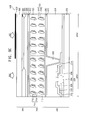
- FIG. 1 is a plan view illustrating a liquid crystal display panel according to an exemplary embodiment of the present invention.
- FIG. 2 is a cross-sectional view taken along a line I-I′ of FIG. 1 .
- FIGS. 3A , 3 B, 3 C, 3 D, 3 E, 3 F, and 3 G are cross-sectional views illustrating a method of manufacturing the liquid crystal display panel in FIGS. 1 and 2 .
- FIGS. 4A and 4B are graphs illustrating a transmittance of a liquid crystal layer according to a voltage between a pixel electrode and a common electrode.
- FIG. 5 is a cross-sectional view illustrating a liquid crystal display panel according to another exemplary embodiment of the present invention.
- FIGS. 6A , 6 B and 6 C are cross-sectional views illustrating a method of manufacturing the liquid crystal display panel in FIG. 5 .
- FIG. 7 is a graph illustrating a transmittance of a liquid crystal layer according to the voltage between the pixel electrode and the common electrode.
- FIGS. 8A and 8B are cross-sectional views illustrating a method of manufacturing the liquid crystal display panel according to still another exemplary embodiment of the present invention.
- FIG. 9 is a block diagram illustrating a liquid crystal display apparatus according to still another exemplary embodiment of the present invention.
- FIG. 1 is a plan view illustrating a liquid crystal display panel according to an exemplary embodiment of the present invention
- FIG. 2 is a cross-sectional view taken along a line I-I′ of FIG. 1 .
- the liquid crystal display panel 100 includes a lower substrate 200 , an upper substrate 300 and a liquid crystal layer 400 .
- the lower substrate 200 includes a first base substrate 202 , a thin-film transistor 220 , an organic insulating layer 250 and a pixel electrode 270 .
- the first base substrate 202 includes a first sub pixel area SPA1 and a second sub pixel area SPA2.
- the first sub pixel area SPA1 and the second sub pixel area SPA2 may form a pixel area.
- the first base substrate 202 may be a glass substrate or a plastic substrate.
- the thin-film transistor 220 is formed on the first base substrate 202 .
- the thin-film transistor 220 includes a gate electrode 204 extended from a gate line GL, a gate insulating layer 206 formed on the gate electrode 204 , an active layer 208 formed on the gate insulating layer 206 , an ohmic-contact layer 210 separately formed on the active layer 208 , a source electrode 212 formed on the ohmic-contact layer 210 and extended from a data line DL, and a drain electrode 214 formed on the ohmic-contact layer 210 and spaced apart from the source electrode 212 .
- the organic insulating layer 250 is formed on the thin-film transistor 220 to protect the thin-film transistor 220 . Although shown and described as a single organic insulating layer, layer 250 may include multiple layers. Furthermore, layer 250 may alternatively include an inorganic insulating layer and an organic insulating layer or multiple inorganic and organic insulating layers in any combination.
- the pixel electrode 270 is formed on the organic insulating layer 250 , and electrically connected to the drain electrode 214 of the thin-film transistor 220 through a contact hole 260 formed through the organic insulating layer 250 .
- the pixel electrode 270 may include a conductive material such as an indium tin oxide (ITO) or an indium zinc oxide (IZO).
- the upper substrate 300 includes a second base substrate 302 facing the first base substrate 202 , a color filter 304 formed on the second base substrate 302 , a light blocking layer 306 formed on the color filter 304 , an over-coating layer 308 formed on the color filter 304 and the light blocking layer 306 , and a common electrode 310 formed on the over-coating layer 308 .
- the liquid crystal layer 400 includes a first liquid crystal layer 410 and a second liquid crystal layer 420 .
- the first liquid crystal layer 410 is disposed in the first sub pixel area SPA1.
- the first liquid crystal layer 410 includes a first polymer 411 having a first pre-tilt.
- the first polymer 411 includes a first liquid crystal 412 and a first reactive mesogen 414 polymerized in the first liquid crystal 412 .
- the first reactive mesogen 414 may be an isotropic reactive mesogen.
- the first polymer 411 may be an isotropic polymer.
- the second liquid crystal layer 420 is disposed in the second sub pixel area SPA2.
- the second liquid crystal layer 420 includes a second polymer 421 having a second pre-tilt.
- the second pre-tilt may be less than the first pre-tilt.
- the second polymer 421 includes a second liquid crystal 422 and a second reactive mesogen 424 polymerized in the second liquid crystal 422 .
- the second reactive mesogen 424 may be an anisotropic reactive mesogen.
- the second polymer 421 may be an anisotropic polymer.
- the invention is not limited thereto, for example, the display apparatus may be configured such that the first polymer 411 is an anisotropic polymer and the second polymer 421 is an isotropic polymer.
- the liquid crystal display panel 100 may be a vertically aligned mode.
- the lower substrate 200 may further include a first alignment layer 280 formed on the pixel electrode 270 to align the first liquid crystal 412 and the second liquid crystal 422 .
- the upper substrate 300 may further include a second alignment layer 312 formed on the common electrode 310 to align the first liquid crystal 412 and the second liquid crystal 422 .
- FIGS. 3A to 3G are cross-sectional views illustrating a method of manufacturing the liquid crystal display panel 100 in FIGS. 1 and 2 .
- the lower substrate 200 is formed. Specifically, the thin-film transistor 220 is formed on the first base substrate 202 having the first sub pixel area SPA1 and the second sub pixel area SPA2, the organic insulating layer 250 is formed on the thin-film transistor 220 , and pixel electrode 270 is formed on the organic insulating layer 250 , and the first alignment layer 280 is formed on the pixel electrode 270 .
- the upper substrate 300 is formed. Specifically, the color filter 304 and the light blocking layer 306 are formed on the second base substrate 302 , the over-coating layer 308 is formed on the color filter 304 and the light blocking layer 306 , the common electrode 310 is formed on the over-coating layer 308 , and the second alignment layer 312 is formed on the common electrode 310 .
- the lower substrate 200 and the upper substrate 300 are combined, and a liquid crystal 402 and a reactive mesogen 404 are injected between the upper substrate and the lower substrate.
- the panel 101 is formed.
- the liquid crystal 402 may be an anisotropic liquid crystal
- the reactive mesogen 404 may be an anisotropic reactive mesogen.
- the liquid crystal 402 and the reactive mesogen 404 may be vertically aligned by the first alignment layer 280 and the second alignment layer 312 .
- heat is applied to the panel 101 to increase the temperature of the panel 101 .
- the temperature of the panel 101 may be increased to about 60° C.
- the reactive mesogen 404 may be converted to an isotropic reactive mesogen.
- the temperature of the panel 101 may be increased to about 90° C.
- the liquid crystal 402 may be converted to an isotropic liquid crystal, and the reactive mesogen 404 may be converted to an isotropic reactive mesogen.
- the temperature of the display panel may be increased or adjusted to other temperatures or ranges of temperatures.
- ultraviolet radiation UV is applied to the first sub pixel area SPA1 of the panel 101 .
- the liquid crystal 402 and the reactive mesogen 404 disposed in the first sub pixel area SPA1 are polymerized.
- a light blocking mask 500 may be disposed over the second sub pixel area SPA2 of the panel 101 .
- the liquid crystal 402 and the reactive mesogen 404 disposed in the second sub pixel area SPA2 are not polymerized.
- Heat may be applied to the panel 101 during the time period when UV radiation is also applied to the panel 101 as shown in FIG. 3E . Alternatively, heat may not be applied to the panel 101 during the time period when UV radiation is also applied to the panel 101
- the temperature of the panel 101 is decreased.
- the temperature of the panel 101 may be decreased to about 20° C.
- the first liquid crystal layer 410 including the first polymer 411 is formed in the first sub pixel area SPA1.
- the first polymer 411 may be the isotropic polymer including the isotropic reactive mesogen 414 .
- the liquid crystal 402 disposed in the second sub pixel area SPA2 is converted to an anisotropic liquid crystal
- the reactive mesogen 404 is converted to an anisotropic reactive mesogen.
- the temperature of the display panel can be increased adjusted to other temperatures or ranges of temperatures.
- the ultraviolet radiation UV is applied to the second sub pixel area SPA2 of the panel 101 . Therefore, the liquid crystal 402 and the reactive mesogen 404 disposed in the second sub pixel area SPA2 are polymerized, and thus the second liquid crystal 420 including the second polymer 421 in the second sub pixel area SPA2 is formed.
- the second polymer 421 may be the anisotropic polymer including an anisotropic reactive mesogen 424 .
- the liquid crystal layer 400 including the first liquid crystal layer 410 and the second liquid crystal layer 420 is formed, and the liquid crystal display panel 100 is formed.
- the ultraviolet radiation UV may be applied to both SPA1 and SPA2 simultaneously.
- the ultraviolet radiation UV may be applied only to the second sub pixel area SPA2 by using a light blocking mask such as the mask 500 in FIG. 3F to block the UV radiation incident on the first sub pixel area SPA1.
- FIGS. 4A and 4B are graphs illustrating a transmittance of the liquid crystal layer 400 according to the voltage between the pixel electrode 270 and the common electrode 310 .
- the content of the first reactive mesogen 414 and the second reactive mesogen 424 in the liquid crystal layer 400 may be about 1 wt %.
- the temperature of the panel 101 during which the ultraviolet ray UV is applied to the first sub pixel area SPA1 of the panel 101 may be about 60 degrees Celsius as illustrated in FIGS. 3D , 3 E and 4 A.
- the ultraviolet ray UV may be applied to the first sub pixel area SPA1 of the panel 101 for about 3 minutes, and the ultraviolet ray UV may be applied to the second sub pixel area SPA2 of the panel 101 for about 3 minutes.
- the dashed line graph shows a first voltage-transmittance characteristic indicating the dependence of the transmittance of the first liquid crystal layer 410 including the polymer 411 on the voltage between the pixel electrode 270 and the common electrode 310 .
- the solid line graph shows a second voltage-transmittance characteristic indicating the dependence of the transmittance of the second liquid crystal layer 420 including the polymer 421 on the voltage between the pixel electrode 270 and the common electrode 310 .
- the first voltage-transmittance characteristics corresponding to the first liquid crystal layer 410 disposed in the first pixel SPA1 is different from the second voltage characteristic corresponding to the second liquid crystal layer 420 disposed in the second pixel SPA2.
- a first thread voltage corresponding to the first liquid crystal layer 410 including the first polymer 411 is about 1.7 volts
- a second thread voltage corresponding to the second liquid crystal layer 420 including the second polymer 421 is about 2.3 volts.
- the first thread voltage corresponding to the first liquid crystal layer 410 is less than the second thread voltage corresponding to the second liquid crystal layer 420 .
- a first transmittance corresponding to the first liquid crystal layer 410 including the first polymer 411 is greater than a second transmittance corresponding to the second liquid crystal layer 420 including the second polymer 421 , when the first and the second transmittance are measured at the same voltage.
- the content of the first reactive mesogen 414 and the second reactive mesogen 424 in the liquid crystal layer 400 may be about 1 wt %.
- the temperature of the panel 101 during which the ultraviolet ray UV is applied to the first sub pixel area SPA1 of the panel 101 may be about 90° C. as illustrated in FIGS. 3D , 3 E and 4 B.
- the ultraviolet ray UV may be applied to the first sub pixel area SPA1 of the panel 101 for about 3 minutes, and the ultraviolet ray UV may be applied to the second sub pixel area SPA2 of the panel 101 for about 3 minutes.
- the dashed line graph shows a first voltage-transmittance characteristic indicating the dependence of the transmittance of the first liquid crystal layer 410 including the first polymer 411 on the voltage between the pixel electrode 270 and the common electrode 310 .
- the solid line graph shows a second voltage-transmittance characteristic indicating the dependence of the transmittance of the second liquid crystal layer 420 including the second polymer 421 on the voltage between the pixel electrode 270 and the common electrode 310 .
- the first voltage-transmittance characteristics corresponding to the first liquid crystal layer 410 disposed in the first pixel SPA1 is different from the second voltage-transmittance characteristic corresponding to the second liquid crystal layer 420 disposed in the second pixel SPA2.
- a first thread voltage corresponding to the first liquid crystal layer 410 including the first polymer 411 is about 1.9 volts
- a second thread voltage corresponding to the second liquid crystal layer 420 including the second polymer 421 is about 2.2 volts.
- the first thread voltage with respect to the first liquid crystal layer 410 is less than the second thread voltage with respect to the second liquid crystal layer 420 .
- a first transmittance corresponding to the first liquid crystal layer 410 including the first polymer 411 is greater than a second transmittance corresponding to the second liquid crystal layer 420 including the second polymer 421 , when the first and second transmittance are measured at the same voltage.
- the first pre-tilt of the first polymer 411 is greater than the second pre-tilt of the second polymer 421 , but the invention is not limited thereto.
- the first pre-tilt of the first polymer 411 may be less than the second pre-tilt of the second polymer 421 .
- the first liquid crystal layer 412 having a first pre-tilt and the second liquid crystal layer 422 having the second pre-tilt is manufactured by a method that does not involve the formation of an electric field between the pixel electrode 270 and the common electrode 310 before applying the ultraviolet ray UV to the panel 101 . Therefore a simple way of forming a pre-tilt is provided for both the first liquid crystal 412 and the second liquid crystal 422 of the liquid crystal layer 400 . Thus, the degradation of a contrast ratio that may occur during a process of forming the pre-tilt by applying an electric field may be prevented, and a response speed of the first liquid crystal 412 and the second liquid crystal 422 may be increased.
- the first liquid crystal 412 disposed in the first sub pixel area SPA1 has the first pre-tilt
- the second liquid crystal 422 disposed in the second sub pixel area SPA2 has the second pre-tilt different from the first pre-tilt. Therefore, a multi-domain may be implemented, and thus a visibility angle of the liquid crystal display panel 100 may be increased.
- FIG. 5 is a cross-sectional view illustrating a liquid crystal display panel according to another exemplary embodiment of the present invention.
- the liquid crystal display panel 600 according to this exemplary embodiment is substantially the same as the liquid crystal display panel 100 according to the previous exemplary embodiment illustrated in FIGS. 1 and 2 except for the liquid crystal layer 700 .
- the same reference numerals will be used to refer to same or like parts as those described in the previous exemplary embodiment and any further repetitive explanation concerning the above elements will be omitted.
- the liquid crystal display panel 600 includes the lower substrate 200 , the upper substrate 300 and the liquid crystal layer 700 .
- the liquid crystal layer 700 includes a first liquid crystal layer 710 and a second liquid crystal layer 720 .
- the first liquid crystal layer 710 is disposed in the first sub pixel area SPA1.
- the first liquid crystal layer 710 includes a first polymer 711 having a first pre-tilt.
- the first polymer 711 includes a first liquid crystal 712 and a first reactive mesogen 714 polymerized in the first liquid crystal 712 .
- the first reactive mesogen 714 may be an anisotropic reactive mesogen.
- the first polymer 711 may be an anisotropic polymer.
- the second liquid crystal layer 720 is disposed in the second sub pixel area SPA2.
- the second liquid crystal layer 720 includes a second polymer 721 having a second pre-tilt.
- the second pre-tilt may be less than the first pre-tilt.
- the second polymer 721 includes a second liquid crystal 722 and a second reactive mesogen 724 polymerized in the second liquid crystal 722 .
- the second reactive mesogen 724 may be an anisotropic reactive mesogen.
- the second polymer 721 may be an anisotropic polymer.
- the invention is not limited thereto, for example, the display apparatus may be configured such that the first polymer 711 is an anisotropic polymer and the second polymer 721 is an isotropic polymer.
- the liquid crystal display panel 600 may be vertically aligned mode.
- FIG. 6A to 6C are cross-sectional views illustrating a method of manufacturing the liquid crystal display panel 600 in FIG. 5 .
- a panel 601 is formed. Specifically, the lower substrate 200 is formed as illustrated in FIG. 3A .
- the upper substrate 300 is formed as illustrated in FIG. 3B .
- the lower substrate 200 and the upper substrate 300 are combined, and a liquid crystal 702 and a reactive mesogen 704 are injected between the lower substrate 200 and the upper substrate 300 .
- the panel 601 is formed.
- the liquid crystal 702 may be an anisotropic liquid crystal
- the reactive mesogen 704 may be an anisotropic reactive mesogen.
- the liquid crystal 702 and the reactive mesogen 704 may be vertically aligned by the first alignment layer 280 and the second alignment layer 312 .
- a light blocking mask 500 is disposed over the first sub pixel area SPA1 of the panel 601 , and a first ultraviolet ray UV1 is applied to the second sub pixel area SPA2 of the panel 601 . Therefore, the liquid crystal 702 and the reactive mesogen 704 disposed in the second sub pixel area SPA2 are polymerized, and thus the second liquid crystal layer 720 including the second polymer 721 is formed.
- the temperature of the display panel 601 may be kept essentially constant during the above described manufacturing processes. Alternatively, heat and cooling may be applied to the display panel 601 such that the temperature of the display panel may be increased and decreased in the same way as described with reference to FIGS. 3D , 3 E, 3 F and 3 G in the manufacturing of the liquid crystal display panel 100 shown in FIG. 3G . However the invention is not limited thereto. For example, heat and cooling may be applied to the display panel 601 according to manufacturing needs.
- the first ultraviolet ray UV1 has a first power density, and the first ultraviolet ray UV1 is applied to the second sub pixel area SPA2 for a first time period.
- the first power density of the first ultraviolet ray UV1 applied to the second sub pixel area SPA2 may be about 20 mW/cm 2
- the first ultraviolet ray UV1 may be applied to the second sub pixel area SPA2 for about 3 minutes.
- the light blocking mask 500 is disposed over the second sub pixel area SPA2 of the panel 601 , and a second ultraviolet ray UV2 is applied to the first sub pixel area SPA1 of the panel 601 . Therefore, the liquid crystal 702 and the reactive mesogen 704 disposed in the first sub pixel area SPA1 are polymerized, and thus the first liquid crystal layer 710 including the first polymer 711 is formed. Thus, the liquid crystal layer 700 including the first liquid crystal layer 710 and the second liquid crystal layer 720 is formed, and the liquid crystal display panel 600 is formed.
- the second ultraviolet ray UV2 has a second power density less than the first power density, and the second ultraviolet ray UV2 is applied to the first sub pixel area SPA1 of the panel 601 for a second time period longer than the first time period.
- the second power density of the second ultraviolet ray UV2 may be about 2 mW/cm 2
- the second ultraviolet ray UV2 may be applied to the first sub pixel area SPA1 for about 30 minutes.
- the first power density, the first time period, the second power density, and the second time period may be chosen such that the result of the multiplication between the first power density of the first ultraviolet ray UV1 and the first time period during which the first ultraviolet ray UV1 is applied to the second sub pixel area SPA2 may be equal to the result of the multiplication between the second power density of the second ultraviolet ray UV2 and the second time period during which the second ultraviolet ray UV2 is applied to the first sub pixel area SPA1.
- the energy applied to the second sub pixel SPA2 by the first ultraviolet ray UV1 may be substantially equal to the energy applied to the first sub pixel SPA1 by the second ultraviolet ray UV2.
- FIG. 7 is a graph illustrating a transmittance of the liquid crystal layer 700 according to the voltage between the pixel electrode 270 and the common electrode 310 .
- a content of the first reactive mesogen 714 and the second reactive mesogen 724 in the liquid crystal layer 400 may be about 1 wt %.
- a thread voltage for aligning the first polymer 711 and the second polymer 721 decreases with a decrease in power density of the ultraviolet ray and with an increase in the exposure time during which the ultraviolet ray is applied to the panel 601 .
- a first thread voltage with respect to the first polymer 711 is about 1.5 volts.
- a power density of the first ultraviolet ray UV1 applied to the second sub pixel area SPA2 is about 20 mW/cm 2 and the first ultraviolet ray UV1 is applied to the second sub pixel area SPA2 for about 3 minutes
- a second thread voltage with respect to the second polymer 721 is about 2.3 volts.
- the first thread voltage with respect to the first liquid crystal layer 710 is less than the second thread voltage with respect to the second liquid crystal layer 720 .
- the transmittance of the liquid crystal layer 700 is higher when the power density of the ultraviolet ray is lower and the time during which the ultraviolet ray is applied to the panel 601 is longer for the same voltage applied between the pixel electrode 270 and the common electrode 310 when the voltage is from about 1.9 volts to about 5.0 volts.
- a first transmittance corresponding to the first polymer 711 of the first liquid crystal layer 710 is greater than a second transmittance corresponding to the second polymer 721 of the second liquid crystal layer 720 .
- the first pre-tilt of the first polymer 711 is greater than the second pre-tilt of the second polymer 721 , but the invention is not limited thereto.
- the first pre-tilt of the first polymer 711 may be less than the second pre-tilt of the second polymer 721 .
- the first liquid crystal layer 712 having a first pre-tilt and the second liquid crystal layer 722 having the second pre-tilt is manufactured by a method that does not involve the formation of an electric field between the pixel electrode 270 and the common electrode 310 before applying the first ultraviolet ray UV1 and the second ultraviolet ray UV2 to the panel 601 . Therefore a simple way of forming a pre-tilt is provided for both the first liquid crystal 712 and the second liquid crystal 722 of the liquid crystal layer 700 . Thus, the degradation of a contrast ratio that may occur during a process of forming the pre-tilt by applying an electric field may be prevented, and a response speed of the first liquid crystal 712 and the second liquid crystal 722 may be increased.
- the first liquid crystal 712 disposed in the first sub pixel area SPA1 has the first pre-tilt
- the second liquid crystal 722 disposed in the second sub pixel area SPA2 has the second pre-tilt different from the first pre-tilt. Therefore, a multi-domain may be implemented, and thus a visibility angle of the liquid crystal display panel 600 may be increased.
- FIGS. 8A and 8B are cross-sectional views illustrating a method of manufacturing the liquid crystal display panel 600 according to still another exemplary embodiment of the present invention.
- the method of manufacturing the liquid crystal display panel 600 according to the present exemplary embodiment illustrated in FIGS. 8A and 8B may be the method of manufacturing the liquid crystal display panel 600 of the previous exemplary embodiment illustrated in FIG. 5 .
- the same reference numerals will be used to refer to same or like parts as those described in the previous exemplary embodiment and any further repetitive explanation concerning the above elements will be omitted.
- the panel 601 is formed. Specifically, the lower substrate 200 is formed as illustrated in FIG. 3A .
- the upper substrate 300 is formed as illustrated in FIG. 3B .
- the lower substrate 200 and the upper substrate 300 are combined, and the liquid crystal 702 and the reactive mesogen 704 are injected between the lower substrate 200 and the upper substrate 300 .
- the panel 601 is formed.
- the liquid crystal 702 may be an anisotropic liquid crystal
- the reactive mesogen 704 may be an anisotropic reactive mesogen.
- the liquid crystal 702 and the reactive mesogen 704 may be vertically aligned by the first alignment layer 280 and the second alignment layer 312 .
- a semi-transmittance mask 800 is disposed over the first sub pixel area SPA1 of the panel 601 , and an ultraviolet ray UV is applied to the first sub pixel area SPA1 and the second sub pixel area SPA2 of the panel 601 .
- the semi-transmittance mask 800 may absorb or block part of the ultraviolet radiation incident on the mask 800 and transmit part of the ultraviolet ray incident on the mask 800 to the sub pixel area SPA1.
- the transmittance of the mask 800 may be dependent on the wavelength of the incident ultraviolet radiation.
- the transmittance of the mask 800 may be adjusted according to panel manufacturing needs.
- the ultraviolet ray UV incident on the panel 601 has a first power density.
- the ultraviolet ray UV having the first power density is applied to the second sub pixel area SPA2, and the ultraviolet ray UV having a second power density less than the first power density is applied to the first sub pixel area SPA1.
- the ultraviolet ray UV may be applied to the first sub pixel area SPA1 and the second sub pixel area SPA2, and thus energy of the ultraviolet ray UV applied to the first sub pixel area SPA1 may be less than the energy of the ultraviolet ray UV applied to the second sub pixel area SPA2.
- the liquid crystal 702 and the reactive mesogen 704 disposed in the first sub pixel area SPA1 are polymerized, and thus the first liquid crystal layer 710 including the first polymer 711 having the first pre-tilt is formed.
- the liquid crystal 702 and the reactive mesogen 704 disposed in the second sub pixel area SPA2 are polymerized, and thus the second liquid crystal layer 720 including the second polymer 721 having the second pre-tilt is formed.
- the liquid crystal layer 700 including the first liquid crystal layer 710 and the second liquid crystal layer 720 is formed, and the liquid crystal display panel 600 is formed.
- the temperature of the display panel 601 may be kept essentially constant during the above described manufacturing processes.
- heat and cooling may be applied to the display panel 601 such that the temperature of the display panel may be increased and decreased in the same way as described with reference to FIGS. 3D , 3 E, 3 F and 3 G in the manufacturing of the liquid crystal display panel 100 shown in FIG. 3G .
- the invention is not limited thereto.
- heat and cooling may be applied to the display panel 601 according to manufacturing needs.
- the first liquid crystal layer 712 having a first pre-tilt and the second liquid crystal layer 722 having the second pre-tilt is manufactured by a method that does not involve the formation of an electric field between the pixel electrode 270 and the common electrode 310 before applying the ultraviolet ray to the panel 601 . Therefore a simple way of forming a pre-tilt is provided for both the first liquid crystal 712 and the second liquid crystal 722 of the liquid crystal layer 700 . Thus, the degradation of a contrast ratio that may occur during a process of forming the pre-tilt by applying an electric field may be prevented, and a response speed of the first liquid crystal 712 and the second liquid crystal 722 may be increased.
- the first liquid crystal 712 disposed in the first sub pixel area SPA1 has a first pre-tilt
- the second liquid crystal 722 disposed in the second sub pixel area SPA2 has a second pre-tilt different from the first pre-tilt. Therefore, a multi-domain may be implemented, and thus a visibility angle of the liquid crystal display panel 600 may be increased.
- FIG. 9 is a block diagram illustrating a liquid crystal display apparatus according to still another exemplary embodiment of the present invention.
- the liquid crystal display apparatus 900 includes a liquid crystal display panel 910 , a data driving part 920 , a gate driving part 930 and a timing control part 940 .
- the display panel 910 receives a data signal based on an image data DATA to display an image.
- the image data DATA may be a two-dimensional plane image data.
- the image data DATA may include a left-eye image data and a right-eye image data to display a three-dimensional stereoscopic image.
- the display panel 910 includes a plurality of gate lines GL substantially parallel with a first direction D1, a plurality of data lines DL substantially parallel with a second direction D2 substantially perpendicular to the first direction D1, and a plurality of pixels.
- the first direction D1 may be substantially parallel with a long side of the display panel 910
- the second direction D2 may be substantially parallel with a short side of the display panel 910 .
- the liquid crystal display panel 910 may be substantially the same as the liquid crystal display panel 100 according to the previous exemplary embodiment illustrated in FIGS. 1 and 2 .
- the liquid crystal display panel 910 may include the first sub pixel area SPA1 and the second sub pixel area SPA2.
- the first liquid crystal layer 410 including the first polymer 411 having the first pre-tilt may be disposed in the first sub pixel area SPA1
- the second liquid crystal layer 420 including the second polymer 421 having the second pre-tilt may be disposed in the second sub pixel area SPA2.
- the liquid crystal display panel 910 may be substantially the same as the liquid crystal display panel 600 according to the previous exemplary embodiment illustrated in FIG. 5 .
- the liquid crystal display panel 910 may include the first sub pixel area SPA1 and the second sub pixel area SPA2.
- the first liquid crystal layer 710 including the first polymer 711 having the first pre-tilt may be disposed in the first sub pixel area SPA1
- the second liquid crystal layer 720 including the second polymer 721 having the second pre-tilt may be disposed in the second sub pixel area SPA2.
- the liquid crystal display panel 910 may be manufactured by substantially the same method as the method of manufacturing a liquid crystal display panel according to the exemplary embodiments illustrated in FIGS. 8A and 8B .
- the data driving part 920 outputs data signals based on the image data DATA to the data lines DL in response to a first clock signal CLK1 and a horizontal start signal STH provided from the timing control part 940 .
- the gate driving part 930 generates gate signals using a vertical start signal STV and a second clock signal SLK2 provided from the timing control part 940 and outputs the gate signals to the gate lines GL.
- the timing control part 940 receives the image data DATA and a control signal CON from an outside.
- the control signal CON may include a horizontal synchronous signal Hsync, a vertical synchronous signal Vsync and a clock signal CLK.
- the timing control part 940 generates the horizontal start signal STH using the horizontal synchronous signal Hsync and outputs the horizontal start signal STH to the data driving part 920 .
- the timing control part 940 generates the vertical start signal STV using the vertical synchronous signal Vsync and outputs the vertical start signal STV to the gate driving part 930 .
- the timing control part 940 generates the first clock signal CLK1 and the second clock signal CLK2 using the clock signal CLK and outputs the first clock signal CLK1 to the data driving part 920 and the second clock signal CLK2 to the gate driving part 930 .
- the liquid crystal display panel 910 includes the first sub pixel area SPA1 and the second sub pixel area SPA2.
- the first liquid crystal layer 410 including the first polymer 411 having the first pre-tilt may be disposed in the first sub pixel area SPA1
- the second liquid crystal layer 420 including the second polymer 421 having the second pre-tilt may be disposed in the second sub pixel area SPA2.
- the first liquid crystal layer 710 including the first polymer 711 having the first pre-tilt may be disposed in the first sub pixel area SPA1
- the second liquid crystal layer 720 including the second polymer 721 having the second pre-tilt may be disposed in the second sub pixel area SPA2.
- the liquid crystal display panel 910 may be manufactured by substantially the same method as the method of manufacturing a liquid crystal display panel according to the exemplary embodiments illustrated in FIGS. 8A and 8B .
- a visibility angle of the liquid crystal display apparatus 100 may be increased, and a display quality of the liquid crystal display apparatus may be enhanced.
- a pre-tilt may be formed by a simple process for both the first liquid crystal disposed in a first sub pixel area and the second liquid crystal disposed in a second sub pixel area.
- degradation of a contrast ratio may be prevented, and a response speed of the first liquid crystal and the second liquid crystal may be increased.
- the first liquid crystal disposed in the first sub pixel area has a first pre-tilt
- the second liquid crystal disposed in the second sub pixel area has a second pre-tilt different from the first pre-tilt. Therefore, a multi-domain may be implemented, and thus a visibility angle of the liquid crystal display panel may be increased.
- a display quality of a liquid crystal display apparatus including the liquid crystal display panel may be enhanced.
Landscapes
- Physics & Mathematics (AREA)
- Nonlinear Science (AREA)
- Chemical & Material Sciences (AREA)
- Crystallography & Structural Chemistry (AREA)
- General Physics & Mathematics (AREA)
- Optics & Photonics (AREA)
- Mathematical Physics (AREA)
- Spectroscopy & Molecular Physics (AREA)
- Liquid Crystal (AREA)
- Dispersion Chemistry (AREA)
- Geometry (AREA)
Abstract
Description
Claims (7)
Applications Claiming Priority (2)
| Application Number | Priority Date | Filing Date | Title |
|---|---|---|---|
| KR1020120123960A KR102039966B1 (en) | 2012-11-05 | 2012-11-05 | Display panel, method of manufacturing the same and display apparatus having the same |
| KR10-2012-0123960 | 2012-11-05 |
Publications (2)
| Publication Number | Publication Date |
|---|---|
| US20140125895A1 US20140125895A1 (en) | 2014-05-08 |
| US9158159B2 true US9158159B2 (en) | 2015-10-13 |
Family
ID=50622034
Family Applications (1)
| Application Number | Title | Priority Date | Filing Date |
|---|---|---|---|
| US13/774,294 Expired - Fee Related US9158159B2 (en) | 2012-11-05 | 2013-02-22 | Liquid crystal display panel, method of manufacturing the same and liquid crystal display apparatus having the same |
Country Status (2)
| Country | Link |
|---|---|
| US (1) | US9158159B2 (en) |
| KR (1) | KR102039966B1 (en) |
Families Citing this family (3)
| Publication number | Priority date | Publication date | Assignee | Title |
|---|---|---|---|---|
| WO2016102015A1 (en) * | 2014-12-23 | 2016-06-30 | Consiglio Nazionale Delle Ricerche - Cnr | Multiple alignment method in liquid crystalline medium |
| CN107229157A (en) | 2016-03-25 | 2017-10-03 | 京东方科技集团股份有限公司 | Transparent display and preparation method thereof |
| CN111061096B (en) * | 2019-12-16 | 2022-07-12 | 深圳市华星光电半导体显示技术有限公司 | Display panel and manufacturing method thereof |
Citations (5)
| Publication number | Priority date | Publication date | Assignee | Title |
|---|---|---|---|---|
| JP2004302168A (en) | 2003-03-31 | 2004-10-28 | Fujitsu Display Technologies Corp | Manufacturing method of liquid crystal display device |
| US7102706B2 (en) | 2004-03-17 | 2006-09-05 | Boe Hydis Technology Co., Ltd. | Method for aligning polymer network liquid crystal |
| US20070070287A1 (en) * | 2005-09-29 | 2007-03-29 | Samsung Electronics Co., Ltd. | Liquid crystal display and manufacturing method thereof |
| US20100053526A1 (en) | 2008-08-27 | 2010-03-04 | Samsung Electronics Co., Ltd | Liquid crystal display panel and method of manufacturing the same |
| US20110212393A1 (en) * | 2008-02-26 | 2011-09-01 | Au Optronics Corporation | Methods for manufacturing pixel unit, liquid crystal display panel, and electro-optical apparatus |
Family Cites Families (3)
| Publication number | Priority date | Publication date | Assignee | Title |
|---|---|---|---|---|
| JP2004279904A (en) * | 2003-03-18 | 2004-10-07 | Fujitsu Display Technologies Corp | Liquid crystal display device and method of manufacturing the same |
| KR101615926B1 (en) * | 2009-07-28 | 2016-04-28 | 삼성디스플레이 주식회사 | Liquid crystal display device and method of manufacturing the same |
| JP5578132B2 (en) * | 2011-04-12 | 2014-08-27 | 凸版印刷株式会社 | Liquid crystal display |
-
2012
- 2012-11-05 KR KR1020120123960A patent/KR102039966B1/en not_active Expired - Fee Related
-
2013
- 2013-02-22 US US13/774,294 patent/US9158159B2/en not_active Expired - Fee Related
Patent Citations (5)
| Publication number | Priority date | Publication date | Assignee | Title |
|---|---|---|---|---|
| JP2004302168A (en) | 2003-03-31 | 2004-10-28 | Fujitsu Display Technologies Corp | Manufacturing method of liquid crystal display device |
| US7102706B2 (en) | 2004-03-17 | 2006-09-05 | Boe Hydis Technology Co., Ltd. | Method for aligning polymer network liquid crystal |
| US20070070287A1 (en) * | 2005-09-29 | 2007-03-29 | Samsung Electronics Co., Ltd. | Liquid crystal display and manufacturing method thereof |
| US20110212393A1 (en) * | 2008-02-26 | 2011-09-01 | Au Optronics Corporation | Methods for manufacturing pixel unit, liquid crystal display panel, and electro-optical apparatus |
| US20100053526A1 (en) | 2008-08-27 | 2010-03-04 | Samsung Electronics Co., Ltd | Liquid crystal display panel and method of manufacturing the same |
Also Published As
| Publication number | Publication date |
|---|---|
| KR20140057781A (en) | 2014-05-14 |
| KR102039966B1 (en) | 2019-11-05 |
| US20140125895A1 (en) | 2014-05-08 |
Similar Documents
| Publication | Publication Date | Title |
|---|---|---|
| CN102341743B (en) | Stereoscopic image display device | |
| KR20150071550A (en) | Liquid crystal display | |
| US20140211135A1 (en) | Liquid crystal display and method of manufacturing the same | |
| US9500925B2 (en) | Tri-state liquid crystal display panel | |
| TW201137473A (en) | Blue phase liquid crystal display and method for fabricating the same | |
| JP5450792B2 (en) | Liquid crystal display | |
| US9632369B2 (en) | Array substrate and manufacturing method thereof, as well as display device | |
| US9158159B2 (en) | Liquid crystal display panel, method of manufacturing the same and liquid crystal display apparatus having the same | |
| US9759959B2 (en) | Liquid crystal display | |
| US20160154282A1 (en) | Liquid crystal display | |
| WO2013100088A1 (en) | Liquid crystal display device | |
| JP5355775B2 (en) | Liquid crystal display | |
| CN104460067B (en) | Pixel includes the display panel and its broken wire repair method of the pixel | |
| KR102160112B1 (en) | Liquid crystal display | |
| WO2016067948A1 (en) | Liquid crystal display apparatus | |
| US9897859B2 (en) | Liquid crystal display panel and fabrication method | |
| WO2015174349A1 (en) | Liquid crystal display device | |
| CN105404057B (en) | Liquid crystal display panel | |
| US9459496B2 (en) | Display panel and display device | |
| US8848117B2 (en) | Display apparatus | |
| JP6262859B2 (en) | Liquid crystal display device and manufacturing method thereof | |
| TW202040235A (en) | Display apparatus | |
| US9804447B2 (en) | Liquid crystal display and manufacturing method thereof | |
| US9500914B2 (en) | Liquid crystal display apparatus and manufacturing method thereof | |
| CN202995199U (en) | Blue-phase LCD (liquid crystal display) |
Legal Events
| Date | Code | Title | Description |
|---|---|---|---|
| AS | Assignment |
Owner name: PUSAN NATIONAL UNIVERSITY INDUSTRY-UNIVERSITY COOP Free format text: ASSIGNMENT OF ASSIGNORS INTEREST;ASSIGNORS:KIM, HOON;SHIN, KI-CHUL;YOON, TAE-HOON;AND OTHERS;SIGNING DATES FROM 20130115 TO 20130210;REEL/FRAME:029860/0166 Owner name: SAMSUNG DISPLAY CO., LTD., KOREA, REPUBLIC OF Free format text: ASSIGNMENT OF ASSIGNORS INTEREST;ASSIGNORS:KIM, HOON;SHIN, KI-CHUL;YOON, TAE-HOON;AND OTHERS;SIGNING DATES FROM 20130115 TO 20130210;REEL/FRAME:029860/0166 |
|
| FEPP | Fee payment procedure |
Free format text: PAYOR NUMBER ASSIGNED (ORIGINAL EVENT CODE: ASPN); ENTITY STATUS OF PATENT OWNER: LARGE ENTITY |
|
| STCF | Information on status: patent grant |
Free format text: PATENTED CASE |
|
| MAFP | Maintenance fee payment |
Free format text: PAYMENT OF MAINTENANCE FEE, 4TH YEAR, LARGE ENTITY (ORIGINAL EVENT CODE: M1551); ENTITY STATUS OF PATENT OWNER: LARGE ENTITY Year of fee payment: 4 |
|
| FEPP | Fee payment procedure |
Free format text: MAINTENANCE FEE REMINDER MAILED (ORIGINAL EVENT CODE: REM.); ENTITY STATUS OF PATENT OWNER: LARGE ENTITY |
|
| LAPS | Lapse for failure to pay maintenance fees |
Free format text: PATENT EXPIRED FOR FAILURE TO PAY MAINTENANCE FEES (ORIGINAL EVENT CODE: EXP.); ENTITY STATUS OF PATENT OWNER: LARGE ENTITY |
|
| STCH | Information on status: patent discontinuation |
Free format text: PATENT EXPIRED DUE TO NONPAYMENT OF MAINTENANCE FEES UNDER 37 CFR 1.362 |
|
| FP | Lapsed due to failure to pay maintenance fee |
Effective date: 20231013 |