US9123663B2 - Semiconductor device and method of forming shielding layer grounded through metal pillars formed in peripheral region of the semiconductor - Google Patents
Semiconductor device and method of forming shielding layer grounded through metal pillars formed in peripheral region of the semiconductor Download PDFInfo
- Publication number
- US9123663B2 US9123663B2 US12/136,682 US13668208A US9123663B2 US 9123663 B2 US9123663 B2 US 9123663B2 US 13668208 A US13668208 A US 13668208A US 9123663 B2 US9123663 B2 US 9123663B2
- Authority
- US
- United States
- Prior art keywords
- substrate
- semiconductor die
- shielding layer
- forming
- semiconductor
- Prior art date
- Legal status (The legal status is an assumption and is not a legal conclusion. Google has not performed a legal analysis and makes no representation as to the accuracy of the status listed.)
- Active, expires
Links
- 239000004065 semiconductor Substances 0.000 title claims abstract description 164
- 229910052751 metal Inorganic materials 0.000 title claims abstract description 46
- 239000002184 metal Substances 0.000 title claims abstract description 46
- 238000000034 method Methods 0.000 title claims description 35
- 230000002093 peripheral effect Effects 0.000 title claims description 13
- 239000000758 substrate Substances 0.000 claims abstract description 120
- 239000008393 encapsulating agent Substances 0.000 claims abstract description 38
- 229910000679 solder Inorganic materials 0.000 claims description 36
- 239000000463 material Substances 0.000 claims description 32
- 238000004519 manufacturing process Methods 0.000 claims description 18
- 239000010949 copper Substances 0.000 claims description 10
- 229910052802 copper Inorganic materials 0.000 claims description 9
- 229910052782 aluminium Inorganic materials 0.000 claims description 7
- 238000000465 moulding Methods 0.000 claims description 5
- 150000001875 compounds Chemical class 0.000 claims description 4
- RYGMFSIKBFXOCR-UHFFFAOYSA-N Copper Chemical group [Cu] RYGMFSIKBFXOCR-UHFFFAOYSA-N 0.000 claims description 3
- 229910001209 Low-carbon steel Inorganic materials 0.000 claims description 3
- 229910000831 Steel Inorganic materials 0.000 claims description 3
- XAGFODPZIPBFFR-UHFFFAOYSA-N aluminium Chemical compound [Al] XAGFODPZIPBFFR-UHFFFAOYSA-N 0.000 claims description 3
- 238000005553 drilling Methods 0.000 claims description 3
- XWHPIFXRKKHEKR-UHFFFAOYSA-N iron silicon Chemical compound [Si].[Fe] XWHPIFXRKKHEKR-UHFFFAOYSA-N 0.000 claims description 3
- MOFOBJHOKRNACT-UHFFFAOYSA-N nickel silver Chemical compound [Ni].[Ag] MOFOBJHOKRNACT-UHFFFAOYSA-N 0.000 claims description 3
- 239000010956 nickel silver Substances 0.000 claims description 3
- 229910001220 stainless steel Inorganic materials 0.000 claims description 3
- 239000010935 stainless steel Substances 0.000 claims description 3
- 239000010959 steel Substances 0.000 claims description 3
- 238000000151 deposition Methods 0.000 claims 3
- ZGHQUYZPMWMLBM-UHFFFAOYSA-N 1,2-dichloro-4-phenylbenzene Chemical compound C1=C(Cl)C(Cl)=CC=C1C1=CC=CC=C1 ZGHQUYZPMWMLBM-UHFFFAOYSA-N 0.000 description 19
- 230000008569 process Effects 0.000 description 16
- 239000004020 conductor Substances 0.000 description 10
- 239000011135 tin Substances 0.000 description 10
- ZLGYJAIAVPVCNF-UHFFFAOYSA-N 1,2,4-trichloro-5-(3,5-dichlorophenyl)benzene Chemical compound ClC1=CC(Cl)=CC(C=2C(=CC(Cl)=C(Cl)C=2)Cl)=C1 ZLGYJAIAVPVCNF-UHFFFAOYSA-N 0.000 description 9
- 239000011133 lead Substances 0.000 description 9
- PXHVJJICTQNCMI-UHFFFAOYSA-N Nickel Chemical compound [Ni] PXHVJJICTQNCMI-UHFFFAOYSA-N 0.000 description 8
- 238000005520 cutting process Methods 0.000 description 8
- 230000006870 function Effects 0.000 description 8
- 239000010931 gold Substances 0.000 description 8
- 230000008878 coupling Effects 0.000 description 7
- 238000010168 coupling process Methods 0.000 description 7
- 238000005859 coupling reaction Methods 0.000 description 7
- 238000007772 electroless plating Methods 0.000 description 7
- 238000009713 electroplating Methods 0.000 description 7
- 229910052737 gold Inorganic materials 0.000 description 7
- RUEIBQJFGMERJD-UHFFFAOYSA-N 1,2,3,4,5-pentachloro-6-(2-chlorophenyl)benzene Chemical compound ClC1=CC=CC=C1C1=C(Cl)C(Cl)=C(Cl)C(Cl)=C1Cl RUEIBQJFGMERJD-UHFFFAOYSA-N 0.000 description 6
- HOPMUCXYRNOABF-UHFFFAOYSA-N 1,2,3,4-tetrachloro-5-(2,3,5-trichlorophenyl)benzene Chemical compound ClC1=CC(Cl)=C(Cl)C(C=2C(=C(Cl)C(Cl)=C(Cl)C=2)Cl)=C1 HOPMUCXYRNOABF-UHFFFAOYSA-N 0.000 description 6
- 239000003990 capacitor Substances 0.000 description 6
- 238000005229 chemical vapour deposition Methods 0.000 description 6
- 229910052759 nickel Inorganic materials 0.000 description 6
- 239000010944 silver (metal) Substances 0.000 description 6
- 229910052718 tin Inorganic materials 0.000 description 6
- 238000013461 design Methods 0.000 description 5
- 238000005240 physical vapour deposition Methods 0.000 description 5
- 230000015572 biosynthetic process Effects 0.000 description 4
- 238000004891 communication Methods 0.000 description 4
- -1 e.g. Substances 0.000 description 4
- 239000004593 Epoxy Substances 0.000 description 3
- 239000000853 adhesive Substances 0.000 description 3
- 230000001070 adhesive effect Effects 0.000 description 3
- 230000007613 environmental effect Effects 0.000 description 3
- 230000005496 eutectics Effects 0.000 description 3
- 230000008020 evaporation Effects 0.000 description 3
- 238000001704 evaporation Methods 0.000 description 3
- 230000001939 inductive effect Effects 0.000 description 3
- 239000011810 insulating material Substances 0.000 description 3
- 238000002955 isolation Methods 0.000 description 3
- 238000004806 packaging method and process Methods 0.000 description 3
- 229910052709 silver Inorganic materials 0.000 description 3
- 229910045601 alloy Inorganic materials 0.000 description 2
- 239000000956 alloy Substances 0.000 description 2
- 239000000919 ceramic Substances 0.000 description 2
- 239000002131 composite material Substances 0.000 description 2
- 239000011521 glass Substances 0.000 description 2
- 238000010438 heat treatment Methods 0.000 description 2
- 238000001465 metallisation Methods 0.000 description 2
- 150000002739 metals Chemical class 0.000 description 2
- 238000012986 modification Methods 0.000 description 2
- 230000004048 modification Effects 0.000 description 2
- 239000004033 plastic Substances 0.000 description 2
- 229920003023 plastic Polymers 0.000 description 2
- 229920000642 polymer Polymers 0.000 description 2
- 238000012545 processing Methods 0.000 description 2
- 238000007650 screen-printing Methods 0.000 description 2
- 229910052710 silicon Inorganic materials 0.000 description 2
- 239000010703 silicon Substances 0.000 description 2
- FRWYFWZENXDZMU-UHFFFAOYSA-N 2-iodoquinoline Chemical compound C1=CC=CC2=NC(I)=CC=C21 FRWYFWZENXDZMU-UHFFFAOYSA-N 0.000 description 1
- BQCADISMDOOEFD-UHFFFAOYSA-N Silver Chemical compound [Ag] BQCADISMDOOEFD-UHFFFAOYSA-N 0.000 description 1
- ATJFFYVFTNAWJD-UHFFFAOYSA-N Tin Chemical compound [Sn] ATJFFYVFTNAWJD-UHFFFAOYSA-N 0.000 description 1
- OFLYIWITHZJFLS-UHFFFAOYSA-N [Si].[Au] Chemical compound [Si].[Au] OFLYIWITHZJFLS-UHFFFAOYSA-N 0.000 description 1
- 230000006978 adaptation Effects 0.000 description 1
- 230000002411 adverse Effects 0.000 description 1
- LTPBRCUWZOMYOC-UHFFFAOYSA-N beryllium oxide Inorganic materials O=[Be] LTPBRCUWZOMYOC-UHFFFAOYSA-N 0.000 description 1
- 229910052797 bismuth Inorganic materials 0.000 description 1
- 230000000903 blocking effect Effects 0.000 description 1
- 239000000356 contaminant Substances 0.000 description 1
- 239000013078 crystal Substances 0.000 description 1
- 238000009792 diffusion process Methods 0.000 description 1
- 239000002019 doping agent Substances 0.000 description 1
- 230000009977 dual effect Effects 0.000 description 1
- 230000005684 electric field Effects 0.000 description 1
- 238000010292 electrical insulation Methods 0.000 description 1
- 239000003822 epoxy resin Substances 0.000 description 1
- 238000005530 etching Methods 0.000 description 1
- 230000004907 flux Effects 0.000 description 1
- PCHJSUWPFVWCPO-UHFFFAOYSA-N gold Chemical compound [Au] PCHJSUWPFVWCPO-UHFFFAOYSA-N 0.000 description 1
- 230000006698 induction Effects 0.000 description 1
- 238000005468 ion implantation Methods 0.000 description 1
- 229910052745 lead Inorganic materials 0.000 description 1
- 239000007788 liquid Substances 0.000 description 1
- 230000000873 masking effect Effects 0.000 description 1
- 230000008018 melting Effects 0.000 description 1
- 238000002844 melting Methods 0.000 description 1
- 230000015654 memory Effects 0.000 description 1
- 238000002156 mixing Methods 0.000 description 1
- 230000003647 oxidation Effects 0.000 description 1
- 238000007254 oxidation reaction Methods 0.000 description 1
- 239000005022 packaging material Substances 0.000 description 1
- 239000002245 particle Substances 0.000 description 1
- 238000000059 patterning Methods 0.000 description 1
- 230000000737 periodic effect Effects 0.000 description 1
- 238000000206 photolithography Methods 0.000 description 1
- 238000007747 plating Methods 0.000 description 1
- 229920000647 polyepoxide Polymers 0.000 description 1
- 239000002861 polymer material Substances 0.000 description 1
- KCTAWXVAICEBSD-UHFFFAOYSA-N prop-2-enoyloxy prop-2-eneperoxoate Chemical compound C=CC(=O)OOOC(=O)C=C KCTAWXVAICEBSD-UHFFFAOYSA-N 0.000 description 1
- 230000035945 sensitivity Effects 0.000 description 1
- HBMJWWWQQXIZIP-UHFFFAOYSA-N silicon carbide Chemical compound [Si+]#[C-] HBMJWWWQQXIZIP-UHFFFAOYSA-N 0.000 description 1
- 229910010271 silicon carbide Inorganic materials 0.000 description 1
- 239000004332 silver Substances 0.000 description 1
- 238000004544 sputter deposition Methods 0.000 description 1
- 230000001360 synchronised effect Effects 0.000 description 1
- JBQYATWDVHIOAR-UHFFFAOYSA-N tellanylidenegermanium Chemical compound [Te]=[Ge] JBQYATWDVHIOAR-UHFFFAOYSA-N 0.000 description 1
- 238000001721 transfer moulding Methods 0.000 description 1
Images


Classifications
-
- H—ELECTRICITY
- H01—ELECTRIC ELEMENTS
- H01L—SEMICONDUCTOR DEVICES NOT COVERED BY CLASS H10
- H01L23/00—Details of semiconductor or other solid state devices
- H01L23/28—Encapsulations, e.g. encapsulating layers, coatings, e.g. for protection
- H01L23/31—Encapsulations, e.g. encapsulating layers, coatings, e.g. for protection characterised by the arrangement or shape
- H01L23/3107—Encapsulations, e.g. encapsulating layers, coatings, e.g. for protection characterised by the arrangement or shape the device being completely enclosed
- H01L23/3121—Encapsulations, e.g. encapsulating layers, coatings, e.g. for protection characterised by the arrangement or shape the device being completely enclosed a substrate forming part of the encapsulation
-
- H—ELECTRICITY
- H01—ELECTRIC ELEMENTS
- H01L—SEMICONDUCTOR DEVICES NOT COVERED BY CLASS H10
- H01L21/00—Processes or apparatus adapted for the manufacture or treatment of semiconductor or solid state devices or of parts thereof
- H01L21/02—Manufacture or treatment of semiconductor devices or of parts thereof
- H01L21/04—Manufacture or treatment of semiconductor devices or of parts thereof the devices having at least one potential-jump barrier or surface barrier, e.g. PN junction, depletion layer or carrier concentration layer
- H01L21/50—Assembly of semiconductor devices using processes or apparatus not provided for in a single one of the subgroups H01L21/06 - H01L21/326, e.g. sealing of a cap to a base of a container
- H01L21/56—Encapsulations, e.g. encapsulation layers, coatings
- H01L21/561—Batch processing
-
- H—ELECTRICITY
- H01—ELECTRIC ELEMENTS
- H01L—SEMICONDUCTOR DEVICES NOT COVERED BY CLASS H10
- H01L23/00—Details of semiconductor or other solid state devices
- H01L23/28—Encapsulations, e.g. encapsulating layers, coatings, e.g. for protection
- H01L23/29—Encapsulations, e.g. encapsulating layers, coatings, e.g. for protection characterised by the material, e.g. carbon
-
- H—ELECTRICITY
- H01—ELECTRIC ELEMENTS
- H01L—SEMICONDUCTOR DEVICES NOT COVERED BY CLASS H10
- H01L23/00—Details of semiconductor or other solid state devices
- H01L23/28—Encapsulations, e.g. encapsulating layers, coatings, e.g. for protection
- H01L23/31—Encapsulations, e.g. encapsulating layers, coatings, e.g. for protection characterised by the arrangement or shape
- H01L23/3107—Encapsulations, e.g. encapsulating layers, coatings, e.g. for protection characterised by the arrangement or shape the device being completely enclosed
- H01L23/3121—Encapsulations, e.g. encapsulating layers, coatings, e.g. for protection characterised by the arrangement or shape the device being completely enclosed a substrate forming part of the encapsulation
- H01L23/3128—Encapsulations, e.g. encapsulating layers, coatings, e.g. for protection characterised by the arrangement or shape the device being completely enclosed a substrate forming part of the encapsulation the substrate having spherical bumps for external connection
-
- H—ELECTRICITY
- H01—ELECTRIC ELEMENTS
- H01L—SEMICONDUCTOR DEVICES NOT COVERED BY CLASS H10
- H01L23/00—Details of semiconductor or other solid state devices
- H01L23/552—Protection against radiation, e.g. light or electromagnetic waves
-
- H—ELECTRICITY
- H01—ELECTRIC ELEMENTS
- H01L—SEMICONDUCTOR DEVICES NOT COVERED BY CLASS H10
- H01L24/00—Arrangements for connecting or disconnecting semiconductor or solid-state bodies; Methods or apparatus related thereto
- H01L24/93—Batch processes
- H01L24/95—Batch processes at chip-level, i.e. with connecting carried out on a plurality of singulated devices, i.e. on diced chips
- H01L24/97—Batch processes at chip-level, i.e. with connecting carried out on a plurality of singulated devices, i.e. on diced chips the devices being connected to a common substrate, e.g. interposer, said common substrate being separable into individual assemblies after connecting
-
- H—ELECTRICITY
- H01—ELECTRIC ELEMENTS
- H01L—SEMICONDUCTOR DEVICES NOT COVERED BY CLASS H10
- H01L2224/00—Indexing scheme for arrangements for connecting or disconnecting semiconductor or solid-state bodies and methods related thereto as covered by H01L24/00
- H01L2224/01—Means for bonding being attached to, or being formed on, the surface to be connected, e.g. chip-to-package, die-attach, "first-level" interconnects; Manufacturing methods related thereto
- H01L2224/02—Bonding areas; Manufacturing methods related thereto
- H01L2224/04—Structure, shape, material or disposition of the bonding areas prior to the connecting process
- H01L2224/05—Structure, shape, material or disposition of the bonding areas prior to the connecting process of an individual bonding area
- H01L2224/0554—External layer
- H01L2224/0556—Disposition
- H01L2224/05568—Disposition the whole external layer protruding from the surface
-
- H—ELECTRICITY
- H01—ELECTRIC ELEMENTS
- H01L—SEMICONDUCTOR DEVICES NOT COVERED BY CLASS H10
- H01L2224/00—Indexing scheme for arrangements for connecting or disconnecting semiconductor or solid-state bodies and methods related thereto as covered by H01L24/00
- H01L2224/01—Means for bonding being attached to, or being formed on, the surface to be connected, e.g. chip-to-package, die-attach, "first-level" interconnects; Manufacturing methods related thereto
- H01L2224/02—Bonding areas; Manufacturing methods related thereto
- H01L2224/04—Structure, shape, material or disposition of the bonding areas prior to the connecting process
- H01L2224/05—Structure, shape, material or disposition of the bonding areas prior to the connecting process of an individual bonding area
- H01L2224/0554—External layer
- H01L2224/05573—Single external layer
-
- H—ELECTRICITY
- H01—ELECTRIC ELEMENTS
- H01L—SEMICONDUCTOR DEVICES NOT COVERED BY CLASS H10
- H01L2224/00—Indexing scheme for arrangements for connecting or disconnecting semiconductor or solid-state bodies and methods related thereto as covered by H01L24/00
- H01L2224/01—Means for bonding being attached to, or being formed on, the surface to be connected, e.g. chip-to-package, die-attach, "first-level" interconnects; Manufacturing methods related thereto
- H01L2224/10—Bump connectors; Manufacturing methods related thereto
- H01L2224/15—Structure, shape, material or disposition of the bump connectors after the connecting process
- H01L2224/16—Structure, shape, material or disposition of the bump connectors after the connecting process of an individual bump connector
- H01L2224/161—Disposition
- H01L2224/16151—Disposition the bump connector connecting between a semiconductor or solid-state body and an item not being a semiconductor or solid-state body, e.g. chip-to-substrate, chip-to-passive
- H01L2224/16221—Disposition the bump connector connecting between a semiconductor or solid-state body and an item not being a semiconductor or solid-state body, e.g. chip-to-substrate, chip-to-passive the body and the item being stacked
- H01L2224/16225—Disposition the bump connector connecting between a semiconductor or solid-state body and an item not being a semiconductor or solid-state body, e.g. chip-to-substrate, chip-to-passive the body and the item being stacked the item being non-metallic, e.g. insulating substrate with or without metallisation
-
- H—ELECTRICITY
- H01—ELECTRIC ELEMENTS
- H01L—SEMICONDUCTOR DEVICES NOT COVERED BY CLASS H10
- H01L2224/00—Indexing scheme for arrangements for connecting or disconnecting semiconductor or solid-state bodies and methods related thereto as covered by H01L24/00
- H01L2224/01—Means for bonding being attached to, or being formed on, the surface to be connected, e.g. chip-to-package, die-attach, "first-level" interconnects; Manufacturing methods related thereto
- H01L2224/42—Wire connectors; Manufacturing methods related thereto
- H01L2224/47—Structure, shape, material or disposition of the wire connectors after the connecting process
- H01L2224/48—Structure, shape, material or disposition of the wire connectors after the connecting process of an individual wire connector
- H01L2224/4805—Shape
- H01L2224/4809—Loop shape
- H01L2224/48091—Arched
-
- H—ELECTRICITY
- H01—ELECTRIC ELEMENTS
- H01L—SEMICONDUCTOR DEVICES NOT COVERED BY CLASS H10
- H01L2224/00—Indexing scheme for arrangements for connecting or disconnecting semiconductor or solid-state bodies and methods related thereto as covered by H01L24/00
- H01L2224/73—Means for bonding being of different types provided for in two or more of groups H01L2224/10, H01L2224/18, H01L2224/26, H01L2224/34, H01L2224/42, H01L2224/50, H01L2224/63, H01L2224/71
- H01L2224/732—Location after the connecting process
- H01L2224/73251—Location after the connecting process on different surfaces
- H01L2224/73265—Layer and wire connectors
-
- H—ELECTRICITY
- H01—ELECTRIC ELEMENTS
- H01L—SEMICONDUCTOR DEVICES NOT COVERED BY CLASS H10
- H01L2224/00—Indexing scheme for arrangements for connecting or disconnecting semiconductor or solid-state bodies and methods related thereto as covered by H01L24/00
- H01L2224/80—Methods for connecting semiconductor or other solid state bodies using means for bonding being attached to, or being formed on, the surface to be connected
- H01L2224/81—Methods for connecting semiconductor or other solid state bodies using means for bonding being attached to, or being formed on, the surface to be connected using a bump connector
-
- H—ELECTRICITY
- H01—ELECTRIC ELEMENTS
- H01L—SEMICONDUCTOR DEVICES NOT COVERED BY CLASS H10
- H01L2224/00—Indexing scheme for arrangements for connecting or disconnecting semiconductor or solid-state bodies and methods related thereto as covered by H01L24/00
- H01L2224/93—Batch processes
- H01L2224/95—Batch processes at chip-level, i.e. with connecting carried out on a plurality of singulated devices, i.e. on diced chips
- H01L2224/97—Batch processes at chip-level, i.e. with connecting carried out on a plurality of singulated devices, i.e. on diced chips the devices being connected to a common substrate, e.g. interposer, said common substrate being separable into individual assemblies after connecting
-
- H—ELECTRICITY
- H01—ELECTRIC ELEMENTS
- H01L—SEMICONDUCTOR DEVICES NOT COVERED BY CLASS H10
- H01L24/00—Arrangements for connecting or disconnecting semiconductor or solid-state bodies; Methods or apparatus related thereto
- H01L24/01—Means for bonding being attached to, or being formed on, the surface to be connected, e.g. chip-to-package, die-attach, "first-level" interconnects; Manufacturing methods related thereto
- H01L24/42—Wire connectors; Manufacturing methods related thereto
- H01L24/47—Structure, shape, material or disposition of the wire connectors after the connecting process
- H01L24/48—Structure, shape, material or disposition of the wire connectors after the connecting process of an individual wire connector
-
- H—ELECTRICITY
- H01—ELECTRIC ELEMENTS
- H01L—SEMICONDUCTOR DEVICES NOT COVERED BY CLASS H10
- H01L2924/00—Indexing scheme for arrangements or methods for connecting or disconnecting semiconductor or solid-state bodies as covered by H01L24/00
- H01L2924/0001—Technical content checked by a classifier
- H01L2924/00014—Technical content checked by a classifier the subject-matter covered by the group, the symbol of which is combined with the symbol of this group, being disclosed without further technical details
-
- H—ELECTRICITY
- H01—ELECTRIC ELEMENTS
- H01L—SEMICONDUCTOR DEVICES NOT COVERED BY CLASS H10
- H01L2924/00—Indexing scheme for arrangements or methods for connecting or disconnecting semiconductor or solid-state bodies as covered by H01L24/00
- H01L2924/01—Chemical elements
- H01L2924/01004—Beryllium [Be]
-
- H—ELECTRICITY
- H01—ELECTRIC ELEMENTS
- H01L—SEMICONDUCTOR DEVICES NOT COVERED BY CLASS H10
- H01L2924/00—Indexing scheme for arrangements or methods for connecting or disconnecting semiconductor or solid-state bodies as covered by H01L24/00
- H01L2924/01—Chemical elements
- H01L2924/01006—Carbon [C]
-
- H—ELECTRICITY
- H01—ELECTRIC ELEMENTS
- H01L—SEMICONDUCTOR DEVICES NOT COVERED BY CLASS H10
- H01L2924/00—Indexing scheme for arrangements or methods for connecting or disconnecting semiconductor or solid-state bodies as covered by H01L24/00
- H01L2924/01—Chemical elements
- H01L2924/01013—Aluminum [Al]
-
- H—ELECTRICITY
- H01—ELECTRIC ELEMENTS
- H01L—SEMICONDUCTOR DEVICES NOT COVERED BY CLASS H10
- H01L2924/00—Indexing scheme for arrangements or methods for connecting or disconnecting semiconductor or solid-state bodies as covered by H01L24/00
- H01L2924/01—Chemical elements
- H01L2924/01029—Copper [Cu]
-
- H—ELECTRICITY
- H01—ELECTRIC ELEMENTS
- H01L—SEMICONDUCTOR DEVICES NOT COVERED BY CLASS H10
- H01L2924/00—Indexing scheme for arrangements or methods for connecting or disconnecting semiconductor or solid-state bodies as covered by H01L24/00
- H01L2924/01—Chemical elements
- H01L2924/0103—Zinc [Zn]
-
- H—ELECTRICITY
- H01—ELECTRIC ELEMENTS
- H01L—SEMICONDUCTOR DEVICES NOT COVERED BY CLASS H10
- H01L2924/00—Indexing scheme for arrangements or methods for connecting or disconnecting semiconductor or solid-state bodies as covered by H01L24/00
- H01L2924/01—Chemical elements
- H01L2924/01047—Silver [Ag]
-
- H—ELECTRICITY
- H01—ELECTRIC ELEMENTS
- H01L—SEMICONDUCTOR DEVICES NOT COVERED BY CLASS H10
- H01L2924/00—Indexing scheme for arrangements or methods for connecting or disconnecting semiconductor or solid-state bodies as covered by H01L24/00
- H01L2924/01—Chemical elements
- H01L2924/01078—Platinum [Pt]
-
- H—ELECTRICITY
- H01—ELECTRIC ELEMENTS
- H01L—SEMICONDUCTOR DEVICES NOT COVERED BY CLASS H10
- H01L2924/00—Indexing scheme for arrangements or methods for connecting or disconnecting semiconductor or solid-state bodies as covered by H01L24/00
- H01L2924/01—Chemical elements
- H01L2924/01079—Gold [Au]
-
- H—ELECTRICITY
- H01—ELECTRIC ELEMENTS
- H01L—SEMICONDUCTOR DEVICES NOT COVERED BY CLASS H10
- H01L2924/00—Indexing scheme for arrangements or methods for connecting or disconnecting semiconductor or solid-state bodies as covered by H01L24/00
- H01L2924/01—Chemical elements
- H01L2924/01082—Lead [Pb]
-
- H—ELECTRICITY
- H01—ELECTRIC ELEMENTS
- H01L—SEMICONDUCTOR DEVICES NOT COVERED BY CLASS H10
- H01L2924/00—Indexing scheme for arrangements or methods for connecting or disconnecting semiconductor or solid-state bodies as covered by H01L24/00
- H01L2924/013—Alloys
- H01L2924/0132—Binary Alloys
- H01L2924/01322—Eutectic Alloys, i.e. obtained by a liquid transforming into two solid phases
-
- H—ELECTRICITY
- H01—ELECTRIC ELEMENTS
- H01L—SEMICONDUCTOR DEVICES NOT COVERED BY CLASS H10
- H01L2924/00—Indexing scheme for arrangements or methods for connecting or disconnecting semiconductor or solid-state bodies as covered by H01L24/00
- H01L2924/095—Indexing scheme for arrangements or methods for connecting or disconnecting semiconductor or solid-state bodies as covered by H01L24/00 with a principal constituent of the material being a combination of two or more materials provided in the groups H01L2924/013 - H01L2924/0715
- H01L2924/097—Glass-ceramics, e.g. devitrified glass
- H01L2924/09701—Low temperature co-fired ceramic [LTCC]
-
- H—ELECTRICITY
- H01—ELECTRIC ELEMENTS
- H01L—SEMICONDUCTOR DEVICES NOT COVERED BY CLASS H10
- H01L2924/00—Indexing scheme for arrangements or methods for connecting or disconnecting semiconductor or solid-state bodies as covered by H01L24/00
- H01L2924/10—Details of semiconductor or other solid state devices to be connected
- H01L2924/11—Device type
- H01L2924/14—Integrated circuits
- H01L2924/143—Digital devices
- H01L2924/1433—Application-specific integrated circuit [ASIC]
-
- H—ELECTRICITY
- H01—ELECTRIC ELEMENTS
- H01L—SEMICONDUCTOR DEVICES NOT COVERED BY CLASS H10
- H01L2924/00—Indexing scheme for arrangements or methods for connecting or disconnecting semiconductor or solid-state bodies as covered by H01L24/00
- H01L2924/15—Details of package parts other than the semiconductor or other solid state devices to be connected
- H01L2924/151—Die mounting substrate
- H01L2924/153—Connection portion
- H01L2924/1531—Connection portion the connection portion being formed only on the surface of the substrate opposite to the die mounting surface
- H01L2924/15311—Connection portion the connection portion being formed only on the surface of the substrate opposite to the die mounting surface being a ball array, e.g. BGA
-
- H—ELECTRICITY
- H01—ELECTRIC ELEMENTS
- H01L—SEMICONDUCTOR DEVICES NOT COVERED BY CLASS H10
- H01L2924/00—Indexing scheme for arrangements or methods for connecting or disconnecting semiconductor or solid-state bodies as covered by H01L24/00
- H01L2924/15—Details of package parts other than the semiconductor or other solid state devices to be connected
- H01L2924/181—Encapsulation
-
- H—ELECTRICITY
- H01—ELECTRIC ELEMENTS
- H01L—SEMICONDUCTOR DEVICES NOT COVERED BY CLASS H10
- H01L2924/00—Indexing scheme for arrangements or methods for connecting or disconnecting semiconductor or solid-state bodies as covered by H01L24/00
- H01L2924/19—Details of hybrid assemblies other than the semiconductor or other solid state devices to be connected
- H01L2924/1901—Structure
- H01L2924/1904—Component type
- H01L2924/19041—Component type being a capacitor
-
- H—ELECTRICITY
- H01—ELECTRIC ELEMENTS
- H01L—SEMICONDUCTOR DEVICES NOT COVERED BY CLASS H10
- H01L2924/00—Indexing scheme for arrangements or methods for connecting or disconnecting semiconductor or solid-state bodies as covered by H01L24/00
- H01L2924/30—Technical effects
- H01L2924/301—Electrical effects
- H01L2924/30105—Capacitance
-
- H—ELECTRICITY
- H01—ELECTRIC ELEMENTS
- H01L—SEMICONDUCTOR DEVICES NOT COVERED BY CLASS H10
- H01L2924/00—Indexing scheme for arrangements or methods for connecting or disconnecting semiconductor or solid-state bodies as covered by H01L24/00
- H01L2924/30—Technical effects
- H01L2924/301—Electrical effects
- H01L2924/3011—Impedance
-
- H—ELECTRICITY
- H01—ELECTRIC ELEMENTS
- H01L—SEMICONDUCTOR DEVICES NOT COVERED BY CLASS H10
- H01L2924/00—Indexing scheme for arrangements or methods for connecting or disconnecting semiconductor or solid-state bodies as covered by H01L24/00
- H01L2924/30—Technical effects
- H01L2924/301—Electrical effects
- H01L2924/3025—Electromagnetic shielding
Definitions
- the present invention relates in general to semiconductor devices and, more particularly, to a semiconductor device having metal pillars formed through a substrate in a peripheral region around the semiconductor die to interconnect a top shielding layer with a ground plane.
- Semiconductor devices are found in many products in the fields of entertainment, communications, networks, computers, and household markets. Semiconductor devices are also found in military, aviation, automotive, industrial controllers, and office equipment. The semiconductor devices perform a variety of electrical functions necessary for each of these applications.
- Front-end manufacturing generally refers to formation of the semiconductor devices on the wafer.
- the finished wafer has an active side containing the transistors and other active and passive components.
- Back-end manufacturing refers to cutting or singulating the finished wafer into the individual die and then packaging the die for structural support and environmental isolation.
- Flip chip packages or wafer level chip scale packages are ideally suited for ICs demanding high speed, high density, and greater pin count.
- Flip chip style packaging involves mounting the active side of the die face down toward a chip carrier substrate or printed circuit board (PCB).
- PCB printed circuit board
- the electrical and mechanical interconnect between the active devices on the die and conduction tracks on the carrier substrate is achieved through a solder bump structure comprising a large number of conductive solder bumps or balls.
- the solder bumps are formed by a reflow process applied to solder material deposited on contact pads, which are disposed on the semiconductor substrate.
- the solder bumps are then soldered to the carrier substrate.
- the flip chip semiconductor package provides a short electrical conduction path from the active devices on the die to the carrier substrate in order to reduce signal propagation, lower capacitance, and achieve overall better circuit performance.
- IPDs integrated passive devices
- RF radio frequency
- IPDs include resistors, capacitors, and inductors.
- a typical RF system requires multiple IPDs in one or more semiconductor packages to perform the necessary electrical functions.
- high frequency electrical devices generate undesired electromagnetic interference (EMI) and radio frequency interference (RFI), or other inter-device interference, such as capacitive, inductive, or conductive coupling, also known as cross-talk, which can interfere with the operation of adjacent circuit elements.
- EMI electromagnetic interference
- RFID radio frequency interference
- cross-talk inter-device interference
- a shielding layer is typically disposed over the semiconductor device and connected to a ground plane and other conductive elements disposed in the substrate, such as taught by U.S. Pat. No. 7,187,060 and US patent publications 20060145361 and 20070145539.
- the ground plane usually requires a thinner substrate which increases risk of breakage.
- the shielding layer may require a plating process, which involves additional production steps and add costs to the manufacturing process.
- the present invention is a method of making a shielded semiconductor device comprising the steps of providing a first substrate, mounting a plurality of semiconductor die to the first substrate, forming an encapsulant over the semiconductor die and first substrate, forming a dicing channel through the encapsulant between the semiconductor die, forming an opening in the first substrate along the dicing channel, forming a shielding layer over the encapsulant, lining the opening with the shielding layer, singulating the first substrate to separate the semiconductor die, mounting the first substrate to a second substrate, and forming a metal pillar in the opening to electrically connect the shielding layer to a ground plane in the second substrate.
- the present invention is a method of making a semiconductor device comprising the steps of providing a first substrate, mounting a semiconductor die to the first substrate, forming an encapsulant over the semiconductor die and first substrate, forming a dicing channel through the encapsulant in a peripheral region around the semiconductor die, forming an opening in the first substrate along the dicing channel, forming a shielding layer over the encapsulant, lining the opening with the shielding layer, mounting the first substrate to a second substrate, and forming a metal pillar in the opening to electrically connect the shielding layer to a ground plane in the second substrate.
- the present invention is a method of making a semiconductor device comprising the steps of providing a substrate, mounting a semiconductor die to the substrate, forming an encapsulant over the semiconductor die and substrate, forming a shielding layer over the encapsulant, and forming a metal pillar through the shielding layer and substrate in a peripheral region around the semiconductor die to electrically connect the shielding layer to a ground point.
- the present invention is a semiconductor device comprising a substrate and a semiconductor die mounted to the substrate.
- An encapsulant is formed over the semiconductor die and substrate.
- a shielding layer is formed over the encapsulant.
- a metal pillar is formed through the shielding layer and substrate in a peripheral region around the semiconductor die to electrically connect the shielding layer to a ground point.
- FIG. 1 illustrates a PCB with different types of packages mounted to its surface
- FIGS. 2 a - 2 d illustrate further detail of the semiconductor packages mounted to the PCB
- FIGS. 3 a - 3 d illustrate a process of forming a top shielding layer over encapsulant enclosing semiconductor die
- FIG. 4 illustrates the shielding layer with electrical connection through metal pillars formed in a dicing channel around the semiconductor die to a ground plane;
- FIG. 5 illustrates a top view of the shielding layer with holes formed in a dicing channel around the semiconductor die
- FIG. 6 illustrates a top view of the shielding layer singulated through the holes formed in a dicing channel around the semiconductor die
- FIG. 7 illustrates a perspective view of the shielding layer with holes formed in a dicing channel around the semiconductor die
- FIG. 8 illustrates a perspective view of the shielding layer with metal pillars formed in the holes
- FIG. 9 illustrates the shielding layer with electrical connection through hooked metal pillars to a ground plane in the PCB.
- FIG. 10 illustrates the shielding layer with electrical connection through metal pillars formed in holes lined with solder material to a ground plane in the PCB.
- Front-end manufacturing generally refers to formation of the semiconductor devices on the wafer.
- the finished wafer has an active side containing the transistors and other active and passive components.
- Back-end manufacturing refers to cutting or singulating the finished wafer into the individual die and then packaging the die for structural support and/or environmental isolation.
- a semiconductor wafer generally includes an active surface having semiconductor devices disposed thereon, and a backside surface formed with bulk semiconductor material, e.g., silicon.
- the active side surface contains a plurality of semiconductor die.
- the active surface is formed by a variety of semiconductor processes, including layering, patterning, doping, and heat treatment.
- semiconductor materials are grown or deposited on the substrate by techniques involving thermal oxidation, nitridation, chemical vapor deposition, evaporation, and sputtering.
- Photolithography involves the masking of areas of the surface and etching away undesired material to form specific structures.
- the doping process injects concentrations of dopant material by thermal diffusion or ion implantation.
- FIG. 1 illustrates electronic device 10 having a chip carrier substrate or printed circuit board (PCB) 12 with a plurality of semiconductor packages or semiconductor die mounted on its surface.
- Electronic device 10 may have one type of semiconductor package, or multiple types of semiconductor packages, depending on the application. The different types of semiconductor packages are shown in FIG. 1 for purposes of illustration.
- Electronic device 10 may be a stand-alone system that uses the semiconductor packages to perform an electrical function.
- electronic device 10 may be a subcomponent of a larger system.
- electronic device 10 may be a graphics card, network interface card, or other signal processing card that can be inserted into a computer.
- the semiconductor package can include microprocessors, memories, application specific integrated circuits (ASICs), logic circuits, analog circuits, radio frequency (RF) circuits, discrete devices, or other semiconductor die or electrical components.
- ASICs application specific integrated circuits
- RF radio frequency
- PCB 12 provides a general substrate for structural support and electrical interconnect of the semiconductor packages and other electronic components mounted on the PCB.
- Conductive signal traces 14 are formed on a surface or within layers of PCB 12 using evaporation, electrolytic plating, electroless plating, screen printing, or other suitable metal deposition process. Signal traces 14 provide for electrical communication between each of the semiconductor packages, mounted components, and any connected external system components. Traces 14 also provide power and ground connections to each of the semiconductor packages.
- semiconductor packages including a dual in-line package (DIP) 16 , wire-bonded die 18 , bump chip carrier (BCC) 20 , and flip-chip package 22 .
- DIP dual in-line package
- BCC bump chip carrier
- flip-chip package 22 any combination of semiconductor packages or other electronic components can be connected to PCB 12 .
- electronic device 10 includes a single attached semiconductor package, while other embodiments call for multiple interconnected packages.
- manufacturers can incorporate pre-made components into electronic devices and systems. Because the semiconductor packages include sophisticated functionality and represent known good units (KGUs), electronic devices can be manufactured using cheaper components and shorten the manufacturing process. The resulting devices are less likely to fail and less expensive to manufacture resulting in lower costs for consumers.
- KGUs known good units
- FIG. 2 a illustrates further detail of DIP 16 mounted on PCB 12 .
- DIP 16 includes semiconductor die 24 having contact pads 26 .
- Semiconductor die 24 includes an active area containing analog or digital circuits implemented as active devices, passive devices, conductive layers, and dielectric layers formed within semiconductor die 24 and are electrically interconnected according to the electrical design of the die.
- the circuit may include one or more transistors, diodes, inductors, capacitors, resistors, and other circuit elements formed within the active area of die 24 .
- Contact pads 26 are made with a conductive material such as aluminum (Al), copper (Cu), tin (Sn), nickel (Ni), gold (Au), or silver (Ag), and are electrically connected to the circuit elements formed within die 24 .
- Contact pads 26 are formed by a physical vapor deposition (PVD), chemical vapor deposition (CVD), electrolytic plating, or electroless plating process.
- PVD physical vapor deposition
- CVD chemical vapor deposition
- electrolytic plating electroless plating process.
- semiconductor die 24 is mounted to a die attach area of lower portion 28 of the package body using a gold-silicon eutectic layer or adhesive material, such as thermal epoxy.
- the package body includes an insulative packaging material such as plastic or ceramic.
- Conductor leads 30 are connected to lower portion 28 of the body and bond wires 32 are formed between leads 30 and contact pads 26 of die 24 .
- Encapsulant 34 is deposited over the package for environmental protection by preventing moisture and particles from entering the package and contaminating die 24 , contact pads 26 , or bond wires 32 .
- DIP 16 is connected to PCB 12 by inserting leads 30 into holes formed through PCB 12 .
- Solder material 36 is flowed around leads 30 and into the holes to physically and electrically connect DIP 16 to PCB 12 .
- Solder material 36 can be any metal or electrically conductive material, e.g., Sn, lead (Pb), Au, Ag, Cu, zinc (Zn), bismuthinite (Bi), and alloys thereof, with an optional flux material.
- the solder material can be eutectic Sn/Pb, high lead, or lead free.
- a wire-bonded die 18 having contact pads 38 is mounted to PCB 12 using adhesive material 40 .
- Contact pads 42 are formed on the surface of PCB 12 and electrically connect to one or more traces 14 formed on or within the layers of PCB 12 .
- Bond wires 44 are formed between contact pads 38 of die 18 and contact pads 42 of PCB 12 .
- FIG. 2 c illustrates further detail of BCC 20 with an incorporated semiconductor die, integrated circuit (IC), or combination thereof.
- Semiconductor die 46 having contact pads 48 is mounted over a carrier using an underfill or epoxy-resin adhesive material 50 .
- Semiconductor die 46 includes an active area containing analog or digital circuits implemented as active devices, passive devices, conductive layers, and dielectric layers formed within semiconductor die 46 and are electrically interconnected according to the electrical design of the die.
- the circuit may include one or more transistors, diodes, inductors, capacitors, resistors, and other circuit elements formed within the active area of die 46 .
- Contact pads 48 are connected to the electrical devices and circuitry formed within the active area of die 46 .
- Bond wires 54 and bond pads 56 and 58 electrically connect contact pads 48 of die 46 to contact pads 52 of BCC 20 .
- Mold compound or encapsulant 60 is deposited over die 46 , bond wires 54 and contact pads 52 to provide physical support and electrical insulation for the device.
- Contact pads 64 are formed on PCB 12 and electrically connect to one or more conductive signal traces 14 .
- Solder material is deposited between contact pads 52 of BCC 20 and contact pads 64 of PCB 12 . The solder material is reflowed to form bumps 66 which form a mechanical and electrical connection between BCC 20 and PCB 12 .
- flip chip style semiconductor device 22 has a semiconductor die 72 with active area 70 mounted face down toward PCB 12 .
- Active area 70 containing analog or digital circuits implemented as active devices, passive devices, conductive layers, and dielectric layers formed within semiconductor die 72 is electrically interconnected according to the electrical design of the die.
- the circuit may include one or more transistors, diodes, inductors, capacitors, resistors, and other circuit elements formed within active area 70 of die 72 .
- the electrical and mechanical interconnect is achieved through solder bump structure 76 comprising a large number of individual conductive solder bumps or balls 78 .
- the solder bumps are formed on bump pads or interconnect sites 80 , which are disposed on active area 70 .
- the bump pads 80 connect to the active circuits by conduction tracks in active area 70 .
- the solder bumps 78 are electrically and mechanically connected to contact pads or interconnect sites 82 on PCB 12 by a solder reflow process.
- the interconnect sites 82 are electrically connected to one or more conductive signal traces 14 on PCB 12 .
- the flip chip semiconductor device provides a short electrical conduction path from the active devices on die 72 to conduction tracks on PCB 12 in order to reduce signal propagation distance, lower capacitance, and achieve overall better circuit performance.
- FIGS. 3 a - 3 d illustrate a process of enclosing a semiconductor die with electromagnetic interference (EMI) or radio frequency interference (RFI) shielding.
- a multi-layer laminate substrate 90 provides structural support and electrical interconnect for semiconductor die 92 , 94 , and 96 .
- Each semiconductor die has an active area containing analog or digital circuits implemented as active devices, passive devices, conductive layers, and dielectric layers electrically interconnected according to the electrical design of the die.
- Substrate 90 can have multiple layers of silicon, silicon carbide, polymer, polymer composite, metal, ceramic, glass, glass epoxy, beryllium oxide, or other rigid material.
- solder material is deposited over contact pads in semiconductor die 92 - 96 using an evaporation, electrolytic plating, electroless plating, ball drop, or screen printing process.
- the solder material can be any metal or electrically conductive material, e.g., Sn, Pb, Ni, Au, Ag, Cu, Bi, and alloys thereof.
- the solder material can be eutectic Sn/Pb, high lead, or lead free.
- the solder material is reflowed by heating the solder material above its melting point to form solder bumps 98 , 100 , and 102 . In some applications, solder bumps 98 - 102 are reflowed a second time to improve electrical connection to the contact pads of the semiconductor die.
- Solder bumps 98 bond to the contact pads on substrate 90 to provide an electrical interconnect between semiconductor die 92 and an interconnect structure in the substrate.
- solder bumps 100 bond to the contact pads on substrate 90 to provide an electrical interconnect between semiconductor die 94 and the interconnect structure in the substrate.
- Solder bumps 102 bond to the contact pads on substrate 90 to provide an electrical interconnect between semiconductor die 96 and the interconnect structure in the substrate.
- a molding compound or encapsulant 104 is deposited over substrate 90 and semiconductor die 92 - 96 .
- Encapsulant 104 can be made with epoxy acrylate or other polymer material and applied by transfer molding, liquid encapsulant molding, or other molding process.
- the encapsulant is non-conductive and environmentally protects the semiconductor device from external elements and contaminants.
- a cutting blade 108 removes a portion of encapsulant 104 between semiconductor die 92 and 94 , and between semiconductor die 94 and 96 in a partial dicing step.
- the cutting blade 108 cuts a dicing channel of width D 1 in a peripheral region around the semiconductor die, down to substrate 90 .
- the partial dicing step cuts into encapsulant 104 to provide a drilling area on substrate 90 .
- Semiconductor die 92 - 96 remain enclosed by encapsulant 104 .
- a drill 110 forms openings or holes 112 through substrate 90 .
- One or more holes 112 are formed in a peripheral region on each side of semiconductor die 92 - 96 .
- a top or overlying shielding layer 114 is formed over all sides of encapsulant 104 using electrolytic plating, electroless plating, or other suitable metal deposition process.
- Shielding layer 114 is made with copper, aluminum, stainless steel, nickel silver, low-carbon steel, silicon-iron steel, and other metals and composites capable of blocking EMI, RFI, or other inter-device interference.
- shielding layer 114 contains conductive epoxy, laminate, or conductive plastics. Accordingly, shielding material 114 substantially covers the semiconductor die to inhibit EMI, RFI, and other inter-device interference from adversely influencing adjacent circuits. Shielding layer 114 is also deposited into holes 112 .
- Shielding layer 114 does not fill a center area of holes 112 but rather forms a lining around a perimeter of the opening for the length of the hole.
- a cutting blade 116 singulates the semiconductor die 92 - 96 through holes 112 , using a cutting width D 2 to separate the shielded semiconductor devices.
- the cutting width D 2 is less than the cutting width D 1 .
- FIG. 4 shows semiconductor die 92 electrically connected to substrate 90 using solder bumps 98 .
- Shielding layer 114 overlies encapsulant 104 and blocks EMI, RFI, and other inter-device interference.
- Substrate 90 is mounted to substrate or printed circuit board (PCB) 120 .
- An interconnect structure 124 provides electrical connection between semiconductor die 92 , substrate 90 , and PCB 120 .
- Substrate 90 has an interconnect structure to electrically connect semiconductor die 92 to PCB 120 .
- the individual contacts of interconnect structure 124 are separated by insulating material 122 .
- a conductive material is deposited into shielding-lined holes 112 to form metal ground pillars 126 which extend into PCB 120 .
- the conductive material for pillars 126 can be Al, Cu, Sn, Ni, Au, or Ag deposited by a PVD, CVD, electrolytic plating, or electroless plating process.
- Metal pillars 126 electrically connect to ground conduction channel or ground plane 128 which is part of the interconnect structure in PCB 120 .
- Ground plane 128 is disposed over, under, or embedded within layers of PCB 120 and extends from under the semiconductor die into the dicing channel between the semiconductor die.
- Ground plane 128 can be Al, Cu, Sn, Ni, Au, or Ag. In other embodiments, ground plane 128 contains stainless steel, nickel silver, low-carbon steel, silicon-iron steel, and other metals.
- Ground plane 128 is electrically connected to an external low-impedance ground point to aid in the shielding feature. Accordingly, the ground conduction path for shielding layer 114 includes the shielding layer lining of holes 112 , metal pillars 126 , and ground plane 128 of PCB 120 .
- Semiconductor die 92 - 96 may contain baseband circuits that are susceptible to EMI or RFI generated by other devices.
- semiconductor die 92 - 96 contain integrated passive devices (IPD) that generate EMI or RFI.
- IPD integrated passive devices
- a typical RF system requires multiple IPDs and other high frequency circuits in one or more semiconductor packages to perform the necessary electrical functions.
- the IPDs contained within semiconductor die 92 - 96 provide the electrical characteristics needed for high frequency applications, such as high-pass filters, low-pass filters, band-pass filters, symmetric Hi-Q resonant transformers, and tuning capacitors.
- the IPDs can be used as front-end wireless RF components, which can be positioned between the antenna and transceiver.
- the IPD inductor can be a hi-Q balun, transformer, or coil, operating up to 100 Gigahertz.
- multiple baluns are formed on a same substrate, allowing multi-band operation.
- Two or more baluns are used in a quad-band for mobile phones or other global system for mobile (GSM) communications, each balun dedicated for a frequency band of operation of the quad-band device.
- GSM global system for mobile
- EMI, RFI, or other inter-device interference such as capacitive, inductive, or conductive coupling, also known as cross-talk, which can interfere with the operation of adjacent or nearby circuit elements.
- the output signal in the transmitter section of the radio frequency integrated circuit (RFIC) may interfere with the local oscillator (LO).
- the inductor can be used in the tank resonators of the LO in the RF transceiver.
- the LO includes a voltage-controlled oscillator (VCO) that is synchronized to an external crystal reference through a phase-locked loop (PLL).
- VCO can be implemented as a cross-coupled amplifier circuit with a tuned resonant inductor-capacitor (LC) load.
- the inductor is made with one or two spiral inductor coils on the RFIC.
- External signals can couple into the VCO by magnetic induction directly into the tank resonator. If the external source is a periodic or quasi-periodic signal, it will introduce a spurious tone.
- the RF signal is multiplied by the LO signal to transpose the band of interest down to low frequency for further signal processing.
- the presence of the spurious tone in the LO often causes out-of-band signals to be mixed into the base-band frequency range, which degrades the receiver sensitivity, adding both noise and cross-talk to the received signal.
- Shielding layer 114 completely covers all areas of encapsulant 104 relative to the top and sides of the semiconductor die. Shielding layer 114 is grounded through metal pillars 126 to ground plane 128 of PCB 120 to provide isolation for the enclosed semiconductor devices with respect to EMI, RFI, or other inter-device interference.
- the novel top shielding layer interconnected by metal pillars 126 along a dicing channel between the semiconductor die allows for thinner packages.
- Ground plane 128 is disposed in PCB 120 so it does not impact the structural integrity of substrate 90 .
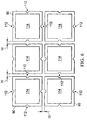
- FIG. 5 illustrates a top view of substrate 90 with shielding layers 114 enclosing the underlying semiconductor die.
- the dicing step removes encapsulant 104 to provide a dicing channel of width D 1 .
- the shielding-lined holes 112 are formed in the dicing channel.
- the singulation D 2 in FIG. 6 through the dicing channel and holes 112 separates the top shielding layer and underlying semiconductor die into individual shielded semiconductor devices.
- FIG. 7 is a perspective view of a shielded semiconductor device with top shielding layer 114 and holes 112 lined with the shielding layer.
- Metal pillars 126 formed in shielding lined holes 112 as shown in FIG. 8 connect top shielding layer 114 to a ground plane embedded in PCB 120 , similar to FIG. 4 .
- FIG. 9 shows an alternate embodiment of the ground connection for the top shielding layer.
- Semiconductor die 130 is electrically connected to substrate 132 using solder bumps 134 .
- Shielding layer 138 overlies encapsulant 140 and blocks EMI, RFI, and other inter-device interference.
- Substrate 132 is mounted to PCB 142 .
- An interconnect structure 144 provides electrical connection between semiconductor die 130 , substrate 132 , and PCB 142 . The individual contacts of interconnect structure 144 are separated by insulating material 146 .
- Substrate 132 has an interconnect structure to electrically connect semiconductor die 130 to PCB 142 .
- a conductive material is deposited into shielding-lined holes 148 to form metal ground pillars 150 which extend into PCB 142 .
- the conductive material for pillars 150 can be Al, Cu, Sn, Ni, Au, or Ag deposited by a PVD, CVD, electrolytic plating, or electroless plating process.
- Metal pillars 150 are configured with hooks 152 which extend over an edge of shielding layer 138 for a mechanically secure connection. Hooks 152 lock shielding layer 138 into place to avoid potential electrical failure due to loss of mechanical contact.
- Metal pillars 150 electrically connect to ground plane 158 which is part of the interconnect structure in PCB 142 . Accordingly, the ground conduction path for shielding layer 138 includes the shielding layer lining of holes 148 , metal pillars 150 , and ground plane 158 of PCB 142 .
- FIG. 10 shows another embodiment of the ground connection for the top shielding layer.
- Semiconductor die 160 is electrically connected to substrate 162 using solder bumps 164 .
- Shielding layer 168 overlies encapsulant 170 and blocks EMI, RFI, and other inter-device interference.
- Substrate 162 is mounted to PCB 172 .
- An interconnect structure 174 provides electrical connection between semiconductor die 160 , substrate 162 , and PCB 172 .
- the individual contacts of interconnect structure 174 are separated by insulating material 176 .
- Substrate 162 has an interconnect structure to electrically connect semiconductor die 160 to PCB 172 .
- the holes 178 are lined with shielding layer 168 .
- a solder material 180 is deposited over the shielding layer lining.
- a conductive material is deposited into a remaining open portion of holes 178 to form metal ground pillars 182 which extend into PCB 172 .
- metal pillars 182 are coated with solder material 180 .
- the conductive material for pillars 182 can be Al, Cu, Sn, Ni, Au, or Ag deposited by a PVD, CVD, electrolytic plating, or electroless plating process.
- Solder material 180 is reflowed to enhance the electrical contact between shielding layer 168 and metal pillars 182 .
- Metal pillars 182 electrically connect to ground plane 184 which is part of the interconnect structure in PCB 172 . Accordingly, the ground conduction path for shielding layer 168 includes the shielding layer lining of holes 178 , solder material 180 , metal pillars 182 , and ground plane 184 of PCB 172 .
- the semiconductor devices are substantially enclosed by a shielding layer using a simple manufacturing process.
- Semiconductor die are mounted to the substrate.
- a top shielding layer is disposed over the semiconductor die.
- a hole is drilled through the semiconductor substrate along a dicing channel between the semiconductor die. The hole is lined with the shielding layer.
- a metal ground pillar is formed in the remaining open portion of the shielding lined hole and electrically connected to a ground plane in the PCB.
- the shielding layer isolates each circuit element from cross-talk generated by adjacent circuit elements.
- the cross-talk may be in the form of conductive coupling, inductive coupling, magnetic field coupling, electric field coupling, or capacitive coupling depending on the electrical nature of the adjacent device.
- the shielded semiconductor device avoids any additional conductive elements in the substrate.
- the substrate can be made thinner as there is no need to alter the circuit design of substrate, nor embed a ground plane in the substrate as found in the prior art.
- the ground plane is disposed in the PCB so it does not impact the structural integrity of the semiconductor substrate.
Abstract
Description
Claims (24)
Priority Applications (1)
| Application Number | Priority Date | Filing Date | Title |
|---|---|---|---|
| US12/136,682 US9123663B2 (en) | 2008-06-10 | 2008-06-10 | Semiconductor device and method of forming shielding layer grounded through metal pillars formed in peripheral region of the semiconductor |
Applications Claiming Priority (1)
| Application Number | Priority Date | Filing Date | Title |
|---|---|---|---|
| US12/136,682 US9123663B2 (en) | 2008-06-10 | 2008-06-10 | Semiconductor device and method of forming shielding layer grounded through metal pillars formed in peripheral region of the semiconductor |
Publications (2)
| Publication Number | Publication Date |
|---|---|
| US20090302436A1 US20090302436A1 (en) | 2009-12-10 |
| US9123663B2 true US9123663B2 (en) | 2015-09-01 |
Family
ID=41399554
Family Applications (1)
| Application Number | Title | Priority Date | Filing Date |
|---|---|---|---|
| US12/136,682 Active 2033-08-22 US9123663B2 (en) | 2008-06-10 | 2008-06-10 | Semiconductor device and method of forming shielding layer grounded through metal pillars formed in peripheral region of the semiconductor |
Country Status (1)
| Country | Link |
|---|---|
| US (1) | US9123663B2 (en) |
Cited By (5)
| Publication number | Priority date | Publication date | Assignee | Title |
|---|---|---|---|---|
| US9412703B1 (en) * | 2015-02-17 | 2016-08-09 | Powertech Technology Inc. | Chip package structure having a shielded molding compound |
| US20170373048A1 (en) * | 2016-04-13 | 2017-12-28 | Taiwan Semiconductor Manufacturing Company, Ltd. | Multi-Die Structure and Method for Forming Same |
| US10163812B2 (en) | 2016-10-19 | 2018-12-25 | Infineon Technologies Ag | Device having substrate with conductive pillars |
| TWI662664B (en) * | 2018-07-31 | 2019-06-11 | 韓商斗星產業股份有限公司 | Magnetic tape for semiconductor fixing |
| US20220122925A1 (en) * | 2019-07-08 | 2022-04-21 | Murata Manufacturing Co., Ltd. | Module and method of manufacturing the same |
Families Citing this family (29)
| Publication number | Priority date | Publication date | Assignee | Title |
|---|---|---|---|---|
| US20060278965A1 (en) * | 2005-06-10 | 2006-12-14 | Foust Donald F | Hermetically sealed package and methods of making the same |
| US20100020518A1 (en) * | 2008-07-28 | 2010-01-28 | Anadigics, Inc. | RF shielding arrangement for semiconductor packages |
| DE102008042449A1 (en) * | 2008-09-29 | 2010-04-01 | Robert Bosch Gmbh | Radar sensor with shielded signal stabilizer |
| TWI381510B (en) * | 2008-10-07 | 2013-01-01 | Advanced Semiconductor Eng | Chip package structure with shielding cover |
| TW201041054A (en) * | 2009-05-11 | 2010-11-16 | Acsip Technology Corp | Electronic component manufacturing method and packaging structure thereof |
| US8084300B1 (en) | 2010-11-24 | 2011-12-27 | Unisem (Mauritius) Holdings Limited | RF shielding for a singulated laminate semiconductor device package |
| TWI452665B (en) * | 2010-11-26 | 2014-09-11 | 矽品精密工業股份有限公司 | Anti-static package structure and fabrication method thereof |
| US8654537B2 (en) * | 2010-12-01 | 2014-02-18 | Apple Inc. | Printed circuit board with integral radio-frequency shields |
| JP5512566B2 (en) | 2011-01-31 | 2014-06-04 | 株式会社東芝 | Semiconductor device |
| TWI491010B (en) * | 2011-03-23 | 2015-07-01 | Universal Scient Ind Shanghai | Miniaturized electromagnetic interference shielding structure and manufacturing method thereof |
| KR20130111780A (en) * | 2012-04-02 | 2013-10-11 | 삼성전자주식회사 | Silicon devices having an emi shield |
| US8952503B2 (en) * | 2013-01-29 | 2015-02-10 | International Business Machines Corporation | Organic module EMI shielding structures and methods |
| US9373583B2 (en) | 2013-03-01 | 2016-06-21 | Qualcomm Incorporated | High quality factor filter implemented in wafer level packaging (WLP) integrated device |
| US9035421B2 (en) * | 2013-03-01 | 2015-05-19 | Qualcomm Incorporated | High quality factor inductor implemented in wafer level packaging (WLP) |
| US9601464B2 (en) | 2014-07-10 | 2017-03-21 | Apple Inc. | Thermally enhanced package-on-package structure |
| US10109593B2 (en) * | 2015-07-23 | 2018-10-23 | Apple Inc. | Self shielded system in package (SiP) modules |
| JP2017050261A (en) * | 2015-09-04 | 2017-03-09 | 富士通株式会社 | Optical module connector and printed board assembly |
| US9930783B2 (en) * | 2016-03-24 | 2018-03-27 | Qualcomm Incorporated | Passive device assembly for accurate ground plane control |
| US10361149B2 (en) * | 2016-08-10 | 2019-07-23 | Qualcomm Incorporated | Land grid array (LGA) packaging of passive-on-glass (POG) structure |
| US10141270B2 (en) * | 2016-12-09 | 2018-11-27 | Amkor Technology, Inc. | Semiconductor device and method of manufacturing thereof |
| US11211340B2 (en) | 2018-11-28 | 2021-12-28 | Shiann-Tsong Tsai | Semiconductor package with in-package compartmental shielding and active electro-magnetic compatibility shielding |
| US10923435B2 (en) | 2018-11-28 | 2021-02-16 | Shiann-Tsong Tsai | Semiconductor package with in-package compartmental shielding and improved heat-dissipation performance |
| US11239179B2 (en) | 2018-11-28 | 2022-02-01 | Shiann-Tsong Tsai | Semiconductor package and fabrication method thereof |
| US10896880B2 (en) | 2018-11-28 | 2021-01-19 | Shiann-Tsong Tsai | Semiconductor package with in-package compartmental shielding and fabrication method thereof |
| TWI744572B (en) * | 2018-11-28 | 2021-11-01 | 蔡憲聰 | Semiconductor package with in-package compartmental shielding and fabrication method thereof |
| CN112117203A (en) * | 2019-10-23 | 2020-12-22 | 中芯集成电路(宁波)有限公司上海分公司 | Packaging method and packaging structure |
| CN113496990B (en) * | 2020-04-01 | 2023-10-20 | 中芯国际集成电路制造(上海)有限公司 | Semiconductor structure and forming method thereof |
| US11587899B2 (en) | 2020-07-29 | 2023-02-21 | Texas Instruments Incorporated | Multi-layer semiconductor package with stacked passive components |
| US20230078862A1 (en) * | 2021-09-13 | 2023-03-16 | Amkor Technology Singapore Holding Pte. Ltd. | Semiconductor devices and methods of manufacturing semiconductor devices |
Citations (14)
| Publication number | Priority date | Publication date | Assignee | Title |
|---|---|---|---|---|
| US5838551A (en) * | 1996-08-01 | 1998-11-17 | Northern Telecom Limited | Electronic package carrying an electronic component and assembly of mother board and electronic package |
| US20020015291A1 (en) * | 1998-07-06 | 2002-02-07 | Hitachi, Ltd. | Semiconductor device |
| US6534859B1 (en) * | 2002-04-05 | 2003-03-18 | St. Assembly Test Services Ltd. | Semiconductor package having heat sink attached to pre-molded cavities and method for creating the package |
| US20040180525A1 (en) * | 2002-01-23 | 2004-09-16 | St Assembly Test Services Ltd. | Heat spreader anchoring and grounding method and thermally enhanced PBGA package using the same |
| US20050067676A1 (en) * | 2003-09-25 | 2005-03-31 | Mahadevan Dave S. | Method of forming a semiconductor package and structure thereof |
| US6881896B2 (en) * | 2003-05-20 | 2005-04-19 | Nec Compound Semiconductor, Ltd. | Semiconductor device package |
| US6947295B2 (en) * | 2003-01-20 | 2005-09-20 | Benq Corporation | Ball grid array package with an electromagnetic shield connected directly to a printed circuit board |
| US20060145361A1 (en) * | 2005-01-05 | 2006-07-06 | Yang Jun Y | Semiconductor device package and manufacturing method thereof |
| US7145084B1 (en) | 2005-08-30 | 2006-12-05 | Freescale Semiconductor, Inc. | Radiation shielded module and method of shielding microelectronic device |
| US7187060B2 (en) | 2003-03-13 | 2007-03-06 | Sanyo Electric Co., Ltd. | Semiconductor device with shield |
| US20070145539A1 (en) | 2005-12-22 | 2007-06-28 | Ken Lam | Method and system for providing an integral radio frequency shield in a molded array package |
| US20080265421A1 (en) * | 2007-04-30 | 2008-10-30 | Infineon Technologies Ag | Structure for Electrostatic Discharge in Embedded Wafer Level Packages |
| US20090294928A1 (en) | 2008-05-28 | 2009-12-03 | Stats Chippac, Ltd. | Semiconductor Device and Method of Forming Holes In Substrate to Interconnect Top Shield and Ground Shield |
| US7687895B2 (en) * | 2007-04-30 | 2010-03-30 | Infineon Technologies Ag | Workpiece with semiconductor chips and molding, semiconductor device and method for producing a workpiece with semiconductors chips |
-
2008
- 2008-06-10 US US12/136,682 patent/US9123663B2/en active Active
Patent Citations (14)
| Publication number | Priority date | Publication date | Assignee | Title |
|---|---|---|---|---|
| US5838551A (en) * | 1996-08-01 | 1998-11-17 | Northern Telecom Limited | Electronic package carrying an electronic component and assembly of mother board and electronic package |
| US20020015291A1 (en) * | 1998-07-06 | 2002-02-07 | Hitachi, Ltd. | Semiconductor device |
| US20040180525A1 (en) * | 2002-01-23 | 2004-09-16 | St Assembly Test Services Ltd. | Heat spreader anchoring and grounding method and thermally enhanced PBGA package using the same |
| US6534859B1 (en) * | 2002-04-05 | 2003-03-18 | St. Assembly Test Services Ltd. | Semiconductor package having heat sink attached to pre-molded cavities and method for creating the package |
| US6947295B2 (en) * | 2003-01-20 | 2005-09-20 | Benq Corporation | Ball grid array package with an electromagnetic shield connected directly to a printed circuit board |
| US7187060B2 (en) | 2003-03-13 | 2007-03-06 | Sanyo Electric Co., Ltd. | Semiconductor device with shield |
| US6881896B2 (en) * | 2003-05-20 | 2005-04-19 | Nec Compound Semiconductor, Ltd. | Semiconductor device package |
| US20050067676A1 (en) * | 2003-09-25 | 2005-03-31 | Mahadevan Dave S. | Method of forming a semiconductor package and structure thereof |
| US20060145361A1 (en) * | 2005-01-05 | 2006-07-06 | Yang Jun Y | Semiconductor device package and manufacturing method thereof |
| US7145084B1 (en) | 2005-08-30 | 2006-12-05 | Freescale Semiconductor, Inc. | Radiation shielded module and method of shielding microelectronic device |
| US20070145539A1 (en) | 2005-12-22 | 2007-06-28 | Ken Lam | Method and system for providing an integral radio frequency shield in a molded array package |
| US20080265421A1 (en) * | 2007-04-30 | 2008-10-30 | Infineon Technologies Ag | Structure for Electrostatic Discharge in Embedded Wafer Level Packages |
| US7687895B2 (en) * | 2007-04-30 | 2010-03-30 | Infineon Technologies Ag | Workpiece with semiconductor chips and molding, semiconductor device and method for producing a workpiece with semiconductors chips |
| US20090294928A1 (en) | 2008-05-28 | 2009-12-03 | Stats Chippac, Ltd. | Semiconductor Device and Method of Forming Holes In Substrate to Interconnect Top Shield and Ground Shield |
Cited By (8)
| Publication number | Priority date | Publication date | Assignee | Title |
|---|---|---|---|---|
| US9412703B1 (en) * | 2015-02-17 | 2016-08-09 | Powertech Technology Inc. | Chip package structure having a shielded molding compound |
| US20170373048A1 (en) * | 2016-04-13 | 2017-12-28 | Taiwan Semiconductor Manufacturing Company, Ltd. | Multi-Die Structure and Method for Forming Same |
| US10553569B2 (en) * | 2016-04-13 | 2020-02-04 | Taiwan Semiconductor Manufacturing Company, Ltd. | Multi-die structure and method for forming same |
| US10163812B2 (en) | 2016-10-19 | 2018-12-25 | Infineon Technologies Ag | Device having substrate with conductive pillars |
| US10304780B2 (en) | 2016-10-19 | 2019-05-28 | Infineon Technologies Ag | Device having substrate with conductive pillars |
| TWI662664B (en) * | 2018-07-31 | 2019-06-11 | 韓商斗星產業股份有限公司 | Magnetic tape for semiconductor fixing |
| US20220122925A1 (en) * | 2019-07-08 | 2022-04-21 | Murata Manufacturing Co., Ltd. | Module and method of manufacturing the same |
| US11837555B2 (en) * | 2019-07-08 | 2023-12-05 | Murata Manufacturing Co., Ltd. | Module and method of manufacturing the same |
Also Published As
| Publication number | Publication date |
|---|---|
| US20090302436A1 (en) | 2009-12-10 |
Similar Documents
| Publication | Publication Date | Title |
|---|---|---|
| US9123663B2 (en) | Semiconductor device and method of forming shielding layer grounded through metal pillars formed in peripheral region of the semiconductor | |
| US8598690B2 (en) | Semiconductor device having conductive vias in peripheral region connecting shielding layer to ground | |
| US7851893B2 (en) | Semiconductor device and method of connecting a shielding layer to ground through conductive vias | |
| US9543258B2 (en) | Semiconductor device and method of forming holes in substrate to interconnect top shield and ground shield | |
| US7880275B2 (en) | Semiconductor device and method of forming shielding along a profile disposed in peripheral region around the device | |
| US10388612B2 (en) | Semiconductor device and method of forming electromagnetic (EM) shielding for LC circuits | |
| US9401347B2 (en) | Semiconductor device and method of forming a shielding layer over a semiconductor die disposed in a cavity of an interconnect structure and grounded through the die TSV | |
| US8076757B2 (en) | Semiconductor device having electrical devices mounted to IPD structure and method of shielding electromagnetic interference | |
| US8648448B2 (en) | Semiconductor device and method of shielding semiconductor die from inter-device interference | |
| US9236352B2 (en) | Semiconductor die and method of forming noise absorbing regions between THVs in peripheral region of the die | |
| KR101769995B1 (en) | semiconductor device and method of forming shielding layer after encapsulation and grounded through interconnect structure | |
| US9406619B2 (en) | Semiconductor device including pre-fabricated shielding frame disposed over semiconductor die | |
| US9437482B2 (en) | Semiconductor device and method of forming shielding layer over active surface of semiconductor die | |
| US20110309892A1 (en) | Semiconductor Device and Method of Integrating Balun and RF Coupler on a Common Substrate | |
| US9190340B2 (en) | Semiconductor device and method of forming RF FEM and RF transceiver in semiconductor package | |
| US9082638B2 (en) | Semiconductor device with cross-talk isolation using M-cap |
Legal Events
| Date | Code | Title | Description |
|---|---|---|---|
| AS | Assignment |
Owner name: STATS CHIPPAC, LTD., SINGAPORE Free format text: ASSIGNMENT OF ASSIGNORS INTEREST;ASSIGNORS:KIM, OHHAN;KIM, SEUNGWON;PARK, JOUNGUN;REEL/FRAME:021075/0232 Effective date: 20080604 |
|
| AS | Assignment |
Owner name: CITICORP INTERNATIONAL LIMITED, AS COMMON SECURITY AGENT, HONG KONG Free format text: SECURITY INTEREST;ASSIGNORS:STATS CHIPPAC, INC.;STATS CHIPPAC LTD.;REEL/FRAME:036288/0748 Effective date: 20150806 Owner name: CITICORP INTERNATIONAL LIMITED, AS COMMON SECURITY Free format text: SECURITY INTEREST;ASSIGNORS:STATS CHIPPAC, INC.;STATS CHIPPAC LTD.;REEL/FRAME:036288/0748 Effective date: 20150806 |
|
| STCF | Information on status: patent grant |
Free format text: PATENTED CASE |
|
| AS | Assignment |
Owner name: STATS CHIPPAC PTE. LTE., SINGAPORE Free format text: CHANGE OF NAME;ASSIGNOR:STATS CHIPPAC LD.;REEL/FRAME:038378/0442 Effective date: 20160329 |
|
| AS | Assignment |
Owner name: STATS CHIPPAC PTE. LTD., SINGAPORE Free format text: CORRECTIVE ASSIGNMENT TO CORRECT THE ASSIGNOR NAME PREVIOUSLY RECORDED AT REEL: 039514 FRAME: 0451. ASSIGNOR(S) HEREBY CONFIRMS THE CHANGE OF NAME;ASSIGNOR:STATS CHIPPAC LTD.;REEL/FRAME:039980/0838 Effective date: 20160329 |
|
| MAFP | Maintenance fee payment |
Free format text: PAYMENT OF MAINTENANCE FEE, 4TH YEAR, LARGE ENTITY (ORIGINAL EVENT CODE: M1551); ENTITY STATUS OF PATENT OWNER: LARGE ENTITY Year of fee payment: 4 |
|
| AS | Assignment |
Owner name: STATS CHIPPAC, INC., CALIFORNIA Free format text: RELEASE BY SECURED PARTY;ASSIGNOR:CITICORP INTERNATIONAL LIMITED, AS COMMON SECURITY AGENT;REEL/FRAME:053476/0094 Effective date: 20190503 Owner name: STATS CHIPPAC PTE. LTD. FORMERLY KNOWN AS STATS CHIPPAC LTD., SINGAPORE Free format text: RELEASE BY SECURED PARTY;ASSIGNOR:CITICORP INTERNATIONAL LIMITED, AS COMMON SECURITY AGENT;REEL/FRAME:053476/0094 Effective date: 20190503 |
|
| MAFP | Maintenance fee payment |
Free format text: PAYMENT OF MAINTENANCE FEE, 8TH YEAR, LARGE ENTITY (ORIGINAL EVENT CODE: M1552); ENTITY STATUS OF PATENT OWNER: LARGE ENTITY Year of fee payment: 8 |