US9123501B2 - Device for correcting diffraction aberration of electron beam - Google Patents
Device for correcting diffraction aberration of electron beam Download PDFInfo
- Publication number
- US9123501B2 US9123501B2 US13/977,139 US201113977139A US9123501B2 US 9123501 B2 US9123501 B2 US 9123501B2 US 201113977139 A US201113977139 A US 201113977139A US 9123501 B2 US9123501 B2 US 9123501B2
- Authority
- US
- United States
- Prior art keywords
- charged particle
- diffraction
- diffraction aberration
- electron beam
- sample
- Prior art date
- Legal status (The legal status is an assumption and is not a legal conclusion. Google has not performed a legal analysis and makes no representation as to the accuracy of the status listed.)
- Expired - Fee Related
Links
Images


Classifications
-
- H—ELECTRICITY
- H01—ELECTRIC ELEMENTS
- H01J—ELECTRIC DISCHARGE TUBES OR DISCHARGE LAMPS
- H01J37/00—Discharge tubes with provision for introducing objects or material to be exposed to the discharge, e.g. for the purpose of examination or processing thereof
- H01J37/02—Details
- H01J37/04—Arrangements of electrodes and associated parts for generating or controlling the discharge, e.g. electron-optical arrangement, ion-optical arrangement
- H01J37/10—Lenses
-
- H—ELECTRICITY
- H01—ELECTRIC ELEMENTS
- H01J—ELECTRIC DISCHARGE TUBES OR DISCHARGE LAMPS
- H01J37/00—Discharge tubes with provision for introducing objects or material to be exposed to the discharge, e.g. for the purpose of examination or processing thereof
- H01J37/02—Details
- H01J37/04—Arrangements of electrodes and associated parts for generating or controlling the discharge, e.g. electron-optical arrangement, ion-optical arrangement
- H01J37/147—Arrangements for directing or deflecting the discharge along a desired path
-
- H—ELECTRICITY
- H01—ELECTRIC ELEMENTS
- H01J—ELECTRIC DISCHARGE TUBES OR DISCHARGE LAMPS
- H01J37/00—Discharge tubes with provision for introducing objects or material to be exposed to the discharge, e.g. for the purpose of examination or processing thereof
- H01J37/02—Details
- H01J37/04—Arrangements of electrodes and associated parts for generating or controlling the discharge, e.g. electron-optical arrangement, ion-optical arrangement
- H01J37/153—Electron-optical or ion-optical arrangements for the correction of image defects, e.g. stigmators
-
- H—ELECTRICITY
- H01—ELECTRIC ELEMENTS
- H01J—ELECTRIC DISCHARGE TUBES OR DISCHARGE LAMPS
- H01J37/00—Discharge tubes with provision for introducing objects or material to be exposed to the discharge, e.g. for the purpose of examination or processing thereof
- H01J37/26—Electron or ion microscopes; Electron or ion diffraction tubes
-
- H—ELECTRICITY
- H01—ELECTRIC ELEMENTS
- H01J—ELECTRIC DISCHARGE TUBES OR DISCHARGE LAMPS
- H01J2237/00—Discharge tubes exposing object to beam, e.g. for analysis treatment, etching, imaging
- H01J2237/153—Correcting image defects, e.g. stigmators
- H01J2237/1534—Aberrations
-
- H—ELECTRICITY
- H01—ELECTRIC ELEMENTS
- H01J—ELECTRIC DISCHARGE TUBES OR DISCHARGE LAMPS
- H01J2237/00—Discharge tubes exposing object to beam, e.g. for analysis treatment, etching, imaging
- H01J2237/26—Electron or ion microscopes
- H01J2237/2614—Holography or phase contrast, phase related imaging in general, e.g. phase plates
Definitions
- the present invention relates to a technique for manufacturing a substrate having a fine circuit pattern, such as a semiconductor device, a liquid crystal, and a magnetic recording medium, and in particular, to a charged particle beam microscope and an inspection method for observing, measuring, and inspecting a fine circuit pattern using a charged particle beam.
- a fine circuit pattern such as a semiconductor device, a liquid crystal, and a magnetic recording medium
- the miniaturization of a circuit pattern is going on in the management or development of the manufacturing process, so that the size of a hole or a groove formed on the wafer is about 10 nm in the case of a fine hole or groove. For this reason, demands for measuring a fine pattern having a size of tens of nanometers with high accuracy and at high speed are increasing more and more.
- the probe diameter of the electron beam of a scanning electron microscope (hereinafter, referred to as an SEM) has been reduced year by year to about nm.
- This SEM is a high-resolution observation image acquisition means next to a scanning probe microscope (hereinafter, referred to as an SPM) having atomic resolution.
- a critical dimension scanning electron microscope (hereinafter, referred to as a CD-SEM) is an essential measuring apparatus in semiconductor lithography management, but the damage to the resist by the electron beam is an obstacle to measurement.
- measurement at 100 eV or less has been proposed.
- electron beam of ultra-low acceleration voltage is required for low damage observation of soft materials.
- the optical aberration correction is an aberration caused geometrically and optically by a lens or the like of the electron optical system, and has a feature that the aberration increases as the opening angle of the beam on a sample increases.
- the diffraction aberration is an aberration caused by the wave nature of electrons, and has a feature that the aberration increases as the opening angle of the beam on a sample decreases. Assuming that the allowable range of the sample height at which the resolution is degraded by 10% is the depth of focus of an observation image, the depth of focus increases as the beam opening angle on the sample decreases.
- NPL 1 discloses a method of correcting a chromatic aberration, among optical aberrations, by creating the straight-through condition of Wien filters by multiple poles when the electric field and the magnetic field are superimposed.
- PTL 1 discloses a scanning charged particle beam microscope characterized in that a passage opening to restrict the passage of a charged particle beam is disposed between a charged particle source and a scanning deflector and the passage opening includes a member, which restricts the passage of a charged particle beam, at the center of the opening.
- PTL 2 discloses a method for realizing stable beam extraction by arranging a solenoid coil and a magnet array in the ion source plasma chamber and confining the plasma so that the magnetic field strength is minimum in a central plasma portion on the average in both the axial direction and the radial direction when the combined magnetic field shape is seen from the plasma side.
- PTL 3 discloses a magnet in which auxiliary coils for adjusting the balance, which are independent of and adjacent to main coils, are wound in a solenoid shape with pole pieces of the upper and lower portions interposed therebetween and which generates a magnetic field in a pole piece gap.
- a transmission electron microscope hereinafter, referred to as a TEM
- a scanning transmission electron microscope hereinafter, referred to as an STEM
- the spherical aberration and the chromatic aberration have been dominant factors in the resolution degradation. That is, since the spherical aberration has been a dominant factor rather than the chromatic aberration in the STEM or the TEM and the chromatic aberration has been a dominant factor rather than the spherical aberration in the SEM, optical aberration correction techniques optimized for the respective microscopes have been developed. By the appearance of these optical aberration correction techniques, aberrations of the entire optical system are suppressed, and a diffraction aberration is now a dominant factor in the resolution degradation as a common feature of the structures of the optical systems.
- the optical aberration can be corrected, but the diffraction aberration cannot be corrected. Since the optical aberration correction has a feature that the aberration increases as the opening angle of the beam on a sample increases and the diffraction aberration has a feature that the aberration increases as the opening angle of the beam decreases, it is possible to suppress the aberration by the optical aberration correction if the opening angle of the beam is increased. If the opening angle of the beam is increased, the depth of focus may become shallow. As a result, the top surface or the bottom of a groove or a hole on the sample may not be able to be observed simultaneously, or detection of the in-focus position may become difficult. The observation image with shallow depth of focus becomes an inconvenient observation image, with which it is difficult to obtain three-dimensional information, compared with a conventional SEM image.
- the energy filter of the electron microscope can be realized by arranging the magnet that generates a magnetic field in a pole piece gap by winding coils in a solenoid shape with pole pieces of the upper and lower portions interposed therebetween, but the diffraction aberration of an electron beam cannot be corrected.
- the wave nature of electrons becomes strong.
- the phenomenon of spot form expansion of the beam on a sample by the above diffraction is the Rayleigh diffraction.
- the intensity distribution of the diffracted wave on the sample changes due to the phase difference within the beam diameter caused by the traveling direction of the electron beam.
- the intensity distribution of the diffracted wave on the sample is attenuated.
- the wavelength of the electron beam is increased, a phase difference within the beam diameter according to the traveling direction is less likely to occur. Accordingly, attenuation of the intensity distribution of the diffracted wave becomes weak. For this reason, the diffraction aberration increases as the acceleration level becomes low.
- AB effect used for phase control of the electron beam
- the Rayleigh diffraction can be suppressed by efficiently causing a phase difference within the beam diameter by the inclination of the traveling direction of the electron beam from the beam axis. Therefore, in order to cause the above-described phase difference, a diffraction aberration corrector that induces a vector potential, which is perpendicular to the beam axis and has a symmetrical distribution within the orthogonal plane, is provided between the objective aperture and the objective lens.
- the intensity of the electron beam on the sample does not change without a change in the phase difference of the electron beam traveling along the beam axis.
- a diffracted wave which travels in a state of being inclined from the beam axis due to Fresnel diffraction on the electron beam path, increases the phase difference within the beam diameter by the AB effect due to the vector potential. As a result, it is possible to suppress the intensity of the electron beam on the sample.
- the electron beam focused on the sample by the objective lens travels while causing a diffracted wave.
- the phenomenon of spot form expansion of the beam on the sample by the above diffraction is the Rayleigh diffraction.
- the intensity distribution of the diffracted wave on the sample changes due to the phase difference within the beam diameter caused by the focusing direction of the electron beam.
- the intensity distribution of the diffracted wave on the sample is attenuated with an amplitude variation. It is difficult to cause a phase difference within the beam diameter efficiently for the electron beam focused by the objective lens. Therefore, for a diffracted wave of the electron beam before passing through the objective lens, a phase difference from the beam axis is efficiently caused by the inclination from the beam axis. In this case, since a phase difference between diffracted waves before and after the objective lens occurs, it is possible to suppress the Rayleigh diffraction.
- a desired vector potential distribution can be obtained by arranging the solenoid coil rings or the magnet rings at the positions on the same circumference around the beam axis, which are symmetrical with respect to the beam axis, so that the extension direction of the ring surface faces the beam axis.
- the above is realized by arranging a pair of solenoid coil rings so that the extension direction of two ring surfaces disposed at the symmetrical positions crosses the beam axis and the induced vector potential is rotationally symmetrical with respect to the beam axis and also arranging another pair of solenoid coil rings at the positions, at which the relative angles are 90°, so that the directions of the vector potentials of the pair of solenoid coil rings are rotationally symmetrical and the directions of the vector potentials of the adjacent solenoid coil rings are axisymmetrical.
- rotational symmetry of the vector potential becomes better by using solenoid coil rings of a multiple of 4, such as 8 or 12, on the same circumference around the beam axis.
- the rotational symmetry of the vector potential becomes better by forming a ring rotating around the beam axis with a cylinder obtained by spirally winding the solenoid coil.
- the present invention in the charged particle beam microscope to observe, measure, and inspect a fine circuit pattern using a charged particle beam, it is possible to suppress the diffraction aberration on the sample by increasing the phase difference within the beam diameter of the vector potential.
- FIG. 1 is a diagram showing an embodiment in which a diffraction aberration corrector is applied to a scanning electron microscope.
- FIG. 2 is a schematic diagram of the diffraction aberration in the scanning electron microscope.
- FIG. 3 is an explanatory view of the Aharanov-Bohm effect.
- FIG. 4 is a schematic diagram showing a method of correcting the aberration due to Rayleigh diffraction.
- FIG. 5A is a diagram showing a specific method of correcting the Rayleigh diffraction.
- FIG. 5B is an enlarged view of a diffraction aberration corrector.
- FIG. 6 is a diagram showing the beam intensity distribution on a sample.
- FIG. 7 is a diagram showing an example of the arrangement of poles of the vector potential of the diffraction aberration corrector.
- FIG. 8 is a diagram showing an example of the control screen of the diffraction aberration corrector.
- FIG. 9 is a diagram showing an embodiment in which the diffraction aberration corrector is applied to an ion microscope.
- FIG. 10 is a diagram showing an embodiment in which the diffraction aberration corrector is applied to a transmission electron microscope.
- FIG. 11 is a diagram showing an embodiment in which the diffraction aberration corrector is applied to a reflection electron microscope.
- FIG. 12 is a diagram showing an embodiment in which the diffraction aberration corrector is applied to a mirror electron microscope.
- an example of application of apparatus using a scanning electron microscope will be described.
- means for correcting the diffraction aberration in each embodiment can be generally applied to charged particle beam apparatuses including not only an electron beam apparatus but also an ion beam apparatus.
- an apparatus having a semiconductor wafer as a sample will be described.
- samples used in various kinds of charged particle beam apparatuses not only the semiconductor wafer but also various kinds of samples, such as a semiconductor substrate, a fragment of a wafer on which a pattern is formed, a chip cut out from the wafer, a hard disk, and a liquid crystal panel, can be inspected and measured.
- the scanning electron microscope of the present embodiment is configured to include an electron optical system formed in the vacuum housing, an electron optical system control device disposed around the electron optical system, a host computer that performs overall control of the entire apparatus by controlling each control unit included in a control power supply, a console connected to the control device, and display means including a monitor that displays an acquired image.
- the electron optical system control device is formed by a power supply unit for supplying a current and a voltage to each component of the electron optical system, a signal control line for transmitting a control signal to each component, and the like.
- the scanning electron microscope is set as an example of an application. However, the present invention may also be applied to an ion microscope, a transmission electron microscope, a reflection electron microscope, or a mirror electron microscope, for example.
- FIG. 1 is a schematic diagram showing the overall configuration of the scanning electron microscope of the present invention.
- the scanning electron microscope of the present embodiment is configured to include an electron optical system 102 formed in a vacuum housing 101 , an electron optical system control device 103 disposed around the electron optical system 102 , a host computer 104 that performs overall control of the entire apparatus by controlling each control unit included in a control power supply, a console 105 connected to the control device, and display means 106 including a monitor that displays an acquired image.
- the electron optical system control device 103 is formed by a power supply unit for supplying a current and a voltage to each component of the electron optical system 102 , a signal control line for transmitting a control signal to each component, and the like.
- the host computer 104 that performs overall control of the entire apparatus may be of any type.
- the host computer 104 may be connected to a communication system or a system that transports a wafer as a sample to be observed from the wafer storage cassette to the sample chamber.
- the electron optical system 102 is configured to include an electron source 111 that generates an electron beam 110 , an objective aperture 112 that limits the beam diameter of the electron beam 110 , an aberration corrector 113 that controls the optical aberration of the electron beam 110 , a diffraction aberration corrector 114 that controls the diffraction aberration of the electron beam 110 , a deflector 115 that deflects the primary electron beam, a combined immersion lens of magnetic field and electrostatic field 116 that focuses the electron beam 110 , a booster magnetic path member 119 that focuses and diverges a secondary particle 118 , which is emitted from a sample 117 held on the stage, a reflecting member 120 with which the secondary particle 118 collides, and a central detector 122 that detects a third particle 121 re-emitted by the collision.
- the reflecting member 120 is formed by a disc-shaped metal member in which an opening, through which the electron beam 110 passes, is formed, and the bottom surface forms a secondary particle reflecting surface.
- the electron beam 110 emitted from the electron source 111 is accelerated by the potential difference formed between an extraction electrode 130 and an acceleration electrode 131 and reaches the combined immersion lens of magnetic field and electrostatic field 116 .
- the combined immersion lens of magnetic field and electrostatic field 116 focuses the incident electron beam 110 by exciting the magnetic field on the sample 117 using a coil 132 .
- a negative electric potential with respect to the electric potential of a yoke member 134 is supplied to a control magnetic path member 133 , and this electric potential is supplied by a control magnetic path power supply 135 .
- an electric potential is applied to a stage 136 by a stage power supply 137 so that the potential difference between this electric potential and the electric potential of the booster magnetic path member 119 becomes negative.
- the electron beam 110 having passed through the booster magnetic path member 119 is abruptly decelerated to reach the sample surface.
- the landing energy of the electron beam 110 is determined only by the potential difference between the electron source 111 and the stage 136 , if the electric potential applied to the electron source 111 and the stage 136 is controlled to have a predetermined value, the landing energy of the electron beam 110 can be controlled to be a desired value regardless of the electric potential applied to the booster magnetic path member 119 or the acceleration electrode 131 .
- the combined immersion lens of magnetic field and electrostatic field 116 may be of any type. For example, it may be the combined immersion lens of magnetic field and electrostatic field 116 without the control magnetic path member 133 , a magnetic lens, or an electrostatic lens.
- poles of vector potentials formed by the cylindrical pipe to form a solenoid coil in a doughnut-shaped ring or a solenoid coil ring are disposed at the positions on the same circumference around the beam axis, which are symmetrical with respect to the beam axis of the electron beam 110 having passed the objective aperture 112 , so that the extension direction of the surface of the solenoid coil ring crosses the beam axis, another pair of poles of vector potentials are disposed at the positions, at which the relative angles with respect to the poles of the two vector potentials are 90° so that the extension direction of the surface of the solenoid coil ring crosses the beam axis, and the ring direction of the magnetic flux induced in the solenoid coil by the pair of poles of each vector potential is set so as to be rotationally symmetrical with respect to the beam axis and the ring direction of the magnetic flux induced in the solenoid coil by the poles of the adjacent vector potential is set so as to
- the configuration of the multipole of the vector potential of the diffraction aberration corrector 114 may be an octapole, 12-pole, or consecutive pole other than the quadrupole.
- the pole of the vector potential may be a magnet ring or the like other than the solenoid coil.
- a condenser lens may be provided in the diffraction aberration corrector 114 .
- Any type of optical aberration corrector 113 may be used as long as it is a device for correcting the optical aberration of the electron beam 110 .
- the optical aberration corrector 113 is formed by multiple poles of a magnetic pole and an electrode and a condenser lens.
- FIG. 2 is a schematic diagram of the diffraction aberration in a scanning electron microscope. Although there are Rayleigh diffraction caused by Fresnel diffraction, wavefront aberration, and the like in the diffraction aberration, the characteristics of the aberration and the aberration correction method in the Rayleigh diffraction will be described below in the present invention.
- the intensity distribution of the diffracted wave on the sample is attenuated with an amplitude variation due to the Rayleigh diffraction 216 since it changes due to the phase difference within the beam diameter 217 of the electron beam 212 as the inclination of the focusing direction of the electron beam from the axis of the beam increases.
- the beam landing speed of the electron beam 212 becomes a low speed, the wavelength of the electron wave becomes long. Accordingly, since a phase difference within the beam diameter of the diffracted wave caused by the Fresnel diffraction 215 is difficult to occur, attenuation due to diffraction angle of the intensity distribution of the diffracted wave becomes weak. For this reason, the Rayleigh diffraction 216 increases as the acceleration level becomes low.
- the electron beam 212 travels while generating the diffracted wave due to the Fresnel diffraction 215 .
- the Rayleigh diffraction 216 is also a phenomenon causing the spot shape expansion of the beam on the sample 211 by interference between the diffracted wave generated on the path of the electron beam 212 up to the objective lens 210 and the diffracted wave generated on the focusing orbit of the electron beam 212 by the objective lens 210 .
- FIG. 3 is an explanatory view of the AB effect used in the phase control of the electron beam.
- the method of demonstrating the AB effect using the technique of an electron beam holography is a method of observing an interference fringe 314 of an electron beam 311 on a sample 313 using an electron beam control device that divides the electron beam 311 emitted from an electron source 310 into two orbits and focuses the electron beam on the sample 313 after passing through both the sides with a sufficiently long solenoid coil 312 interposed therebetween.
- a current 315 is made to flow through the solenoid coil 312 , a magnetic field can be induced only in the solenoid coil.
- the solenoid coil 310 When demonstrating the AB effect, it is difficult to satisfy the condition, in which no magnetic field or electric field is present, in the solenoid coil 310 with a limited length. For this reason, it has been necessary to suppress the magnetic field leakage by forming the solenoid coil in a donut-shaped ring and make the solenoid coil very fine (several micrometers) because the wavelength of the electron beam is extremely short.
- the magnet of a very fine ring was surrounded with a superconducting material so that the leakage of the magnetic field of the magnet was completely prevented by the Meissner effect, and the phase difference between electron beams passing through the inner and outer sides of the ring was observed in the form of interference fringes using electron beam holography. As a result of the observation, it was found that there was a phase difference of only a half wavelength between the orbits of two electron beams, and it was demonstrated that the phase of the electron beam was changed by the vector potential.
- FIG. 4 is a schematic diagram showing a method of correcting the aberration due to Rayleigh diffraction.
- Rayleigh diffraction 410 is a phenomenon causing the spot shape expansion of the beam on a sample 409 by interference between a diffracted wave 413 generated on the path of an electron beam 412 up to an objective lens 411 and a diffracted wave 414 generated on the focusing orbit of the electron beam 412 by the objective lens 411 .
- the electron beam 412 from the objective aperture 415 to the objective lens 411 is a collimated beam whose optical orbit is controlled by a condenser lens 416 or the like, and the phase of the electron beam is a plane wave.
- the phase difference within the beam diameter of the diffracted wave 413 generated up to the objective lens 411 increases depending on the inclination of the traveling direction of the electron beam from the beam axis.
- a diffraction aberration corrector 417 that induces a vector potential, which is perpendicular to the beam axis and has a symmetrical distribution within the orthogonal plane, is provided between the objective aperture 415 and the objective lens 411 . Since the path integral to take an inner product between the electron beam 412 , which travels along the beam axis, and the vector potential becomes 0 when the electron beam 412 passes through the diffraction aberration corrector 417 , the phase is not changed by the AB effect. Accordingly, even if the electron beam 412 is focused on the sample 409 by the objective lens 411 , the beam intensity does not change.
- the path integral to take an inner product between the diffracted wave 413 , which travels in a state of being inclined from the beam axis due to Fresnel diffraction 418 , and the vector potential does not become 0. Accordingly, a phase difference may be caused by the AB effect.
- the path integral difference is increased by the distribution of the vector potential within the beam diameter, the phase difference within the beam diameter is increased, and accordingly the Rayleigh diffraction 410 on the sample 409 can be suppressed.
- the electron beam travels while generating the diffracted wave 414 .
- the Rayleigh diffraction 410 which is a phenomenon of spot shape expansion of the beam on the sample 409 , remains due to the diffracted wave 414 . That is, the intensity distribution of the diffracted wave on the sample 409 changes due to the phase difference within the beam diameter caused by the focusing direction of the electron beam 412 .
- the diffracted wave of the electron beam 412 on the sample becomes an interference wave between the diffracted wave 414 , which is caused by the Fresnel diffraction 418 on the path of the electron beam 412 from the objective aperture 415 to the diffraction aberration corrector 417 , and a diffracted wave, which is caused by the Fresnel diffraction 418 on the path of the electron beam 412 until the electron beam 412 passes through the diffraction aberration corrector 417 to the objective lens 411 and is focused on the sample 409 .
- the above-described interference wave may have a sharp peak shape.
- FIGS. 5A and 5B show a specific method of correcting the Rayleigh diffraction.
- a diffraction aberration corrector 510 can induce a vector potential 512 that is parallel to the beam axis of an electron beam 511 and has a symmetrical distribution within the orthogonal plane.
- An example of the configuration of a scanning electron microscope 515 in which the diffraction aberration corrector 510 is provided will be described below.
- the diffraction aberration corrector 510 is provided between the objective aperture 513 and the objective lens 514 .
- an aberration corrector that corrects the optical aberration such as a chromatic aberration or a spherical aberration
- a deflector is placed between the objective lens 514 and the sample 522 , it is also possible to superimpose the objective lens 514 and the diffraction aberration corrector 510 .
- the diffraction aberration corrector 510 induces not only the vector potential induced by the magnetic flux in the solenoid coil but also the vector potential by the ring of the magnetic flux leaking from the solenoid coil to the beam axis.
- the vector potential induced by the magnetic flux in the solenoid coil ring does not cause a phase difference as long as the electron beam 511 does not cross the solenoid coil.
- the vector potential induced in the ring of the leaking magnetic flux forms a quadrupole, and induces a vector potential distribution that is symmetrical along the beam axis and is also symmetrical with respect to the beam axis.
- the distribution of the vector potential within a plane perpendicular to the beam axis is the distribution that is symmetrical with respect to the beam axis.
- the polar coordinates within the orthogonal plane with respect to the beam axis are assumed to be [Expression 1].
- ⁇ right arrow over (r) ⁇ ( r cos( ⁇ ), r sin( ⁇ )) [Expression 1]
- ⁇ ⁇ ( r ⁇ , R ⁇ ) ⁇ 2 ⁇ ⁇ ⁇ ⁇ ⁇ a ⁇ r ⁇ ⁇ R ⁇ + 2 ⁇ ⁇ ⁇ ⁇ e ⁇ ⁇ ⁇ ha ⁇ ⁇ d s ⁇
- (Expression 7) is the coordinates of the sample 521
- a is a beam opening angle 526 on a sample.
- the wave function of the electron beam 511 on the sample is (Expression 8).
- ⁇ is a wavelength of the electron beam 511
- J 1 ( ) and J 0 ( ) are Bessel functions.
- Rayleigh diffraction 527 of the electron beam 511 on the sample 521 becomes an interference wave between the first diffracted wave 529 of (Expression 8) caused by the Fresnel diffraction 528 on the first path of the electron beam 511 from the objective aperture 513 to the diffraction aberration corrector 510 and a second diffracted wave 531 caused by Fresnel diffraction 530 on the second path of the electron beam 511 until the electron beam 511 passes through the diffraction aberration corrector 510 to the objective lens 514 and is focused on the sample 521 .
- the wave function of the Rayleigh diffraction 527 of the electron beam 511 on the sample is (Expression 9).
- L C is a normalization factor of the first diffracted wave 529 caused by the Fresnel diffraction 528 on the first path of the electron beam 511 from the objective aperture 513 to the diffraction aberration corrector 510
- L F is a normalization factor of the second diffracted wave 531 caused by the Fresnel diffraction 530 on the second path of the electron beam 511 until the electron beam 511 passes through the diffraction aberration corrector 510 to the objective lens 514 and is focused on the sample 521 .
- the wave function of conventional Rayleigh diffraction 532 when there is no diffraction aberration corrector is [Expression 10].
- L is a normalization factor
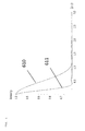
- FIG. 6 is a diagram showing the beam intensity distribution on a sample.
- the square of the wave function (Expression 9) of the Rayleigh diffraction of the electron beam on the sample is a beam intensity distribution 611 after diffraction aberration correction.
- the square of the wave function (Expression 10) of the conventional Rayleigh diffraction when there is no diffraction aberration corrector is a beam intensity distribution 610 before diffraction aberration correction.
- the horizontal axis is an axis scaled by the wavelength of the electron beam and the beam opening angle on the sample when the distance from the beam axis on the sample is assumed to be r.
- a point crossing the horizontal axis at 0.61 D is a point indicating the Rayleigh resolution which is a basic characteristic of the diffraction aberration.
- the interference wave may have a sharp peak shape, compared with the Rayleigh diffraction when there is no diffraction aberration corrector.
- the shape of the beam intensity distribution becomes a sharp peak if A′′ is appropriately set.
- FIG. 7 is an example of the arrangement of poles of the vector potential of a diffraction aberration corrector.
- This is an example of the arrangement of a cylindrical pipe to form a solenoid coil with a doughnut-shaped ring or a solenoid coil ring or a pair of poles of the vector potential formed by a pair of magnet rings or the like.
- a quadrupole 710 of the vector potential is adopted in the above-described embodiment, it is possible to suppress the spread of the vector potential in a beam axis direction by setting an octapole 712 , 12-pole, and 16-pole of the vector potential.
- a consecutive pole 713 of the vector potential to form a ring rotating around the beam axis with a cylinder obtained by spirally winding the solenoid coil is used, rotational symmetry of the vector potential becomes better.
- FIG. 8 is an example of a control screen of a diffraction aberration corrector. This is formed by a screen 810 that displays the axis control value of the multipole of the vector potential for each combination of acceleration of the electron beam, current, and the opening angle at the time of beam focusing, a screen 811 to measure or register the axis control value, a screen 812 indicating the alignment of multiple poles of the vector potential, and the like.
- FIG. 9 is an example in which the diffraction aberration corrector is applied to an ion microscope.
- Rayleigh diffraction 910 is a phenomenon causing the spot shape expansion of the beam on a sample by interference between a diffracted wave 913 generated on the path of an ion beam 912 up to an objective lens 911 and a diffracted wave 914 generated on the focusing orbit of the ion beam 912 by the objective lens 911 .
- the diffracted wave 913 generated from a beam limiting aperture 915 to the objective lens 911 attention is paid to the diffracted wave 913 generated from a beam limiting aperture 915 to the objective lens 911 .
- the ion beam 912 from the beam limiting aperture 915 to the objective lens 911 becomes a collimated beam by controlling the optical orbit using a condenser lens 916 or the like, and the phase of the ion beam is a plane wave.
- the phase difference within the beam diameter of the diffracted wave 913 generated up to the objective lens 911 increases depending on the inclination of the traveling direction of the ion beam from the beam axis.
- a diffraction aberration corrector 917 that induces a vector potential, which is perpendicular to the beam axis and has a symmetrical distribution within the orthogonal plane, is provided between the beam limiting aperture 915 and the objective lens 911 . Since the path integral to take an inner product between the ion beam, which travels along the beam axis, and the vector potential becomes 0 when the ion beam passes through the diffraction aberration corrector 917 , the phase is not changed by the AB effect. Accordingly, even if the ion beam is focused on the sample by the objective lens, the beam intensity does not change.
- the path integral to take an inner product between the diffracted wave, which travels in a state of being inclined from the beam axis due to Fresnel diffraction, and the vector potential does not become 0. Accordingly, a phase difference may be caused by the AB effect. Therefore, if the path integral difference is increased by the distribution of the vector potential within the beam diameter, the phase difference within the beam diameter is increased, and accordingly the Rayleigh diffraction on the sample can be suppressed.
- An optical aberration corrector that corrects the optical aberration such as a chromatic aberration or a spherical aberration, may be disposed between the beam limiting aperture 915 and the diffraction aberration corrector 917 .
- FIG. 10 is an example in which the diffraction aberration corrector is applied to a transmission electron microscope.
- Rayleigh diffraction 1010 is a phenomenon causing an image blur on an imaging surface 1015 of the transmission electron or a contrast fluctuation in a detector by interference between a diffracted wave 1013 generated on the path of a transmission electron beam 1012 after passing through an objective lens 1011 and a diffracted wave 1014 generated on the focusing orbit of the transmission electron beam 1012 by the objective lens 1011 .
- the transmission electron beam 1012 from the objective aperture 1017 to the imaging surface 1015 becomes a collimated beam by controlling the optical orbit using a transfer lens 1018 , and the phase of the transmission electron beam 1012 is a plane wave.
- the phase difference within the beam diameter of the diffracted wave 1013 generated on the path of the transmission electron beam 1012 after passing through the objective aperture 1017 increases depending on the inclination from the beam axis.
- a diffraction aberration corrector 1019 that induces a vector potential, which is perpendicular to the beam axis and has a symmetrical distribution within the orthogonal plane, is provided between the objective aperture 1017 and the imaging surface 1015 or the detector. Since the path integral to take an inner product between the transmission electron beam 1012 , which travels along the beam axis, and the vector potential becomes 0 when the transmission electron beam 1012 passes through the diffraction aberration corrector 1019 , the phase is not changed by the AB effect. Accordingly, the beam intensity of the transmission electron beam 1012 having passed the objective aperture 1017 does not change.
- the path integral to take an inner product between the diffracted wave, which travels in a state of being inclined from the beam axis due to Fresnel diffraction, and the vector potential does not become 0. Accordingly, a phase difference may be caused by the AB effect. Therefore, if the path integral difference is increased by the distribution of the vector potential within the beam diameter, the phase difference within the beam diameter is increased, and accordingly it is possible to suppress the Rayleigh diffraction 1010 on the imaging surface 1015 or in the detector.
- An optical aberration corrector may be disposed between the objective aperture 1017 and the diffraction aberration corrector 1019 .
- FIG. 11 is an example in which the diffraction aberration corrector is applied to a reflection electron microscope.
- the reflection electron microscope since the focusing orbit of an electron beam 1111 by an objective lens 1110 is different from that in the scanning electron microscope, a sample 1113 is inclined in order to detect a reflection electron 1112 .
- Rayleigh diffraction 1114 causes the spot shape expansion of the beam on a sample, which is inclined from the beam axis, by interference between a diffracted wave 1115 generated on the path of the electron beam 1111 up to the objective lens 1110 and a diffracted wave 1116 generated on the focusing orbit of the electron beam 1111 by the objective lens 1110 .
- the diffracted wave 1115 generated from an objective aperture 1117 to the objective lens 1110 attention is paid to the diffracted wave 1115 generated from an objective aperture 1117 to the objective lens 1110 .
- the electron beam 1111 from the objective aperture 1117 to the objective lens 1110 becomes a collimated beam by controlling the optical orbit using a condenser lens 1118 or the like, and the phase of the electron beam 1111 is a plane wave.
- the phase difference within the beam diameter of the diffracted wave 1115 generated up to the objective lens 1110 increases depending on the inclination of the electron beam 1111 from the beam axis.
- a diffraction aberration corrector 1119 that induces a vector potential, which is perpendicular to the beam axis and has a symmetrical distribution within the orthogonal plane, is provided between the objective aperture 1117 and the objective lens 1110 . Since the path integral to take an inner product between the electron beam 1111 , which travels along the beam axis, and the vector potential becomes 0 when the electron beam 1111 passes through the diffraction aberration corrector 1119 , the phase is not changed by the AB effect. Accordingly, even if the electron beam 1111 is focused on the sample by the objective lens, the beam intensity does not change.
- the path integral to take an inner product between the diffracted wave, which travels in a state of being inclined from the beam axis due to Fresnel diffraction, and the vector potential does not become 0. Accordingly, a phase difference may be caused by the AB effect. Therefore, if the path integral difference is increased by the distribution of the vector potential within the beam diameter, the phase difference within the beam diameter is increased, and accordingly the Rayleigh diffraction 1114 on the sample can be suppressed.
- An optical aberration corrector may be disposed between the objective aperture 1117 and the diffraction aberration corrector 1119 .
- FIG. 12 is an example in which the diffraction aberration corrector is applied to a mirror electron microscope.
- the mirror electron microscope is formed by an irradiation optical system 1212 , which emits an electron beam 1211 to a sample 1210 in parallel, and a projection optical system 1215 , which images a mirror electron beam 1213 or a reflection electron beam 1214 from the sample 1210 .
- Rayleigh diffraction 1216 of the irradiation optical system 1215 is a phenomenon causing an image blur on an imaging surface 1220 of the mirror electron or a contrast fluctuation in a detector 1221 by interference between a diffracted wave 1218 generated on the path of a mirror electron beam 1213 after passing through an objective lens 1217 and a diffracted wave 1219 generated on the focusing orbit of the mirror electron beam 1213 by the objective lens 1217 .
- the Rayleigh diffraction caused when imaging the reflection electron beam 1214 is equivalent to that caused in the case of the mirror electron beam 1213 , the case of the mirror electron beam 1213 can be applied to the present embodiment unless otherwise specified.
- the diffracted wave 1218 generated from an objective aperture 1222 to the imaging surface 1220 or the detector 1221 is paid to the diffracted wave 1218 generated from an objective aperture 1222 to the imaging surface 1220 or the detector 1221 .
- the mirror electron beam 1213 from the objective aperture 1222 to the imaging surface 1220 or the detector 1221 is a collimated beam by controlling the optical orbit using a transfer lens 1223 , and the phase of the mirror electron beam 1213 is a plane wave.
- the phase difference within the beam diameter of the diffracted wave 1219 generated on the path of the mirror electron beam 1213 after passing through the objective aperture 1017 increases depending on the inclination from the beam axis.
- a diffraction aberration corrector 1224 that induces a vector potential, which is perpendicular to the beam axis and has a symmetrical distribution within the orthogonal plane, is provided between the objective aperture 1222 and the imaging surface 1220 or the detector 1221 . Since the path integral to take an inner product between the mirror electron beam 1213 , which travels along the beam axis, and the vector potential becomes 0 when the mirror electron beam 1213 passes through the diffraction aberration corrector 1224 , the phase is not changed by the AB effect. Accordingly, the beam intensity of the mirror electron beam 1213 having passed the objective aperture 1222 does not change.
- the path integral to take an inner product between the diffracted wave, which travels in a state of being inclined from the beam axis due to Fresnel diffraction, and the vector potential does not become 0. Accordingly, a phase difference may be caused by the AB effect. Therefore, if the path integral difference is increased by the distribution of the vector potential within the beam diameter, the phase difference within the beam diameter is increased, and accordingly it is possible to suppress the Rayleigh diffraction 1216 on the imaging surface 1220 or in the detector 1221 .
- An optical aberration corrector may be disposed between the objective aperture 1222 and the diffraction aberration corrector 1224 .
Abstract
Description
- PTL 1: JP-A-2007-207764
- PTL 2: JP-A-63-114032
- PTL 3: JP-A-2005-302437
- NPL 1: H. Rose, Optik, 31 (1970) 144
{right arrow over (r)}=(r cos(θ),r sin(θ)) [Expression 1]
0≦r≦a [Expression 2]
0≦θ≦2π [Expression 3]
(A′r sin(θ),A′r cos(θ)) [Expression 4]
(−A′r sin(θ),A′r cos(θ)) [Expression 5]
-
- 101: vacuum housing
- 102: electron optical system
- 103: electron optical system control device
- 104: host computer
- 105: console
- 106: display means
- 110: electron beam
- 111: electron source
- 112: objective aperture
- 113: aberration corrector
- 114: diffraction aberration corrector
- 115: deflector
- 116: combined immersion lens of magnetic field and electrostatic field
- 117: sample
- 118: secondary particle
- 119: booster magnetic path member
- 120: reflecting member
- 121: third particle
- 122: central detector
- 130: extraction electrode
- 131: acceleration electrode
- 132: coil
- 133: control magnetic path member
- 134: yoke member
- 135: control magnetic path power supply
- 136: stage
- 137: stage power supply
- 210: objective lens
- 211: on sample
- 212: electron beam
- 213: opening angle
- 214: objective aperture
- 215: Fresnel diffraction
- 216: Rayleigh diffraction
- 217: within beam diameter
- 310: electron source
- 311: electron beam
- 312: solenoid coil
- 313: on sample
- 314: interference fringe
- 315: current
- 316: vector potential
- 409: on sample
- 410: Rayleigh diffraction
- 411: objective lens
- 412: electron beam
- 413: diffracted wave
- 414: diffracted wave
- 415: objective aperture
- 416: condenser lens
- 417: diffraction aberration corrector
- 418: Fresnel diffraction
- 510: diffraction aberration corrector
- 511: electron beam
- 512: vector potential
- 513: objective aperture
- 514: objective lens
- 515: scanning electron microscope
- 516: electron gun
- 517: condenser lens
- 518: solenoid coil
- 519: pair of poles of vector potentials
- 520: another pair of poles of vector potentials
- 522: on sample
- 523: secondary particle
- 524: detector
- 525: central portion of quadrupole of vector potential
- 526: beam opening angle on sample
- 527: Rayleigh diffraction
- 528: Fresnel diffraction on first path
- 529: first diffracted wave
- 530: Fresnel diffraction on second path
- 531: second diffracted wave
- 533: conventional Rayleigh diffraction
- 610: beam intensity distribution after diffraction aberration correction
- 611: beam intensity distribution before diffraction aberration correction
- 710: quadrupole of vector potential
- 712: octapole of vector potential
- 713: consecutive pole of vector potential
- 810: screen that displays axis control value of multipole of vector potential
- 811: screen to measure or register axis control value
- 812: screen to instruct alignment of multipole of vector potential
- 910: Rayleigh diffraction
- 911: objective lens
- 912: ion beam
- 913: diffracted wave
- 914: diffracted wave generated on focusing orbit
- 915: beam limiting aperture
- 916: condenser lens
- 917: diffraction aberration corrector
- 1010: Rayleigh diffraction
- 1011: objective lens
- 1012: transmission electron beam
- 1013: diffracted wave
- 1014: diffracted wave generated on focusing orbit
- 1015: imaging surface
- 1017: objective aperture
- 1018: transfer lens
- 1019: diffraction aberration corrector
- 1020: Fresnel diffraction
- 1110: objective lens
- 1111: electron beam
- 1112: reflection electron
- 1113: sample
- 1114: Rayleigh diffraction
- 1115: diffracted wave
- 1116: diffracted wave generated on focusing orbit
- 1117: objective aperture
- 1118: condenser lens
- 1119: diffraction aberration corrector
- 1210: sample
- 1211: electron beam
- 1212: irradiation optical system
- 1213: mirror electron beam
- 1214: reflection electron beam
- 1215: projection optical system
- 1216: Rayleigh diffraction
- 1217: objective lens
- 1218: diffracted wave
- 1219: diffracted wave generated on focusing orbit
- : imaging surface
- 1221: detector
- 1222: objective aperture
- 1223: transfer lens
- 1224: diffraction aberration corrector
Claims (10)
Applications Claiming Priority (3)
| Application Number | Priority Date | Filing Date | Title |
|---|---|---|---|
| JP2010-291519 | 2010-12-28 | ||
| JP2010291519A JP5677081B2 (en) | 2010-12-28 | 2010-12-28 | Charged particle beam equipment |
| PCT/JP2011/007244 WO2012090464A1 (en) | 2010-12-28 | 2011-12-26 | Charged particle beam microscope with diffraction aberration corrector applied thereto |
Publications (2)
| Publication Number | Publication Date |
|---|---|
| US20140124664A1 US20140124664A1 (en) | 2014-05-08 |
| US9123501B2 true US9123501B2 (en) | 2015-09-01 |
Family
ID=46382602
Family Applications (1)
| Application Number | Title | Priority Date | Filing Date |
|---|---|---|---|
| US13/977,139 Expired - Fee Related US9123501B2 (en) | 2010-12-28 | 2011-12-26 | Device for correcting diffraction aberration of electron beam |
Country Status (5)
| Country | Link |
|---|---|
| US (1) | US9123501B2 (en) |
| EP (1) | EP2660844A4 (en) |
| JP (1) | JP5677081B2 (en) |
| KR (1) | KR101591154B1 (en) |
| WO (1) | WO2012090464A1 (en) |
Cited By (2)
| Publication number | Priority date | Publication date | Assignee | Title |
|---|---|---|---|---|
| US20160071690A1 (en) * | 2013-05-15 | 2016-03-10 | Okinawa Institute Of Science And Technology School Corporation | Leed for sem |
| US20190272971A1 (en) * | 2018-03-05 | 2019-09-05 | Jeol Ltd. | Electron Microscope |
Families Citing this family (4)
| Publication number | Priority date | Publication date | Assignee | Title |
|---|---|---|---|---|
| CN106796862B (en) * | 2014-07-30 | 2018-12-25 | 于利奇研究中心有限公司 | Adjustable ampere phase-plate for charged particle imaging system |
| KR102012487B1 (en) * | 2015-06-11 | 2019-08-20 | 엘지전자 주식회사 | How to control your refrigerator and freezer |
| WO2019186938A1 (en) * | 2018-03-29 | 2019-10-03 | 株式会社日立ハイテクノロジーズ | Charged-particle beam device |
| WO2023053011A1 (en) * | 2021-09-29 | 2023-04-06 | Okinawa Institute Of Science And Technology School Corporation | Magnetic vector potential-based lens |
Citations (11)
| Publication number | Priority date | Publication date | Assignee | Title |
|---|---|---|---|---|
| US3569698A (en) * | 1968-06-28 | 1971-03-09 | Siemens Ag | Particle-beam apparatus provided with a phase-shifting foil which corrects for wave aberrations |
| JPS63114032A (en) | 1986-10-31 | 1988-05-18 | Hitachi Ltd | Microwave ion source |
| US5838011A (en) * | 1996-05-21 | 1998-11-17 | U.S. Philips Corporation | Correction device for the correction of lens aberrations in particle-optical apparatus |
| US20020079448A1 (en) | 2000-10-12 | 2002-06-27 | Tohru Ishitani | Scanning charged-particle microscope |
| JP2005302437A (en) | 2004-04-08 | 2005-10-27 | Jeol Ltd | Energy filter and electron microscope |
| US20060113473A1 (en) * | 2001-02-28 | 2006-06-01 | Yoshifumi Taniguchi | Method and apparatus for measuring the physical properties of micro region |
| US20070114403A1 (en) * | 2005-09-27 | 2007-05-24 | Jeol Ltd. | Electron microscope |
| US20070181806A1 (en) * | 2006-02-03 | 2007-08-09 | Tomonori Nakano | Charged particle optical apparatus with aberration corrector |
| JP2007207764A (en) | 2007-02-26 | 2007-08-16 | Hitachi Ltd | Scanning charged-particle beam microscope |
| US20090039281A1 (en) * | 2007-08-08 | 2009-02-12 | Takeshi Kawasaki | Aberration corrector and charged particle beam apparatus using the same |
| US20100181478A1 (en) * | 2004-04-23 | 2010-07-22 | Hitachi High-Technologies Corporation | Charged particle beam adjusting method and charged particle beam apparatus |
Family Cites Families (5)
| Publication number | Priority date | Publication date | Assignee | Title |
|---|---|---|---|---|
| EP0555492B1 (en) * | 1991-08-30 | 1998-10-28 | Hitachi, Ltd. | Magnetic electron lens and electron microscope using same |
| JPH05198281A (en) * | 1991-08-30 | 1993-08-06 | Hitachi Ltd | Magnetic field type electron lens and electron microscope using same lens |
| JPH1062503A (en) * | 1996-08-13 | 1998-03-06 | Nikon Corp | Defect inspection device |
| JP5226367B2 (en) * | 2007-08-02 | 2013-07-03 | 日本電子株式会社 | Aberration correction device |
| JP5237734B2 (en) * | 2008-09-24 | 2013-07-17 | 日本電子株式会社 | Aberration correction apparatus and charged particle beam apparatus including the aberration correction apparatus |
-
2010
- 2010-12-28 JP JP2010291519A patent/JP5677081B2/en not_active Expired - Fee Related
-
2011
- 2011-12-26 EP EP11854105.1A patent/EP2660844A4/en not_active Withdrawn
- 2011-12-26 WO PCT/JP2011/007244 patent/WO2012090464A1/en active Application Filing
- 2011-12-26 US US13/977,139 patent/US9123501B2/en not_active Expired - Fee Related
- 2011-12-26 KR KR1020137016861A patent/KR101591154B1/en not_active IP Right Cessation
Patent Citations (11)
| Publication number | Priority date | Publication date | Assignee | Title |
|---|---|---|---|---|
| US3569698A (en) * | 1968-06-28 | 1971-03-09 | Siemens Ag | Particle-beam apparatus provided with a phase-shifting foil which corrects for wave aberrations |
| JPS63114032A (en) | 1986-10-31 | 1988-05-18 | Hitachi Ltd | Microwave ion source |
| US5838011A (en) * | 1996-05-21 | 1998-11-17 | U.S. Philips Corporation | Correction device for the correction of lens aberrations in particle-optical apparatus |
| US20020079448A1 (en) | 2000-10-12 | 2002-06-27 | Tohru Ishitani | Scanning charged-particle microscope |
| US20060113473A1 (en) * | 2001-02-28 | 2006-06-01 | Yoshifumi Taniguchi | Method and apparatus for measuring the physical properties of micro region |
| JP2005302437A (en) | 2004-04-08 | 2005-10-27 | Jeol Ltd | Energy filter and electron microscope |
| US20100181478A1 (en) * | 2004-04-23 | 2010-07-22 | Hitachi High-Technologies Corporation | Charged particle beam adjusting method and charged particle beam apparatus |
| US20070114403A1 (en) * | 2005-09-27 | 2007-05-24 | Jeol Ltd. | Electron microscope |
| US20070181806A1 (en) * | 2006-02-03 | 2007-08-09 | Tomonori Nakano | Charged particle optical apparatus with aberration corrector |
| JP2007207764A (en) | 2007-02-26 | 2007-08-16 | Hitachi Ltd | Scanning charged-particle beam microscope |
| US20090039281A1 (en) * | 2007-08-08 | 2009-02-12 | Takeshi Kawasaki | Aberration corrector and charged particle beam apparatus using the same |
Non-Patent Citations (1)
| Title |
|---|
| Rose, H., "Calculation of an Electron-Optical Apochromatic Lens", Optik 31 (1970), pp. 144-164. |
Cited By (4)
| Publication number | Priority date | Publication date | Assignee | Title |
|---|---|---|---|---|
| US20160071690A1 (en) * | 2013-05-15 | 2016-03-10 | Okinawa Institute Of Science And Technology School Corporation | Leed for sem |
| US9576770B2 (en) * | 2013-05-15 | 2017-02-21 | Okinawa Institute Of Science And Technology School Corporation | LEED for SEM |
| US20190272971A1 (en) * | 2018-03-05 | 2019-09-05 | Jeol Ltd. | Electron Microscope |
| US10720302B2 (en) * | 2018-03-05 | 2020-07-21 | Jeol Ltd. | Electron microscope |
Also Published As
| Publication number | Publication date |
|---|---|
| WO2012090464A1 (en) | 2012-07-05 |
| JP2012138312A (en) | 2012-07-19 |
| US20140124664A1 (en) | 2014-05-08 |
| EP2660844A1 (en) | 2013-11-06 |
| JP5677081B2 (en) | 2015-02-25 |
| KR20130102627A (en) | 2013-09-17 |
| KR101591154B1 (en) | 2016-02-02 |
| EP2660844A4 (en) | 2015-11-18 |
Similar Documents
| Publication | Publication Date | Title |
|---|---|---|
| US9123501B2 (en) | Device for correcting diffraction aberration of electron beam | |
| US6885001B2 (en) | Scanning electron microscope | |
| JP5097512B2 (en) | Orbit corrector for charged particle beam and charged particle beam apparatus | |
| US7923685B2 (en) | Electron beam device | |
| US20070181808A1 (en) | Electron microscope and electron bean inspection system. | |
| US8633456B2 (en) | Method for centering an optical element in a TEM comprising a contrast enhancing element | |
| JP2005228743A (en) | Prism array improved for electron beam inspection and scrutiny of defect | |
| Weyland et al. | Tuning the convergence angle for optimum STEM performance | |
| JP5727564B2 (en) | Method for investigating and correcting aberrations in charged particle lens systems | |
| US9551674B1 (en) | Method of producing an un-distorted dark field strain map at high spatial resolution through dark field electron holography | |
| US9384940B2 (en) | Charged particle beam apparatus | |
| US8294096B2 (en) | Charged particle beam device and a method of operating a charged particle beam device | |
| US9666406B1 (en) | Charged particle beam device, system for a charged particle beam device, and method for operating a charged particle beam device | |
| Röder et al. | Realization of a tilted reference wave for electron holography by means of a condenser biprism | |
| US11551907B2 (en) | Electron microscope and sample observation method using the same | |
| JP5779614B2 (en) | High-intensity electron gun with movable condenser lens | |
| US11915903B2 (en) | Electron beam application apparatus | |
| US20240047190A1 (en) | Electrostatic deflection convergence-type energy analyzer, imaging-type electron spectroscopic device, reflecting imaging-type electron spectroscopic device, and spin vector distribution imaging device | |
| US20240087837A1 (en) | Magnetic multipole device, charged particle beam apparatus, and method of influencing a charged particle beam propagating along an optical axis | |
| Mankos et al. | Electron optics for low energy electron microscopy | |
| WO2015037145A1 (en) | Image detection device, charged particle beam device, and sample observation method | |
| Kan et al. | Approach for investigating the astigmatism of a magnetic prism in low-energy electron microscopy | |
| Reimer et al. | Particle optics of electrons | |
| Tsuno et al. | Design of a mirror aberration corrector and a beam separator for LEEM | |
| JP2005353298A (en) | Electron beam device, and manufacturing method of device using the same |
Legal Events
| Date | Code | Title | Description |
|---|---|---|---|
| AS | Assignment |
Owner name: HITACHI HIGH-TECHNOLOGIES CORPORATION, JAPAN Free format text: ASSIGNMENT OF ASSIGNORS INTEREST;ASSIGNORS:FUKUDA, MUNEYUKI;OSE, YOICHI;SATO, MITSUGU;AND OTHERS;REEL/FRAME:031804/0890 Effective date: 20131028 |
|
| STCF | Information on status: patent grant |
Free format text: PATENTED CASE |
|
| FEPP | Fee payment procedure |
Free format text: PAYOR NUMBER ASSIGNED (ORIGINAL EVENT CODE: ASPN); ENTITY STATUS OF PATENT OWNER: LARGE ENTITY |
|
| FEPP | Fee payment procedure |
Free format text: MAINTENANCE FEE REMINDER MAILED (ORIGINAL EVENT CODE: REM.); ENTITY STATUS OF PATENT OWNER: LARGE ENTITY |
|
| LAPS | Lapse for failure to pay maintenance fees |
Free format text: PATENT EXPIRED FOR FAILURE TO PAY MAINTENANCE FEES (ORIGINAL EVENT CODE: EXP.); ENTITY STATUS OF PATENT OWNER: LARGE ENTITY |
|
| STCH | Information on status: patent discontinuation |
Free format text: PATENT EXPIRED DUE TO NONPAYMENT OF MAINTENANCE FEES UNDER 37 CFR 1.362 |
|
| FP | Lapsed due to failure to pay maintenance fee |
Effective date: 20190901 |