US9117828B2 - Method of handling a thin wafer - Google Patents
Method of handling a thin wafer Download PDFInfo
- Publication number
- US9117828B2 US9117828B2 US12/717,573 US71757310A US9117828B2 US 9117828 B2 US9117828 B2 US 9117828B2 US 71757310 A US71757310 A US 71757310A US 9117828 B2 US9117828 B2 US 9117828B2
- Authority
- US
- United States
- Prior art keywords
- wafer
- dies
- forming
- protection layer
- thinned
- Prior art date
- Legal status (The legal status is an assumption and is not a legal conclusion. Google has not performed a legal analysis and makes no representation as to the accuracy of the status listed.)
- Expired - Fee Related, expires
Links
Images


Classifications
-
- H01L21/561—
-
- H—ELECTRICITY
- H10—SEMICONDUCTOR DEVICES; ELECTRIC SOLID-STATE DEVICES NOT OTHERWISE PROVIDED FOR
- H10W—GENERIC PACKAGES, INTERCONNECTIONS, CONNECTORS OR OTHER CONSTRUCTIONAL DETAILS OF DEVICES COVERED BY CLASS H10
- H10W74/00—Encapsulations, e.g. protective coatings
- H10W74/01—Manufacture or treatment
- H10W74/014—Manufacture or treatment using batch processing
-
- H01L21/6835—
-
- H01L21/76898—
-
- H01L23/3121—
-
- H01L24/11—
-
- H01L24/13—
-
- H01L24/81—
-
- H01L24/94—
-
- H01L24/95—
-
- H01L25/50—
-
- H01L29/0657—
-
- H—ELECTRICITY
- H10—SEMICONDUCTOR DEVICES; ELECTRIC SOLID-STATE DEVICES NOT OTHERWISE PROVIDED FOR
- H10D—INORGANIC ELECTRIC SEMICONDUCTOR DEVICES
- H10D62/00—Semiconductor bodies, or regions thereof, of devices having potential barriers
- H10D62/10—Shapes, relative sizes or dispositions of the regions of the semiconductor bodies; Shapes of the semiconductor bodies
- H10D62/117—Shapes of semiconductor bodies
-
- H—ELECTRICITY
- H10—SEMICONDUCTOR DEVICES; ELECTRIC SOLID-STATE DEVICES NOT OTHERWISE PROVIDED FOR
- H10P—GENERIC PROCESSES OR APPARATUS FOR THE MANUFACTURE OR TREATMENT OF DEVICES COVERED BY CLASS H10
- H10P72/00—Handling or holding of wafers, substrates or devices during manufacture or treatment thereof
- H10P72/70—Handling or holding of wafers, substrates or devices during manufacture or treatment thereof for supporting or gripping
- H10P72/74—Handling or holding of wafers, substrates or devices during manufacture or treatment thereof for supporting or gripping using temporarily an auxiliary support
-
- H—ELECTRICITY
- H10—SEMICONDUCTOR DEVICES; ELECTRIC SOLID-STATE DEVICES NOT OTHERWISE PROVIDED FOR
- H10W—GENERIC PACKAGES, INTERCONNECTIONS, CONNECTORS OR OTHER CONSTRUCTIONAL DETAILS OF DEVICES COVERED BY CLASS H10
- H10W20/00—Interconnections in chips, wafers or substrates
- H10W20/01—Manufacture or treatment
- H10W20/021—Manufacture or treatment of interconnections within wafers or substrates
- H10W20/023—Manufacture or treatment of interconnections within wafers or substrates the interconnections being through-semiconductor vias
- H10W20/0245—Manufacture or treatment of interconnections within wafers or substrates the interconnections being through-semiconductor vias comprising use of blind vias during the manufacture
-
- H—ELECTRICITY
- H10—SEMICONDUCTOR DEVICES; ELECTRIC SOLID-STATE DEVICES NOT OTHERWISE PROVIDED FOR
- H10W—GENERIC PACKAGES, INTERCONNECTIONS, CONNECTORS OR OTHER CONSTRUCTIONAL DETAILS OF DEVICES COVERED BY CLASS H10
- H10W20/00—Interconnections in chips, wafers or substrates
- H10W20/01—Manufacture or treatment
- H10W20/021—Manufacture or treatment of interconnections within wafers or substrates
- H10W20/023—Manufacture or treatment of interconnections within wafers or substrates the interconnections being through-semiconductor vias
- H10W20/0249—Manufacture or treatment of interconnections within wafers or substrates the interconnections being through-semiconductor vias wherein the through-semiconductor via protrudes from backsides of the chips, wafers or substrates during the manufacture
-
- H—ELECTRICITY
- H10—SEMICONDUCTOR DEVICES; ELECTRIC SOLID-STATE DEVICES NOT OTHERWISE PROVIDED FOR
- H10W—GENERIC PACKAGES, INTERCONNECTIONS, CONNECTORS OR OTHER CONSTRUCTIONAL DETAILS OF DEVICES COVERED BY CLASS H10
- H10W72/00—Interconnections or connectors in packages
- H10W72/01—Manufacture or treatment
- H10W72/012—Manufacture or treatment of bump connectors, dummy bumps or thermal bumps
-
- H—ELECTRICITY
- H10—SEMICONDUCTOR DEVICES; ELECTRIC SOLID-STATE DEVICES NOT OTHERWISE PROVIDED FOR
- H10W—GENERIC PACKAGES, INTERCONNECTIONS, CONNECTORS OR OTHER CONSTRUCTIONAL DETAILS OF DEVICES COVERED BY CLASS H10
- H10W72/00—Interconnections or connectors in packages
- H10W72/01—Manufacture or treatment
- H10W72/0198—Manufacture or treatment batch processes
-
- H—ELECTRICITY
- H10—SEMICONDUCTOR DEVICES; ELECTRIC SOLID-STATE DEVICES NOT OTHERWISE PROVIDED FOR
- H10W—GENERIC PACKAGES, INTERCONNECTIONS, CONNECTORS OR OTHER CONSTRUCTIONAL DETAILS OF DEVICES COVERED BY CLASS H10
- H10W74/00—Encapsulations, e.g. protective coatings
- H10W74/10—Encapsulations, e.g. protective coatings characterised by their shape or disposition
- H10W74/111—Encapsulations, e.g. protective coatings characterised by their shape or disposition the semiconductor body being completely enclosed
- H10W74/114—Encapsulations, e.g. protective coatings characterised by their shape or disposition the semiconductor body being completely enclosed by a substrate and the encapsulations
-
- H—ELECTRICITY
- H10—SEMICONDUCTOR DEVICES; ELECTRIC SOLID-STATE DEVICES NOT OTHERWISE PROVIDED FOR
- H10W—GENERIC PACKAGES, INTERCONNECTIONS, CONNECTORS OR OTHER CONSTRUCTIONAL DETAILS OF DEVICES COVERED BY CLASS H10
- H10W90/00—Package configurations
-
- H01L2221/68318—
-
- H01L2221/68345—
-
- H01L2224/13009—
-
- H01L2224/13099—
-
- H01L2224/131—
-
- H01L2224/13147—
-
- H01L2224/81001—
-
- H01L2224/81801—
-
- H01L2224/81894—
-
- H01L2224/83894—
-
- H01L2225/06513—
-
- H01L2225/06541—
-
- H01L24/16—
-
- H01L2924/0001—
-
- H01L2924/00014—
-
- H01L2924/01013—
-
- H01L2924/01029—
-
- H01L2924/01033—
-
- H01L2924/01074—
-
- H01L2924/014—
-
- H01L2924/09701—
-
- H01L2924/19041—
-
- H01L2924/19043—
-
- H—ELECTRICITY
- H10—SEMICONDUCTOR DEVICES; ELECTRIC SOLID-STATE DEVICES NOT OTHERWISE PROVIDED FOR
- H10P—GENERIC PROCESSES OR APPARATUS FOR THE MANUFACTURE OR TREATMENT OF DEVICES COVERED BY CLASS H10
- H10P72/00—Handling or holding of wafers, substrates or devices during manufacture or treatment thereof
- H10P72/70—Handling or holding of wafers, substrates or devices during manufacture or treatment thereof for supporting or gripping
- H10P72/74—Handling or holding of wafers, substrates or devices during manufacture or treatment thereof for supporting or gripping using temporarily an auxiliary support
- H10P72/7412—Handling or holding of wafers, substrates or devices during manufacture or treatment thereof for supporting or gripping using temporarily an auxiliary support the auxiliary support including means facilitating the separation of a device or wafer from the auxiliary support
-
- H—ELECTRICITY
- H10—SEMICONDUCTOR DEVICES; ELECTRIC SOLID-STATE DEVICES NOT OTHERWISE PROVIDED FOR
- H10P—GENERIC PROCESSES OR APPARATUS FOR THE MANUFACTURE OR TREATMENT OF DEVICES COVERED BY CLASS H10
- H10P72/00—Handling or holding of wafers, substrates or devices during manufacture or treatment thereof
- H10P72/70—Handling or holding of wafers, substrates or devices during manufacture or treatment thereof for supporting or gripping
- H10P72/74—Handling or holding of wafers, substrates or devices during manufacture or treatment thereof for supporting or gripping using temporarily an auxiliary support
- H10P72/7424—Handling or holding of wafers, substrates or devices during manufacture or treatment thereof for supporting or gripping using temporarily an auxiliary support used as a support during the manufacture of self-supporting substrates
-
- H—ELECTRICITY
- H10—SEMICONDUCTOR DEVICES; ELECTRIC SOLID-STATE DEVICES NOT OTHERWISE PROVIDED FOR
- H10W—GENERIC PACKAGES, INTERCONNECTIONS, CONNECTORS OR OTHER CONSTRUCTIONAL DETAILS OF DEVICES COVERED BY CLASS H10
- H10W72/00—Interconnections or connectors in packages
- H10W72/071—Connecting or disconnecting
- H10W72/072—Connecting or disconnecting of bump connectors
- H10W72/07202—Connecting or disconnecting of bump connectors using auxiliary members
- H10W72/07204—Connecting or disconnecting of bump connectors using auxiliary members using temporary auxiliary members, e.g. sacrificial coatings
-
- H—ELECTRICITY
- H10—SEMICONDUCTOR DEVICES; ELECTRIC SOLID-STATE DEVICES NOT OTHERWISE PROVIDED FOR
- H10W—GENERIC PACKAGES, INTERCONNECTIONS, CONNECTORS OR OTHER CONSTRUCTIONAL DETAILS OF DEVICES COVERED BY CLASS H10
- H10W72/00—Interconnections or connectors in packages
- H10W72/071—Connecting or disconnecting
- H10W72/072—Connecting or disconnecting of bump connectors
- H10W72/07231—Techniques
- H10W72/07236—Soldering or alloying
-
- H—ELECTRICITY
- H10—SEMICONDUCTOR DEVICES; ELECTRIC SOLID-STATE DEVICES NOT OTHERWISE PROVIDED FOR
- H10W—GENERIC PACKAGES, INTERCONNECTIONS, CONNECTORS OR OTHER CONSTRUCTIONAL DETAILS OF DEVICES COVERED BY CLASS H10
- H10W72/00—Interconnections or connectors in packages
- H10W72/071—Connecting or disconnecting
- H10W72/073—Connecting or disconnecting of die-attach connectors
- H10W72/07331—Connecting techniques
-
- H—ELECTRICITY
- H10—SEMICONDUCTOR DEVICES; ELECTRIC SOLID-STATE DEVICES NOT OTHERWISE PROVIDED FOR
- H10W—GENERIC PACKAGES, INTERCONNECTIONS, CONNECTORS OR OTHER CONSTRUCTIONAL DETAILS OF DEVICES COVERED BY CLASS H10
- H10W72/00—Interconnections or connectors in packages
- H10W72/20—Bump connectors, e.g. solder bumps or copper pillars; Dummy bumps; Thermal bumps
- H10W72/221—Structures or relative sizes
-
- H—ELECTRICITY
- H10—SEMICONDUCTOR DEVICES; ELECTRIC SOLID-STATE DEVICES NOT OTHERWISE PROVIDED FOR
- H10W—GENERIC PACKAGES, INTERCONNECTIONS, CONNECTORS OR OTHER CONSTRUCTIONAL DETAILS OF DEVICES COVERED BY CLASS H10
- H10W72/00—Interconnections or connectors in packages
- H10W72/20—Bump connectors, e.g. solder bumps or copper pillars; Dummy bumps; Thermal bumps
- H10W72/251—Materials
- H10W72/252—Materials comprising solid metals or solid metalloids, e.g. PbSn, Ag or Cu
-
- H—ELECTRICITY
- H10—SEMICONDUCTOR DEVICES; ELECTRIC SOLID-STATE DEVICES NOT OTHERWISE PROVIDED FOR
- H10W—GENERIC PACKAGES, INTERCONNECTIONS, CONNECTORS OR OTHER CONSTRUCTIONAL DETAILS OF DEVICES COVERED BY CLASS H10
- H10W74/00—Encapsulations, e.g. protective coatings
-
- H—ELECTRICITY
- H10—SEMICONDUCTOR DEVICES; ELECTRIC SOLID-STATE DEVICES NOT OTHERWISE PROVIDED FOR
- H10W—GENERIC PACKAGES, INTERCONNECTIONS, CONNECTORS OR OTHER CONSTRUCTIONAL DETAILS OF DEVICES COVERED BY CLASS H10
- H10W80/00—Direct bonding of chips, wafers or substrates
- H10W80/301—Bonding techniques, e.g. hybrid bonding
-
- H—ELECTRICITY
- H10—SEMICONDUCTOR DEVICES; ELECTRIC SOLID-STATE DEVICES NOT OTHERWISE PROVIDED FOR
- H10W—GENERIC PACKAGES, INTERCONNECTIONS, CONNECTORS OR OTHER CONSTRUCTIONAL DETAILS OF DEVICES COVERED BY CLASS H10
- H10W90/00—Package configurations
- H10W90/20—Configurations of stacked chips
- H10W90/297—Configurations of stacked chips characterised by the through-semiconductor vias [TSVs] in the stacked chips
-
- H—ELECTRICITY
- H10—SEMICONDUCTOR DEVICES; ELECTRIC SOLID-STATE DEVICES NOT OTHERWISE PROVIDED FOR
- H10W—GENERIC PACKAGES, INTERCONNECTIONS, CONNECTORS OR OTHER CONSTRUCTIONAL DETAILS OF DEVICES COVERED BY CLASS H10
- H10W90/00—Package configurations
- H10W90/701—Package configurations characterised by the relative positions of pads or connectors relative to package parts
- H10W90/721—Package configurations characterised by the relative positions of pads or connectors relative to package parts of bump connectors
- H10W90/722—Package configurations characterised by the relative positions of pads or connectors relative to package parts of bump connectors between stacked chips
Definitions
- the present invention relates to the fabrication of semiconductor devices, and more particularly, to a method of handling a thin wafer during the fabrication of semiconductor devices.
- 3D integrated circuits are therefore created to resolve the limitations of the number and length of interconnections between devices as the number of devices increases.
- Dies-to-wafer stack bonding is one method for forming 3D ICs, wherein one or more die is bonded to a wafer, and the size of dies may be smaller than the size of chips on the wafer.
- Thickness reduction is performed by so-called backside grinding of a semiconductor wafer on the surface opposite that containing pattern-formed circuitry, on which a carrier is typically attached to support wafer handling. Because the thinned wafer tends to have insufficient strength and is more susceptible to deformation such as bending and/or warping, a surface of the wafer is then encapsulated in a molding compound (e.g., thermo-curing epoxy resin), prior to the wafer being separated into individual chip packages using a dicing process.
- a molding compound e.g., thermo-curing epoxy resin
- FIGS. 1A to 1G are cross-sectional diagrams illustrating an exemplary embodiment of an edge sealing method for handling a thin wafer
- FIGS. 2A to 2C are cross-sectional diagrams illustrating an exemplary embodiment of a method for handling a wafer including through vias;
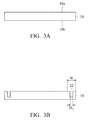
- FIGS. 3A to 3G are cross-sectional diagrams illustrating an exemplary embodiment of a wafer edge pretreatment for handling a thin wafer
- FIGS. 4A to 4G are cross-sectional diagrams illustrating another exemplary embodiment of a wafer edge pretreatment for handling a thin wafer.
- FIGS. 5A to 5E are cross-sectional diagrams illustrating an exemplary embodiment of an edge protection method for handling a thin wafer.
- FIGS. 1A to 1G illustrate an exemplary embodiment of an edge sealing method for handling a thin wafer.
- FIG. 1A is a cross-sectional view of one embodiment of a wafer 10 attached to a carrier 12 through an adhesive layer.
- a wafer 10 is provided with a plurality of semiconductor chips therein.
- the wafer 10 includes a semiconductor substrate such as silicon, gallium arsenide, a rock crystal wafer, sapphire, glass, and the like.
- the wafer 10 has a first surface 10 a and a second surface 10 b opposite to the first surface 10 a .
- integrated circuits including active and passive devices such as transistors, resistors, capacitors and the like, are formed to connect bond pads and/or other interconnection structures.
- the carrier 12 is made of removable or dissolvable material such as glass, metal, ceramics, polymer, silicon, etc.
- the wafer 10 includes a plurality of through silicon vias (TSVs) used for 3D ICs applications.
- TSVs through silicon vias
- a wafer 10 comprises a semiconductor substrate 11 having a front surface 11 a and a back surface 11 b , wherein integrated circuits and interconnect structures are formed on the front surface 11 a , and a plurality of through vias 40 passing through at least a part of the semiconductor substrate 11 .
- the through via 40 is a metal-filled plug extending from the front surface 11 a toward the back surface 11 b and reaching an intended depth.
- the through via 40 can electrically connect a bond pad 42 formed on the interconnect structure.
- first-level interconnection refers to a lowermost metal layer patterned in a lowermost inter-metal dielectric (IMD) layer overlying contact structures and transistors.
- IMD inter-metal dielectric
- the metal-filled via process is performed after the fabrication of interconnect structures.
- FIG. 1B is a cross-sectional view of the wafer 10 undergoing a wafer thinning process.
- the wafer 10 can now be processed in its structure-free area (second surface 10 b ) to the desired final thickness. This can be done, for example, through grinding, etching, and/or polishing, resulting in a thinned wafer 10 ′′ with a predetermined thickness depending on the purpose for which the semiconductor package is used.
- the wafer 10 is thinned to a thickness of from about 5 ⁇ m to about 50 ⁇ m. In another embodiment, the wafer 10 is thinned to a thickness of from about 50 ⁇ m to about 180 ⁇ m.
- one end 40 a of the through via 40 is exposed and/or protruded from the back surface 11 b ′′ of the semiconductor substrate 11 after the wafer thinning process as shown in FIG. 2B .
- FIG. 1C is a cross-sectional view of a plurality of dies 14 bonded onto the thinned wafer 10 ′′, forming a dies-to-wafer stack.
- Backside metallization including electrical connections and/or other structures, are formed on the exposed surface 10 b ′′ of the thinned wafer 10 ′′.
- dies 14 are bonded onto the thinned wafer 10 ′′, wherein the bonding methods include commonly used methods such as oxide-to-oxide bonding, oxide-to-silicon bonding, copper-to-copper bonding, adhesive bonding, and the like.
- the dies 14 may include memory chips, RF (radio frequency) chips, logic chips, or other chips.
- Each of the dies 14 has a first surface 14 a and a second surface 14 b , and integrated circuits are formed on the first surface 14 a .
- the first surface 14 a of the die 14 is bonded on the exposed surface 10 b ′′ of the thinned wafer 10 ′′.
- the second surface 14 b of the die 14 is bonded on the exposed surface 10 b ′′ of the thinned wafer 10 ′′.
- conductive structures 44 such as solder bumps are formed on the exposed ends 40 a of the through vias 40 to bond to the second surface 14 b or the first surface 14 a of the die 14 as shown in FIG. 2C .
- the conductive structures 44 also include redistribution layers and pads which can be formed on the exposed surface 10 b ′′ of the thinned wafer 10 ′′ before forming the solder bumps.
- FIG. 1D is a cross-sectional view of a molding process performed on the dies-to-wafer stack.
- a protection layer 16 such as a molding compound is coated over dies-to-wafer stack and fills the remaining spacing between adjacent dies 14 , but leaves an uncovered region 17 at the edge of the thinned wafer 10 ′′ for supporting in the molding process.
- the uncovered region 17 is a ring of about 2 ⁇ 3 mm at the edge of the thinned wafer 10 ′′.
- the protection layer 16 is formed of a curable material such as, for example a polymer-based material, resin-based material, polyimide, silicon oxide, epoxy, benzocyclobutenes (BCB), SilkTM (Dow Chemical), or a combination thereof.
- the molding process includes injection molding, compression molding, stencil printing, spin-on coating, or future-developed molding processes.
- a curing or baking step is performed to solidify protection material.
- a support structure 18 is formed on the uncovered region 17 at the edge of the thinned wafer 10 ′′ as shown in FIG. 1E .
- the support structure 18 covers at least a portion of the uncovered region 17 to enclose the protection layer 16 .
- the support layer 18 fills the uncovered region 17 to seal the edge of the thinned wafer 10 ′′.
- the support layer 18 can be formed as the same height of the protection layer 16 .
- the support layer 18 is formed of an adhesive material, or a dielectric material such as, for example a polymer-based material, resin-based material, polyimide, epoxy, spin-on glass (SOG), or a combination thereof by using injection, printing, coating, or future-developed depositing processes.
- a tape 20 is laminated on top of the protection layer 16 .
- the tape 20 for example a BG (Backside Grinding) tape, is formed by coating a UV-curing acrylic resin on polyethylene terephthalate (PET) or polyethylene base member, a resist film made of a polyimide resin (photosensitive or anti-photosensitive), or the like is employed.
- FIG. 1G is a cross-sectional diagram showing the dies-to-wafer stack detached from the carrier 12 to expose the first surface 10 a of the thinned wafer 10 ′′.
- the detaching process is performed for example by using a solvent, by using UV irradiation or by being pulled off.
- the use of a solvent or chemical stripper can dissolve the adhesive to allow a disassembly of the wafer-carrier stack.
- external contacts e.g., solder bumps, copper-containing bumps or combinations thereof
- the individual semiconductor chips can be formed on the first surface 10 a of the thinned wafer 10 ′′ for bonding to electrical terminals, where it is then diced in the usual manner along cutting lines to separate the encapsulated dies-to-wafer stack into individual semiconductor packages. After dicing, the stacked chip or chips are mounted on an IC card through, for example, an anisotropically conductive connection film.
- FIG. 3A to FIG. 3G illustrate an exemplary embodiment of a wafer edge pretreatment for handling a thin wafer. Explanation of the same or similar portions to the description in FIG. 1A to FIG. 1G and FIG. 2A to FIG. 2C is omitted herein.
- FIG. 3A is a cross-sectional view of one embodiment of a wafer 10 provided with a plurality of semiconductor chips therein.
- the wafer 10 has a first surface 10 a and a second surface 10 b opposite top the first surface 10 a , and integrated circuits are formed on the first surface 10 a to connect bond pads and/or other interconnection structures.
- a trench 22 is formed at the edge of the wafer 10 as shown in FIG. 3B , followed by filling a dielectric material, resulting in a support structure 24 as shown in FIG. 3C .
- a carrier 12 is then bonded to the adhesive material layer applied on the first surface 10 a for enabling easier handling of the wafer 10 in subsequent thinning process.
- the trench 22 passes through at least a portion of the edge area of the first surface 10 a down to a predetermined depth of the semiconductor substrate.
- the edge area of the wafer 10 has a width W equal to or less than 10 mm defined from the rim of the wafer 10 .
- the width W is about 2-3 mm.
- the trench 22 has a diameter D 1 of more than 0.1 mm.
- the trench 22 has a diameter D 1 of about 1-2 mm formed within the edge area.
- the trench 22 extends to the semiconductor substrate and is, for example, more than 50 mm in depth.
- the trench 22 is a ring-shaped opening adjacent to the rim of the wafer 10 .
- the dielectric material of the support structure 24 is formed of, for example, a polymer-based material, resin-based material, polyimide, epoxy, SOG, or a combination thereof.
- a wafer thinning process is performed on the second surface 10 b of the wafer 10 to reach a desired thickness as shown in FIG. 3D , wherein the support structure 24 ′′ is also thinned down to be exposed.
- a plurality of dies 14 are bonded onto the thinned wafer 10 ′′ and a protection layer 16 is formed on the dies-to-wafer stack in a molding process as depicted in FIG. 3E .
- the uncovered region 17 exposes at least a part of the support structure 24 ′′.
- the protection layer 16 does not cover the support structure 24 ′′.
- the protection layer 16 covers a part of the support structure 24 ′′.
- the above-described wafer edge pretreatment can be applied for handling a wafer 10 including through vias 40 as depicted in FIGS. 2A to 2C .
- FIGS. 4A to 4G illustrate another exemplary embodiment of a wafer edge pretreatment for handling a thin wafer. Explanation of the same or similar portions to the description in FIGS. 3A to 3G is omitted herein.
- a trench 22 ′′ formed at the edge portion of the wafer 10 as shown in FIG. 4B has a diameter D 2 substantially equal to the width W of the edge area of the first surface 10 a .
- the trench 22 ′′ has a diameter D 2 of about 2-3 mm.
- a support structure 24 a is formed at the edge of the wafer 10 .
- the support structure 24 a is also thinned down and exposed, forming a ring at the rim of the exposed surface 10 b ′′ of the thinned wafer 10 ′′ as shown in FIG. 4D .
- the protection layer 16 is coated over the dies-to-wafer stack and fills the remaining spacing between adjacent dies 14 , but leaves an uncovered region 17 at the edge area of the thinned wafer 10 ′′ for supporting in the molding process.
- the uncovered region 17 exposes at least a part of the support structure 24 a ′′.
- the protection layer 16 does not cover the support structure 24 a ′′.
- the protection layer 16 covers a part of the support structure 24 a′′.
- FIGS. 5A to 5E illustrate an exemplary embodiment of an edge protection method for handling a thin wafer. Explanation of the same or similar portions to the description in FIGS. 1A to 1G is omitted herein.
- a housing 30 is provided for supporting the subsequent molding process as shown in FIG. 5D .
- the housing 30 includes a bottom portion 32 from which a peripheral wall portion 34 extends upwardly to define the concave portion 32 a .
- the dies-to-wafer stack is affixed to the housing 30 by attaching the bottom 12 b of the carrier 12 to the bottom portion 32 using gluing or taping.
- the concave portion 32 a has a planar bottom of an area substantially equal to the bottom area of the carrier 12 , thus the rim of the thinned wafer 10 ′′ is affixed to the peripheral wall portion 34 .
- the housing 30 may be a rigid or a flexible member made from copper, aluminum, plastic, rubber, paper, cardboard, etc.
- a molding process is performed on the dies-to-wafer stack supported by the housing 30 as depicted in FIG. 5E , in which a protection layer 16 can cover the edge of the thinned wafer 10 ′′ without leaving an uncovered region because the peripheral wall portion 34 serves as a support structure for handling the thinned wafer in the molding process and the carrier-detaching process as well.
Landscapes
- Engineering & Computer Science (AREA)
- Internal Circuitry In Semiconductor Integrated Circuit Devices (AREA)
- Manufacturing & Machinery (AREA)
- Structures Or Materials For Encapsulating Or Coating Semiconductor Devices Or Solid State Devices (AREA)
- Mechanical Treatment Of Semiconductor (AREA)
- Microelectronics & Electronic Packaging (AREA)
Abstract
Description
Claims (20)
Priority Applications (3)
| Application Number | Priority Date | Filing Date | Title |
|---|---|---|---|
| US12/717,573 US9117828B2 (en) | 2009-03-27 | 2010-03-04 | Method of handling a thin wafer |
| CN2010101431849A CN101847588B (en) | 2009-03-27 | 2010-03-29 | Semiconductor process |
| TW099109332A TWI494979B (en) | 2009-03-27 | 2010-03-29 | Semiconductor process |
Applications Claiming Priority (2)
| Application Number | Priority Date | Filing Date | Title |
|---|---|---|---|
| US16411209P | 2009-03-27 | 2009-03-27 | |
| US12/717,573 US9117828B2 (en) | 2009-03-27 | 2010-03-04 | Method of handling a thin wafer |
Publications (2)
| Publication Number | Publication Date |
|---|---|
| US20100248427A1 US20100248427A1 (en) | 2010-09-30 |
| US9117828B2 true US9117828B2 (en) | 2015-08-25 |
Family
ID=42784771
Family Applications (1)
| Application Number | Title | Priority Date | Filing Date |
|---|---|---|---|
| US12/717,573 Expired - Fee Related US9117828B2 (en) | 2009-03-27 | 2010-03-04 | Method of handling a thin wafer |
Country Status (2)
| Country | Link |
|---|---|
| US (1) | US9117828B2 (en) |
| TW (1) | TWI494979B (en) |
Families Citing this family (15)
| Publication number | Priority date | Publication date | Assignee | Title |
|---|---|---|---|---|
| JP2013030537A (en) * | 2011-07-27 | 2013-02-07 | Elpida Memory Inc | Method of manufacturing semiconductor device |
| FR2980917B1 (en) * | 2011-09-30 | 2013-09-27 | St Microelectronics Crolles 2 | METHOD FOR PRODUCING AN ELECTRICALLY CONDUCTIVE THROUGH BOND |
| US9111946B2 (en) | 2012-12-20 | 2015-08-18 | Invensas Corporation | Method of thinning a wafer to provide a raised peripheral edge |
| US8928120B1 (en) * | 2013-06-28 | 2015-01-06 | Taiwan Semiconductor Manufacturing Company Limited | Wafer edge protection structure |
| US9209046B2 (en) * | 2013-10-02 | 2015-12-08 | Taiwan Semiconductor Manufacturing Company Ltd. | Semiconductor device and manufacturing method thereof |
| KR102259959B1 (en) | 2013-12-05 | 2021-06-04 | 삼성전자주식회사 | Carrier and a method of fabricating a semiconductor device |
| US20150371956A1 (en) * | 2014-06-19 | 2015-12-24 | Globalfoundries Inc. | Crackstops for bulk semiconductor wafers |
| JP6369405B2 (en) * | 2015-07-07 | 2018-08-08 | 信越化学工業株式会社 | Thermosetting resin composition for semiconductor encapsulation |
| US10957672B2 (en) * | 2017-11-13 | 2021-03-23 | Taiwan Semiconductor Manufacturing Company, Ltd. | Package structure and method of manufacturing the same |
| CN111180324B (en) * | 2019-12-27 | 2023-04-28 | 中芯集成电路(宁波)有限公司 | Thinning method of bonded wafer structure and wafer level packaging structure |
| CN111667770B (en) * | 2020-07-15 | 2021-10-08 | 武汉华星光电技术有限公司 | Flexible display device |
| US11908831B2 (en) * | 2020-10-21 | 2024-02-20 | Stmicroelectronics Pte Ltd | Method for manufacturing a wafer level chip scale package (WLCSP) |
| CN114464529B (en) * | 2022-01-10 | 2025-06-17 | 绍兴同芯成集成电路有限公司 | Method for preparing a semiconductor device |
| CN115295505B (en) * | 2022-07-14 | 2026-03-13 | 中国电子科技集团公司第五十五研究所 | A method for improving the breakdown resistance of devices using BCB resin |
| US20240186263A1 (en) * | 2022-12-01 | 2024-06-06 | Intel Corporation | Structure and process for warpage reduction |
Citations (51)
| Publication number | Priority date | Publication date | Assignee | Title |
|---|---|---|---|---|
| US4811082A (en) | 1986-11-12 | 1989-03-07 | International Business Machines Corporation | High performance integrated circuit packaging structure |
| US4990462A (en) | 1989-04-12 | 1991-02-05 | Advanced Micro Devices, Inc. | Method for coplanar integration of semiconductor ic devices |
| US5075253A (en) | 1989-04-12 | 1991-12-24 | Advanced Micro Devices, Inc. | Method of coplanar integration of semiconductor IC devices |
| US5380681A (en) | 1994-03-21 | 1995-01-10 | United Microelectronics Corporation | Three-dimensional multichip package and methods of fabricating |
| US6002177A (en) | 1995-12-27 | 1999-12-14 | International Business Machines Corporation | High density integrated circuit packaging with chip stacking and via interconnections |
| US6153536A (en) * | 1999-03-04 | 2000-11-28 | International Business Machines Corporation | Method for mounting wafer frame at back side grinding (BSG) tool |
| US6229216B1 (en) | 1999-01-11 | 2001-05-08 | Intel Corporation | Silicon interposer and multi-chip-module (MCM) with through substrate vias |
| US6271059B1 (en) | 1999-01-04 | 2001-08-07 | International Business Machines Corporation | Chip interconnection structure using stub terminals |
| US6279815B1 (en) | 1998-06-17 | 2001-08-28 | International Business Machines Corporation | Stacked chip process carrier |
| US6333206B1 (en) * | 1996-12-24 | 2001-12-25 | Nitto Denko Corporation | Process for the production of semiconductor device |
| US6355501B1 (en) | 2000-09-21 | 2002-03-12 | International Business Machines Corporation | Three-dimensional chip stacking assembly |
| US6434016B2 (en) | 1999-06-18 | 2002-08-13 | Intel Corporation | Apparatus for interconnecting multiple devices on a circuit board |
| US6448661B1 (en) | 2001-02-09 | 2002-09-10 | Samsung Electornics Co., Ltd. | Three-dimensional multi-chip package having chip selection pads and manufacturing method thereof |
| US6461895B1 (en) | 1999-01-05 | 2002-10-08 | Intel Corporation | Process for making active interposer for high performance packaging applications |
| US6570248B1 (en) | 1998-08-31 | 2003-05-27 | Micron Technology, Inc. | Structure and method for a high-performance electronic packaging assembly |
| US6600222B1 (en) | 2002-07-17 | 2003-07-29 | Intel Corporation | Stacked microelectronic packages |
| US6607938B2 (en) | 2001-07-19 | 2003-08-19 | Samsung Electronics Co., Ltd. | Wafer level stack chip package and method for manufacturing same |
| US6661085B2 (en) | 2002-02-06 | 2003-12-09 | Intel Corporation | Barrier structure against corrosion and contamination in three-dimensional (3-D) wafer-to-wafer vertical stack |
| US6762076B2 (en) | 2002-02-20 | 2004-07-13 | Intel Corporation | Process of vertically stacking multiple wafers supporting different active integrated circuit (IC) devices |
| US6790748B2 (en) | 2002-12-19 | 2004-09-14 | Intel Corporation | Thinning techniques for wafer-to-wafer vertical stacks |
| US20050064681A1 (en) * | 2003-09-19 | 2005-03-24 | Wood Alan G. | Support structure for thinning semiconductor substrates and thinning methods employing the support structure |
| US6887769B2 (en) | 2002-02-06 | 2005-05-03 | Intel Corporation | Dielectric recess for wafer-to-wafer and die-to-die metal bonding and method of fabricating the same |
| US6908785B2 (en) | 2001-12-06 | 2005-06-21 | Samsung Electronics Co., Ltd. | Multi-chip package (MCP) with a conductive bar and method for manufacturing the same |
| US6908565B2 (en) | 2002-12-24 | 2005-06-21 | Intel Corporation | Etch thinning techniques for wafer-to-wafer vertical stacks |
| US6924551B2 (en) | 2003-05-28 | 2005-08-02 | Intel Corporation | Through silicon via, folded flex microelectronic package |
| US6943067B2 (en) | 2002-01-08 | 2005-09-13 | Advanced Micro Devices, Inc. | Three-dimensional integrated semiconductor devices |
| US6946384B2 (en) | 2003-06-06 | 2005-09-20 | Intel Corporation | Stacked device underfill and a method of fabrication |
| US6975016B2 (en) | 2002-02-06 | 2005-12-13 | Intel Corporation | Wafer bonding using a flexible bladder press and thinned wafers for three-dimensional (3D) wafer-to-wafer vertical stack integration, and application thereof |
| US7087538B2 (en) | 2004-08-16 | 2006-08-08 | Intel Corporation | Method to fill the gap between coupled wafers |
| US20060219351A1 (en) * | 2005-04-02 | 2006-10-05 | Stats Chippac Ltd. | Wafer strength reinforcement system for ultra thin wafer thinning |
| US7151009B2 (en) | 2004-06-18 | 2006-12-19 | Samsung Electronics Co., Ltd. | Method for manufacturing wafer level chip stack package |
| US7157353B2 (en) * | 2002-03-06 | 2007-01-02 | Micron Technology, Inc. | Method for fabricating encapsulated semiconductor components |
| US7215033B2 (en) | 2003-11-19 | 2007-05-08 | Samsung Electronics Co., Ltd. | Wafer level stack structure for system-in-package and method thereof |
| US7276799B2 (en) | 2003-08-26 | 2007-10-02 | Samsung Electronics Co., Ltd. | Chip stack package and manufacturing method thereof |
| US7279795B2 (en) | 2005-12-29 | 2007-10-09 | Intel Corporation | Stacked die semiconductor package |
| US7307005B2 (en) | 2004-06-30 | 2007-12-11 | Intel Corporation | Wafer bonding with highly compliant plate having filler material enclosed hollow core |
| US7317256B2 (en) | 2005-06-01 | 2008-01-08 | Intel Corporation | Electronic packaging including die with through silicon via |
| US7320928B2 (en) | 2003-06-20 | 2008-01-22 | Intel Corporation | Method of forming a stacked device filler |
| US7345350B2 (en) | 2003-09-23 | 2008-03-18 | Micron Technology, Inc. | Process and integration scheme for fabricating conductive components, through-vias and semiconductor components including conductive through-wafer vias |
| US7402442B2 (en) | 2005-12-21 | 2008-07-22 | International Business Machines Corporation | Physically highly secure multi-chip assembly |
| US7402515B2 (en) | 2005-06-28 | 2008-07-22 | Intel Corporation | Method of forming through-silicon vias with stress buffer collars and resulting devices |
| US7410884B2 (en) | 2005-11-21 | 2008-08-12 | Intel Corporation | 3D integrated circuits using thick metal for backside connections and offset bumps |
| US7432592B2 (en) | 2005-10-13 | 2008-10-07 | Intel Corporation | Integrated micro-channels for 3D through silicon architectures |
| US20080268614A1 (en) * | 2007-04-25 | 2008-10-30 | Ku-Feng Yang | Wafer Bonding |
| US20090001598A1 (en) * | 2007-06-27 | 2009-01-01 | Wen-Chih Chiou | Formation of Through Via before Contact Processing |
| US7494845B2 (en) | 2004-06-22 | 2009-02-24 | Samsung Electronics Co., Ltd. | Method of forming a thin wafer stack for a wafer level package |
| US7528494B2 (en) | 2005-11-03 | 2009-05-05 | International Business Machines Corporation | Accessible chip stack and process of manufacturing thereof |
| US7557597B2 (en) | 2005-06-03 | 2009-07-07 | International Business Machines Corporation | Stacked chip security |
| US7576435B2 (en) | 2007-04-27 | 2009-08-18 | Taiwan Semiconductor Manufacturing Company, Ltd. | Low-cost and ultra-fine integrated circuit packaging technique |
| US7834450B2 (en) | 2007-08-20 | 2010-11-16 | Samsung Electronics Co., Ltd. | Semiconductor package having memory devices stacked on logic device |
| US7973407B2 (en) * | 2003-07-02 | 2011-07-05 | Intel Corporation | Three-dimensional stacked substrate arrangements |
-
2010
- 2010-03-04 US US12/717,573 patent/US9117828B2/en not_active Expired - Fee Related
- 2010-03-29 TW TW099109332A patent/TWI494979B/en not_active IP Right Cessation
Patent Citations (59)
| Publication number | Priority date | Publication date | Assignee | Title |
|---|---|---|---|---|
| US4811082A (en) | 1986-11-12 | 1989-03-07 | International Business Machines Corporation | High performance integrated circuit packaging structure |
| US4990462A (en) | 1989-04-12 | 1991-02-05 | Advanced Micro Devices, Inc. | Method for coplanar integration of semiconductor ic devices |
| US5075253A (en) | 1989-04-12 | 1991-12-24 | Advanced Micro Devices, Inc. | Method of coplanar integration of semiconductor IC devices |
| US5380681A (en) | 1994-03-21 | 1995-01-10 | United Microelectronics Corporation | Three-dimensional multichip package and methods of fabricating |
| US5481133A (en) | 1994-03-21 | 1996-01-02 | United Microelectronics Corporation | Three-dimensional multichip package |
| US6002177A (en) | 1995-12-27 | 1999-12-14 | International Business Machines Corporation | High density integrated circuit packaging with chip stacking and via interconnections |
| US6187678B1 (en) | 1995-12-27 | 2001-02-13 | International Business Machines Corporation | High density integrated circuit packaging with chip stacking and via interconnections |
| US6236115B1 (en) | 1995-12-27 | 2001-05-22 | International Business Machines Corporation | High density integrated circuit packaging with chip stacking and via interconnections |
| US6333206B1 (en) * | 1996-12-24 | 2001-12-25 | Nitto Denko Corporation | Process for the production of semiconductor device |
| US6279815B1 (en) | 1998-06-17 | 2001-08-28 | International Business Machines Corporation | Stacked chip process carrier |
| US6570248B1 (en) | 1998-08-31 | 2003-05-27 | Micron Technology, Inc. | Structure and method for a high-performance electronic packaging assembly |
| US6271059B1 (en) | 1999-01-04 | 2001-08-07 | International Business Machines Corporation | Chip interconnection structure using stub terminals |
| US6461895B1 (en) | 1999-01-05 | 2002-10-08 | Intel Corporation | Process for making active interposer for high performance packaging applications |
| US6229216B1 (en) | 1999-01-11 | 2001-05-08 | Intel Corporation | Silicon interposer and multi-chip-module (MCM) with through substrate vias |
| US6562653B1 (en) | 1999-01-11 | 2003-05-13 | Intel Corporation | Silicon interposer and multi-chip-module (MCM) with through substrate vias |
| US6153536A (en) * | 1999-03-04 | 2000-11-28 | International Business Machines Corporation | Method for mounting wafer frame at back side grinding (BSG) tool |
| US6434016B2 (en) | 1999-06-18 | 2002-08-13 | Intel Corporation | Apparatus for interconnecting multiple devices on a circuit board |
| US6355501B1 (en) | 2000-09-21 | 2002-03-12 | International Business Machines Corporation | Three-dimensional chip stacking assembly |
| US6448661B1 (en) | 2001-02-09 | 2002-09-10 | Samsung Electornics Co., Ltd. | Three-dimensional multi-chip package having chip selection pads and manufacturing method thereof |
| US6607938B2 (en) | 2001-07-19 | 2003-08-19 | Samsung Electronics Co., Ltd. | Wafer level stack chip package and method for manufacturing same |
| US7531890B2 (en) | 2001-12-06 | 2009-05-12 | Samsung Electronics Co., Ltd. | Multi-chip package (MCP) with a conductive bar and method for manufacturing the same |
| US6908785B2 (en) | 2001-12-06 | 2005-06-21 | Samsung Electronics Co., Ltd. | Multi-chip package (MCP) with a conductive bar and method for manufacturing the same |
| US6943067B2 (en) | 2002-01-08 | 2005-09-13 | Advanced Micro Devices, Inc. | Three-dimensional integrated semiconductor devices |
| US7056807B2 (en) | 2002-02-06 | 2006-06-06 | Intel Corporation | Barrier structure against corrosion and contamination in three-dimensional (3-D) wafer-to-wafer vertical stack |
| US6887769B2 (en) | 2002-02-06 | 2005-05-03 | Intel Corporation | Dielectric recess for wafer-to-wafer and die-to-die metal bonding and method of fabricating the same |
| US6661085B2 (en) | 2002-02-06 | 2003-12-09 | Intel Corporation | Barrier structure against corrosion and contamination in three-dimensional (3-D) wafer-to-wafer vertical stack |
| US6975016B2 (en) | 2002-02-06 | 2005-12-13 | Intel Corporation | Wafer bonding using a flexible bladder press and thinned wafers for three-dimensional (3D) wafer-to-wafer vertical stack integration, and application thereof |
| US7037804B2 (en) | 2002-02-06 | 2006-05-02 | Intel Corporation | Wafer bonding using a flexible bladder press for three dimensional (3D) vertical stack integration |
| US6762076B2 (en) | 2002-02-20 | 2004-07-13 | Intel Corporation | Process of vertically stacking multiple wafers supporting different active integrated circuit (IC) devices |
| US7157787B2 (en) | 2002-02-20 | 2007-01-02 | Intel Corporation | Process of vertically stacking multiple wafers supporting different active integrated circuit (IC) devices |
| US7157353B2 (en) * | 2002-03-06 | 2007-01-02 | Micron Technology, Inc. | Method for fabricating encapsulated semiconductor components |
| US6600222B1 (en) | 2002-07-17 | 2003-07-29 | Intel Corporation | Stacked microelectronic packages |
| US6790748B2 (en) | 2002-12-19 | 2004-09-14 | Intel Corporation | Thinning techniques for wafer-to-wafer vertical stacks |
| US6908565B2 (en) | 2002-12-24 | 2005-06-21 | Intel Corporation | Etch thinning techniques for wafer-to-wafer vertical stacks |
| US6924551B2 (en) | 2003-05-28 | 2005-08-02 | Intel Corporation | Through silicon via, folded flex microelectronic package |
| US6946384B2 (en) | 2003-06-06 | 2005-09-20 | Intel Corporation | Stacked device underfill and a method of fabrication |
| US7320928B2 (en) | 2003-06-20 | 2008-01-22 | Intel Corporation | Method of forming a stacked device filler |
| US7973407B2 (en) * | 2003-07-02 | 2011-07-05 | Intel Corporation | Three-dimensional stacked substrate arrangements |
| US7276799B2 (en) | 2003-08-26 | 2007-10-02 | Samsung Electronics Co., Ltd. | Chip stack package and manufacturing method thereof |
| US20050064681A1 (en) * | 2003-09-19 | 2005-03-24 | Wood Alan G. | Support structure for thinning semiconductor substrates and thinning methods employing the support structure |
| US7345350B2 (en) | 2003-09-23 | 2008-03-18 | Micron Technology, Inc. | Process and integration scheme for fabricating conductive components, through-vias and semiconductor components including conductive through-wafer vias |
| US7215033B2 (en) | 2003-11-19 | 2007-05-08 | Samsung Electronics Co., Ltd. | Wafer level stack structure for system-in-package and method thereof |
| US7151009B2 (en) | 2004-06-18 | 2006-12-19 | Samsung Electronics Co., Ltd. | Method for manufacturing wafer level chip stack package |
| US7494845B2 (en) | 2004-06-22 | 2009-02-24 | Samsung Electronics Co., Ltd. | Method of forming a thin wafer stack for a wafer level package |
| US7307005B2 (en) | 2004-06-30 | 2007-12-11 | Intel Corporation | Wafer bonding with highly compliant plate having filler material enclosed hollow core |
| US7087538B2 (en) | 2004-08-16 | 2006-08-08 | Intel Corporation | Method to fill the gap between coupled wafers |
| US20060219351A1 (en) * | 2005-04-02 | 2006-10-05 | Stats Chippac Ltd. | Wafer strength reinforcement system for ultra thin wafer thinning |
| US7317256B2 (en) | 2005-06-01 | 2008-01-08 | Intel Corporation | Electronic packaging including die with through silicon via |
| US7557597B2 (en) | 2005-06-03 | 2009-07-07 | International Business Machines Corporation | Stacked chip security |
| US7402515B2 (en) | 2005-06-28 | 2008-07-22 | Intel Corporation | Method of forming through-silicon vias with stress buffer collars and resulting devices |
| US7432592B2 (en) | 2005-10-13 | 2008-10-07 | Intel Corporation | Integrated micro-channels for 3D through silicon architectures |
| US7528494B2 (en) | 2005-11-03 | 2009-05-05 | International Business Machines Corporation | Accessible chip stack and process of manufacturing thereof |
| US7410884B2 (en) | 2005-11-21 | 2008-08-12 | Intel Corporation | 3D integrated circuits using thick metal for backside connections and offset bumps |
| US7402442B2 (en) | 2005-12-21 | 2008-07-22 | International Business Machines Corporation | Physically highly secure multi-chip assembly |
| US7279795B2 (en) | 2005-12-29 | 2007-10-09 | Intel Corporation | Stacked die semiconductor package |
| US20080268614A1 (en) * | 2007-04-25 | 2008-10-30 | Ku-Feng Yang | Wafer Bonding |
| US7576435B2 (en) | 2007-04-27 | 2009-08-18 | Taiwan Semiconductor Manufacturing Company, Ltd. | Low-cost and ultra-fine integrated circuit packaging technique |
| US20090001598A1 (en) * | 2007-06-27 | 2009-01-01 | Wen-Chih Chiou | Formation of Through Via before Contact Processing |
| US7834450B2 (en) | 2007-08-20 | 2010-11-16 | Samsung Electronics Co., Ltd. | Semiconductor package having memory devices stacked on logic device |
Also Published As
| Publication number | Publication date |
|---|---|
| TWI494979B (en) | 2015-08-01 |
| US20100248427A1 (en) | 2010-09-30 |
| TW201036055A (en) | 2010-10-01 |
Similar Documents
| Publication | Publication Date | Title |
|---|---|---|
| US9117828B2 (en) | Method of handling a thin wafer | |
| US8252665B2 (en) | Protection layer for adhesive material at wafer edge | |
| US7883991B1 (en) | Temporary carrier bonding and detaching processes | |
| US10636773B2 (en) | Semiconductor package structure and method for forming the same | |
| CN107026092B (en) | Method of manufacturing fingerprint scanner and semiconductor device | |
| TWI556349B (en) | Structure of semiconductor device and method of manufacturing the same | |
| US10269619B2 (en) | Wafer level chip scale packaging intermediate structure apparatus and method | |
| US20190131243A1 (en) | Integrated fan-out package and method of fabricating the same | |
| CN101740415B (en) | Integrated circuit structure and method of forming the same | |
| KR101157726B1 (en) | Ultra-thin stacked chips packaging | |
| US20240371776A1 (en) | Manufacturing method of semiconductor package | |
| US11776838B2 (en) | Semiconductor package and manufacturing method thereof | |
| US11996400B2 (en) | Manufacturing method of package on package structure | |
| CN111033732A (en) | Stackable memory die using hybrid addition structure of wire bonds | |
| TWI767287B (en) | A semiconductor package structure | |
| CN109427700A (en) | Integrated circuit package and method of making the same | |
| CN104051399B (en) | Crystal wafer chip dimension encapsulation intermediate structure device and method | |
| US11244879B2 (en) | Semiconductor package | |
| CN115799087A (en) | Package, package-on-package structure and method of manufacturing package-on-package structure | |
| US10991597B2 (en) | Method of fabricating a semiconductor device using an adhesive layer | |
| CN101847588B (en) | Semiconductor process |
Legal Events
| Date | Code | Title | Description |
|---|---|---|---|
| AS | Assignment |
Owner name: TAIWAN SEMICONDUCTOR MANUFACTURING COMPANY, LTD., Free format text: ASSIGNMENT OF ASSIGNORS INTEREST;ASSIGNORS:WU, WENG-JIN;YANG, KU-FENG;CHIOU, WEN-CHIH;REEL/FRAME:024030/0094 Effective date: 20100225 |
|
| ZAAA | Notice of allowance and fees due |
Free format text: ORIGINAL CODE: NOA |
|
| ZAAB | Notice of allowance mailed |
Free format text: ORIGINAL CODE: MN/=. |
|
| STCF | Information on status: patent grant |
Free format text: PATENTED CASE |
|
| MAFP | Maintenance fee payment |
Free format text: PAYMENT OF MAINTENANCE FEE, 4TH YEAR, LARGE ENTITY (ORIGINAL EVENT CODE: M1551); ENTITY STATUS OF PATENT OWNER: LARGE ENTITY Year of fee payment: 4 |
|
| FEPP | Fee payment procedure |
Free format text: MAINTENANCE FEE REMINDER MAILED (ORIGINAL EVENT CODE: REM.); ENTITY STATUS OF PATENT OWNER: LARGE ENTITY |
|
| LAPS | Lapse for failure to pay maintenance fees |
Free format text: PATENT EXPIRED FOR FAILURE TO PAY MAINTENANCE FEES (ORIGINAL EVENT CODE: EXP.); ENTITY STATUS OF PATENT OWNER: LARGE ENTITY |
|
| STCH | Information on status: patent discontinuation |
Free format text: PATENT EXPIRED DUE TO NONPAYMENT OF MAINTENANCE FEES UNDER 37 CFR 1.362 |
|
| FP | Lapsed due to failure to pay maintenance fee |
Effective date: 20230825 |