US9112276B2 - Wideband antenna with low passive intermodulation attributes - Google Patents
Wideband antenna with low passive intermodulation attributes Download PDFInfo
- Publication number
- US9112276B2 US9112276B2 US13/848,618 US201313848618A US9112276B2 US 9112276 B2 US9112276 B2 US 9112276B2 US 201313848618 A US201313848618 A US 201313848618A US 9112276 B2 US9112276 B2 US 9112276B2
- Authority
- US
- United States
- Prior art keywords
- antenna
- radiator
- antenna radiator
- antenna assembly
- ground plane
- Prior art date
- Legal status (The legal status is an assumption and is not a legal conclusion. Google has not performed a legal analysis and makes no representation as to the accuracy of the status listed.)
- Expired - Fee Related, expires
Links
Images


Classifications
-
- H—ELECTRICITY
- H01—ELECTRIC ELEMENTS
- H01Q—ANTENNAS, i.e. RADIO AERIALS
- H01Q1/00—Details of, or arrangements associated with, antennas
- H01Q1/42—Housings not intimately mechanically associated with radiating elements, e.g. radome
-
- H—ELECTRICITY
- H01—ELECTRIC ELEMENTS
- H01Q—ANTENNAS, i.e. RADIO AERIALS
- H01Q1/00—Details of, or arrangements associated with, antennas
- H01Q1/12—Supports; Mounting means
- H01Q1/1207—Supports; Mounting means for fastening a rigid aerial element
-
- H—ELECTRICITY
- H01—ELECTRIC ELEMENTS
- H01Q—ANTENNAS, i.e. RADIO AERIALS
- H01Q5/00—Arrangements for simultaneous operation of antennas on two or more different wavebands, e.g. dual-band or multi-band arrangements
- H01Q5/30—Arrangements for providing operation on different wavebands
- H01Q5/307—Individual or coupled radiating elements, each element being fed in an unspecified way
- H01Q5/342—Individual or coupled radiating elements, each element being fed in an unspecified way for different propagation modes
- H01Q5/357—Individual or coupled radiating elements, each element being fed in an unspecified way for different propagation modes using a single feed point
- H01Q5/364—Creating multiple current paths
- H01Q5/371—Branching current paths
-
- H—ELECTRICITY
- H01—ELECTRIC ELEMENTS
- H01Q—ANTENNAS, i.e. RADIO AERIALS
- H01Q9/00—Electrically-short antennas having dimensions not more than twice the operating wavelength and consisting of conductive active radiating elements
- H01Q9/04—Resonant antennas
-
- H—ELECTRICITY
- H01—ELECTRIC ELEMENTS
- H01Q—ANTENNAS, i.e. RADIO AERIALS
- H01Q9/00—Electrically-short antennas having dimensions not more than twice the operating wavelength and consisting of conductive active radiating elements
- H01Q9/04—Resonant antennas
- H01Q9/30—Resonant antennas with feed to end of elongated active element, e.g. unipole
- H01Q9/32—Vertical arrangement of element
- H01Q9/36—Vertical arrangement of element with top loading
-
- Y—GENERAL TAGGING OF NEW TECHNOLOGICAL DEVELOPMENTS; GENERAL TAGGING OF CROSS-SECTIONAL TECHNOLOGIES SPANNING OVER SEVERAL SECTIONS OF THE IPC; TECHNICAL SUBJECTS COVERED BY FORMER USPC CROSS-REFERENCE ART COLLECTIONS [XRACs] AND DIGESTS
- Y10—TECHNICAL SUBJECTS COVERED BY FORMER USPC
- Y10T—TECHNICAL SUBJECTS COVERED BY FORMER US CLASSIFICATION
- Y10T29/00—Metal working
- Y10T29/49—Method of mechanical manufacture
- Y10T29/49002—Electrical device making
- Y10T29/49016—Antenna or wave energy "plumbing" making
Definitions
- This invention relates generally to the field of wireless communication.
- the present invention relates to a wideband antenna having low passive intermodulation attributes for use within a distributed antenna system, the antenna being configured for robust multi-band operation for use in wireless communications.
- a distributed antenna system is a network of spatially separated antenna nodes connected to a common source via a transport medium that provides wireless service within a geographic area or structure.
- the idea is to split the transmitted power among several antenna elements, separated in space so as to provide coverage over the same area as a single antenna but with reduced total power and improved reliability.
- a single antenna radiating at high power is replaced by a group of low-power antennas to cover the same area.
- PIM Passive Intermodulation
- a wideband antenna for use in distributed antenna systems is described, the antenna being capable of efficient transmission and reception in multiple frequency bands while maintaining low passive intermodulation (PIM) performance.
- PIM passive intermodulation
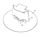
- FIG. 1 illustrates a top perspective view of the antenna housing according to an embodiment of the invention.
- FIG. 2 illustrates a bottom perspective view of the antenna of FIG. 1 .
- FIG. 3 illustrates a mounting bracket adapted for mounting the antenna housing of FIG. 1 to a flat surface.
- FIG. 4 illustrates a cross section of an antenna and housing in accordance with FIGS. 1-3 .
- FIG. 5 illustrates a base plate for receiving an antenna element in accordance with certain embodiments; the base plate forms a ground plane.
- FIG. 6 illustrates a wideband antenna received within a portion of the base plate of FIG. 5 .
- FIG. 7 illustrates a wideband antenna according to various embodiments.
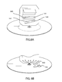
- FIGS. 8 illustrate an antenna having configurable flap portions, and an RF current flow induced on the ground plane, respectively.
- FIGS. 9(A-B) illustrate a side view, and top view, of an antenna having configurable flap portions arranged at acute angles with respect to the antenna radiator, respectively.
- FIGS. 10(A-B) illustrate a side view, and top view, of an antenna having configurable flap portions arranged at right angles with respect to the antenna radiator, respectively.
- FIGS. 11(A-B) illustrate a side view, and top view, of an antenna having configurable flap portions arranged at obtuse angles with respect to the antenna radiator, respectively.
- FIG. 12 illustrates an antenna with configurable flaps shaped to alter the antenna near field, and an associated RF current flowing about the antenna radiator.
- FIG. 13 illustrates an antenna according to various embodiments, the antenna comprising a parasitic conductor element positioned adjacent to the antenna radiator and supported by non-conductive vertical supports extending upwardly from the base plate.
- FIG. 14 illustrates an antenna with a parasitic conductor element configured to extend through a vertical plane of the antenna radiator.
- FIGS. 15-16 illustrate the antenna according to various embodiments of the invention and one or more apertures disposed on the antenna base plate; the antenna radiator creating a coupled RF current with the base plate and the apertures creating a reflected RF current.
- FIG. 17 illustrates dielectric volumes disposed about one or more apertures of the base plate.
- FIGS. 18-19 illustrate the antenna according to various embodiments and further comprising an active4 tuning element connecting the parasitic conductor element to the base plate for providing an ability to alter the antenna radiation pattern.
- FIGS. 20-21 illustrate the antenna according to various embodiments and further comprising one or more coupled plates disposed within the antenna housing and positioned proximal and parallel to the horizontal top portion of the antenna radiator.
- FIGS. 22-23 illustrate the antenna according to various embodiments and further comprising one or more connected plates disposed within the antenna housing and positioned proximal and parallel to the horizontal top portion of the antenna radiator.
- FIG. 24 is a schematic representing a low PIM antenna design methodology.
- the invention provides a wideband antenna for use in distributed antenna systems, the antenna being capable of efficient transmission and reception in multiple frequency bands while maintaining low passive intermodulation (PIM) performance.
- PIM passive intermodulation
- a first conductor element is vertically disposed within an antenna housing, the first conductor element originates from a planar stock and is cut and bent to form a planar body portion and a planar top portion aligned substantially perpendicular to the planar body portion.
- the first conductor element further comprises one or more configurable flap portions cut out from the planar body portion and adapted to be bent into a configured position at an angle with respect to the planar body portion.
- a second planar conductor element is horizontally disposed within the antenna housing and comprises a non-conductive bracket attached at a hole disposed at or near a center thereof. The first conductor is attached to the second conductor at the non-conductive support bracket, thus forming an antenna radiator positioned above a ground plane.
- the first conductor further comprises a transmission line conductor extending therefrom through the hole of the second conductor.
- a coaxial cable is connected such that the second conductor is connected to ground and the transmission line conductor is connected to the antenna feed.
- a third conductor or “parasitic conductor element” is positioned adjacent to the first conductor or “antenna radiator”.
- the third conductor is dimensioned to resonate at a frequency to provide increased bandwidth at one or multiple resonances of the antenna formed by the first and second conductors.
- one or more apertures are disposed on the base plate or “ground plane”.
- the apertures comprise dimensions designed to alter the Passive Intermodulation (PIM) characteristics of the antenna formed by the combination of the first and second conductors.
- PIM Passive Intermodulation
- one or more dielectric volumes of material can be disposed at or near the apertures of the base plate.
- the dielectric material provides a mechanism for altering the PIM characteristics of the antenna.
- one or more coupled or connected plates may be positioned adjacent to the horizontal top portion of the first conductor.
- an active tuning element is provided.
- the active tuning element may be used to connect the third conductor to the base plate.
- An additional signal may be provided to control the active tuning element.
- impedance or phase of the third conductor can be actively adjusted.
- the active tuning element may comprise any tunable capacitor, switch, varactor diode, PIN diode, or other component that can be used to alter impedance of phase delay. By adjusting the impedance and/or phase of the third conductor, the frequency response of the antenna can be adjusted.
- the antenna can be configured to cover multiple cellular frequency bands to provide a single antenna solution for use with multiple transceivers.
- a single-conductor antenna radiator design along with features integrated into the antenna ground plane result in low PIM characteristics during high power transmission.
- One or multiple parasitic elements can be coupled to the driven antenna radiator to enhance bandwidth while still maintaining low PIM characteristics.
- FIG. 1 illustrates a top perspective view of the antenna assembly 100 and outer housing 101 thereof in accordance with various embodiments of the invention.
- the housing is generally a non-conductive plastic structure.
- the antenna and housing are collectively referred to herein as the “antenna assembly 100 ”.
- FIG. 2 further illustrates the antenna and housing of FIG. 1 with a bottom perspective view thereof.
- a coaxial connector 103 is disposed at the bottom side of the base plate 102 at or near a center thereof.
- FIG. 3 illustrates a mounting bracket 110 for use in mounting the antenna assembly with a ceiling or wall.
- One or more clips 111 may extend from the mounting bracket and can be formed of a dielectric material. The clips can be adapted to engage a portion of the base plate of the antenna assembly.
- FIG. 4 illustrates a cross section of the antenna assembly 100 in accordance with a preferred embodiment.
- the antenna assembly comprises a first conductor 120 or “antenna radiator” being vertically disposed above a horizontal second conductor 102 or “base plate/ground plane”.
- the first conductor 120 is structurally supported above the second conductor 102 by a non-conductive support bracket 130 .
- the first conductor is further connected to a transmission line conductor extending through a hole near a center of the second conductor and coupled to a feed portion of the coaxial connector 103 .
- One or more non-conductive clips 111 may extend from the mounting bracket 110 .
- the antenna housing 101 surrounds and protects the antenna components.
- FIG. 5 further illustrates a top perspective view of the base plate 102 having a hole disposed near a center thereof and a non-conductive support bracket 130 attached at the hole.
- the transmission line conductor 104 extends through the hole of the second conductor and a hole of the support bracket 130 such that the first conductor can be connected therewith.
- FIG. 6 illustrates a top perspective view of the antenna in accordance with embodiments illustrated in the previous figures.
- the first conductor 120 or “antenna radiator” is disposed at the non-conductive support bracket 130 and extends upwardly therefrom.
- the antenna radiator is vertically disposed above the base plate 102 .
- FIG. 7 illustrates the first conductor 120 in accordance with various embodiments of the invention.
- the first conductor comprises a vertically disposed body portion 123 extending from a bottom end 124 to a top end.
- the first conductor is cut to allow a top portion thereof to be bent at one or more edges 125 and configured such that the top portion forms a T-shape when viewed from a side thereof.
- the first conductor 120 comprises a horizontally disposed top portion 121 being substantially perpendicularly disposed with respect to a vertically disposed planar body portion 123 . With a portion being cut and bent to form the planar top portion 121 , a hole 122 resides between the top portion 121 and the body portion.
- a monolithic conductive plate can be etched or cut in a u-shape, and the top portion folded along two resulting edges such that a top portion forms a t-shape structure with the body portion when viewed from a side thereof.
- FIG. 8 illustrates an antenna as described in the previous figures and further comprising one or more configurable flap portions etched or cut from the body portion of the antenna radiator.
- the configurable flap portions can be bent or shaped to provide adjustment of the RF current induced on the antenna radiator such that PIM characteristics of the antenna can be improved.
- FIG. 8B illustrates radiofrequency (RF) currents being induced on the antenna radiator, and the coupling between the antenna radiator and the base plate.
- An aperture 150 is disposed on the base plate of the antenna for canceling, absorbing, or reflecting the RF currents 160 for improving the PIM attributes of the antenna assembly.
- the size and or shape of the aperture 150 can be tailored to alter the PIM attributes of the antenna.
- the antenna radiator is positioned above the ground plane.
- the top portion of the antenna radiator is bent in a fashion to provide top loading of the antenna radiator.
- a section of the body portion is cut to allow for formation of a three-dimensional element from a two dimensional element.
- Two configurable flap portions of the antenna body are formed into a three-dimensional shape.
- the transmission line conductor is attached to antenna radiator and is used to transmit and receive signals to and/or from the antenna.
- RF current flow on the antenna radiator is shown, along with coupling of the electric field to the ground plane.
- RF current flow induced on the ground plane and reflected from an aperture in the ground plane is shown.
- FIGS. 9-11 illustrate a number of configurations that may be provided using the configurable flap portions of the antenna radiator.
- the configurable flap portions 140 are individually bent to form acute angles with respect to the planar body portion of the antenna radiator 120 .
- the configurable flap portions 140 are individually bent to form right angles with respect to the planar body portion of the antenna radiator 120 .
- the configurable flap portions 140 are individually bent to form obtuse angles with respect to the planar body portion of the antenna radiator 120 .
- FIGS. 9(A-B) the configurable flap portions 140 are individually bent to form obtuse angles with respect to the planar body portion of the antenna radiator 120 .
- FIG. 12 further illustrates the antenna of FIGS. 8-11 , wherein RF currents 160 are distributed about the antenna radiator 120 and base plate 102 . Additionally, a dielectric volume 151 is positioned at an aperture and provided for adjusting the PIM attributes of the antenna, RF currents 160 are reflected from the aperture and dielectric volume of material 151 thereon.
- FIG. 13 illustrates the antenna further comprising a third conductor referred to herein as a “parasitic conductor element 170 ” positioned adjacent to the antenna radiator 120 and supported by non-conductive vertical supports 171 .
- a third conductor referred to herein as a “parasitic conductor element 170 ” positioned adjacent to the antenna radiator 120 and supported by non-conductive vertical supports 171 .
- the parasitic conductive element may be positioned aside the antenna radiator 120 or may be aligned to extend perpendicular with or through the hole 122 of the antenna radiator 120 as illustrated in FIG. 14 .
- the parasitic conductor element 170 can be dimensioned to resonate at a frequency to provide increased bandwidth at one or multiple resonances formed by the antenna radiator and base plate. Although only one parasitic conductor element is being illustrated, it should be understood that two or more parasitic elements may be incorporated in a similar fashion.
- FIG. 15 illustrates an example of multiple apertures, such as circular holes 150 A and 150 B, cut into the ground plane 102 .
- RF current 160 on antenna radiator 120 couples to the ground plane 102 and portions of the RF current are reflected from the apertures 150 A and 150 B, respectively.
- FIG. 16 illustrates an example of multiple apertures, such independent shapes 152 and 153 , cut into the ground plane 102 .
- RF current 160 on antenna radiator 120 couples to the ground plane 102 and portions of the RF current are reflected from the apertures 152 , and 153 , respectively.
- FIG. 17 illustrates an example of dielectric volumes 151 A, 151 B, and 151 C inserted into apertures cut into ground plane 102 .
- Antenna radiator 120 is attached to the transmission line conductor 104 of an RF connector.
- the dielectric volumes are adapted to alter the electrical characteristics of the apertures.
- the dielectric volumes may comprise distinct dielectric constants, for example where two dielectric volumes and two apertures are provided a first dielectric volume may comprise a first dielectric constant and a second dielectric volume may comprise a second dielectric constant.
- FIG. 18 illustrates an example of an active component 180 coupled to a parasitic conductor element 170 which is positioned in proximity to antenna radiator 120 , which is in turn positioned above a ground plane 102 .
- Non-conductive supports 171 are used to support the parasitic element.
- the active component is used to alter the impedance of the parasitic element which in turn will alter the frequency response of the antenna radiator 120 .
- FIG. 19 illustrates an example of an active component 64 coupled to a parasitic conductor element 170 which is positioned in proximity to antenna radiator 120 , which is in turn positioned above a ground plane 102 .
- Non-conductive support 171 is used to support the parasitic element.
- the parasitic element passes through a hole 122 formed in body portion of the antenna radiator 120 .
- the active component is used to alter the impedance of the parasitic element which in turn will alter the frequency response of the antenna radiator 120 .
- FIG. 20 illustrates an example of a coupled plate conductor 190 positioned in proximity to the horizontal top portion of the antenna radiator 120 .
- Antenna radiator 120 is positioned in proximity to ground plane 102 , and antenna radiator 120 is attached to the transmission line conductor of an RF connector.
- the coupled plate conductor may be embedded or attached to the non conductive housing and arranged thereabout to align adjacent to the antenna radiator when the housing antenna assembly is completely assembled.
- the coupled plate conductor 190 is adapted to electrically couple with the horizontal top portion of the antenna radiator 120 for changing the radiating characteristics of the antenna.
- FIG. 21 illustrates an example of multiple coupled plate conductors 190 A, 190 B, and 190 C positioned in proximity to antenna radiator 120 .
- Antenna radiator 120 is positioned in proximity to ground plane 120 , and antenna radiator 120 is attached to the transmission line conductor of an RF connector.
- multiple coupling plates are adapted to couple with the antenna radiator for altering radiation characteristics of the antenna.
- the multiple coupled plate conductors are each individually embedded or attached to the housing 101 using a non-conductive attachment arm 191 A, 191 B, and 191 C.
- FIG. 22 illustrates an example of a connected conductor assembly 195 positioned in proximity to antenna radiator 120 .
- Connected conductor assembly 195 comprises multiple individual conductor plates ( 196 A-C) which are electrically connected to one another.
- Antenna radiator 120 is positioned in proximity to ground plane 102 , and antenna radiator 120 is attached to the transmission line conductor of an RF connector. Because the connected conductors are electrically connected, the changes induced on the antenna radiator are distinct from changes of similarly oriented non-connected conductor plates. As above, the plates can be embedded within or attached to the housing 101 .
- FIG. 23 illustrates an example of attached conductor plates 199 A and 199 B positioned in proximity to antenna radiator 120 .
- Antenna radiator 120 is positioned in proximity to ground plane 102 , and antenna radiator 120 is attached to the transmission line conductor of an RF connector. This embodiment is distinct in that the conductor plates are attached to the antenna radiator at the horizontal top portion.
- FIG. 24 illustrates a design methodology for a low PIM antenna.
- the methodology includes antenna radiator design, base plate design, antenna radiator and base plate optimization, and testing for PIM requirements.
- Antenna radiator design includes consideration of return loss, efficiency, radiation patterns, and PIM.
- Base plate design includes consideration of PIM, radiation patterns, and return loss.
- Antenna radiator and base plate optimization includes consideration of return loss, PIM, efficiency, and radiation patterns.
Abstract
Description
Claims (17)
Priority Applications (1)
| Application Number | Priority Date | Filing Date | Title |
|---|---|---|---|
| US13/848,618 US9112276B2 (en) | 2012-03-21 | 2013-03-21 | Wideband antenna with low passive intermodulation attributes |
Applications Claiming Priority (2)
| Application Number | Priority Date | Filing Date | Title |
|---|---|---|---|
| US201261613492P | 2012-03-21 | 2012-03-21 | |
| US13/848,618 US9112276B2 (en) | 2012-03-21 | 2013-03-21 | Wideband antenna with low passive intermodulation attributes |
Publications (2)
| Publication Number | Publication Date |
|---|---|
| US20130285877A1 US20130285877A1 (en) | 2013-10-31 |
| US9112276B2 true US9112276B2 (en) | 2015-08-18 |
Family
ID=49476768
Family Applications (1)
| Application Number | Title | Priority Date | Filing Date |
|---|---|---|---|
| US13/848,618 Expired - Fee Related US9112276B2 (en) | 2012-03-21 | 2013-03-21 | Wideband antenna with low passive intermodulation attributes |
Country Status (1)
| Country | Link |
|---|---|
| US (1) | US9112276B2 (en) |
Cited By (5)
| Publication number | Priority date | Publication date | Assignee | Title |
|---|---|---|---|---|
| USD843862S1 (en) * | 2017-07-26 | 2019-03-26 | Symbol Technologies, Llc | Asset tracking equipment housing |
| CN110994127A (en) * | 2019-12-27 | 2020-04-10 | 浙江海通通讯电子股份有限公司 | Ultra-wideband terminal product external antenna |
| USD899278S1 (en) * | 2019-03-05 | 2020-10-20 | Zebra Technologies Corporation | Asset tracking equipment housing |
| US11139576B2 (en) * | 2019-04-03 | 2021-10-05 | Chung Ang University Industry Academic Cooperation Foundation | Planar multipole antenna |
| USD966127S1 (en) | 2020-01-08 | 2022-10-11 | Zebra Technologies Corporation | Asset tracking equipment housing |
Families Citing this family (10)
| Publication number | Priority date | Publication date | Assignee | Title |
|---|---|---|---|---|
| GB2508383B (en) * | 2012-11-29 | 2014-12-17 | Aceaxis Ltd | Processing interference due to non-linear products in a wireless network |
| US10312583B2 (en) * | 2013-09-17 | 2019-06-04 | Laird Technologies, Inc. | Antenna systems with low passive intermodulation (PIM) |
| JP5937147B2 (en) * | 2014-06-26 | 2016-06-22 | 原田工業株式会社 | Antenna unit |
| DE102015202801A1 (en) * | 2015-02-17 | 2016-08-18 | Robert Bosch Gmbh | Antenna arrangement and method for producing an antenna arrangement |
| US10756435B2 (en) * | 2016-04-18 | 2020-08-25 | Ethertronics, Inc. | Low profile antenna module |
| US10263341B2 (en) | 2016-04-19 | 2019-04-16 | Ethertronics, Inc. | Low profile antenna system |
| US11069959B1 (en) * | 2016-05-06 | 2021-07-20 | Commscope Technologies Llc | Monolithic radiating elements and feedboard assemblies for base station antennas formed via laser direct structuring and other selective metallization techniques |
| CN106654537A (en) * | 2017-01-10 | 2017-05-10 | 江苏省东方世纪网络信息有限公司 | Antenna |
| CN209249673U (en) * | 2019-02-02 | 2019-08-13 | 康普技术有限责任公司 | Antenna for base station |
| CN110011037B (en) * | 2019-04-12 | 2024-01-30 | 深圳市安拓浦科技有限公司 | Vertical polarization omnidirectional antenna and dual-polarization omnidirectional antenna thereof |
Citations (4)
| Publication number | Priority date | Publication date | Assignee | Title |
|---|---|---|---|---|
| US6121935A (en) * | 1996-07-02 | 2000-09-19 | Omnipoint Corporation | Folded mono-bow antennas and antenna systems for use in cellular and other wireless communications systems |
| US20040263400A1 (en) * | 2003-06-26 | 2004-12-30 | Alps Electric Co., Ltd. | Antenna system with high gain for radio waves polarized in particular direction |
| US20050140554A1 (en) * | 2003-12-24 | 2005-06-30 | Nokia Corporation | Antenna for mobile communication terminals |
| US20090224991A1 (en) * | 2008-03-05 | 2009-09-10 | Ethertronics, Inc. | Antenna and method for steering antenna beam direction |
-
2013
- 2013-03-21 US US13/848,618 patent/US9112276B2/en not_active Expired - Fee Related
Patent Citations (4)
| Publication number | Priority date | Publication date | Assignee | Title |
|---|---|---|---|---|
| US6121935A (en) * | 1996-07-02 | 2000-09-19 | Omnipoint Corporation | Folded mono-bow antennas and antenna systems for use in cellular and other wireless communications systems |
| US20040263400A1 (en) * | 2003-06-26 | 2004-12-30 | Alps Electric Co., Ltd. | Antenna system with high gain for radio waves polarized in particular direction |
| US20050140554A1 (en) * | 2003-12-24 | 2005-06-30 | Nokia Corporation | Antenna for mobile communication terminals |
| US20090224991A1 (en) * | 2008-03-05 | 2009-09-10 | Ethertronics, Inc. | Antenna and method for steering antenna beam direction |
Cited By (5)
| Publication number | Priority date | Publication date | Assignee | Title |
|---|---|---|---|---|
| USD843862S1 (en) * | 2017-07-26 | 2019-03-26 | Symbol Technologies, Llc | Asset tracking equipment housing |
| USD899278S1 (en) * | 2019-03-05 | 2020-10-20 | Zebra Technologies Corporation | Asset tracking equipment housing |
| US11139576B2 (en) * | 2019-04-03 | 2021-10-05 | Chung Ang University Industry Academic Cooperation Foundation | Planar multipole antenna |
| CN110994127A (en) * | 2019-12-27 | 2020-04-10 | 浙江海通通讯电子股份有限公司 | Ultra-wideband terminal product external antenna |
| USD966127S1 (en) | 2020-01-08 | 2022-10-11 | Zebra Technologies Corporation | Asset tracking equipment housing |
Also Published As
| Publication number | Publication date |
|---|---|
| US20130285877A1 (en) | 2013-10-31 |
Similar Documents
| Publication | Publication Date | Title |
|---|---|---|
| US9112276B2 (en) | Wideband antenna with low passive intermodulation attributes | |
| US11205859B2 (en) | Dual-polarized radiating element and antenna | |
| US10084240B2 (en) | Wideband wide beamwidth MIMO antenna system | |
| KR101085814B1 (en) | Directed dipole antenna | |
| KR101905507B1 (en) | Antenna device and electronic device with the same | |
| TWI538303B (en) | Antenna systems with low passive intermodulation (pim) | |
| KR101102650B1 (en) | MIMO Antenna for Improving Isolation | |
| KR101750336B1 (en) | Multi Band Base station antenna | |
| KR101196250B1 (en) | Dual polarised radiating element for cellular base station antennas | |
| KR20110074730A (en) | An antenna feed probe | |
| US20030103015A1 (en) | Skeleton slot radiation element and multi-band patch antenna using the same | |
| US10797408B1 (en) | Antenna structure and method for manufacturing the same | |
| US20140062824A1 (en) | Circular polarization antenna and directional antenna array having the same | |
| KR20050107881A (en) | Multiple meander strip monopole antenna with broadband characteristic | |
| CN105576356B (en) | The restructural plate aerial of antenna pattern | |
| US20200006856A1 (en) | One-piece dual-band antenna and ground plane | |
| US10707582B2 (en) | Wide-band dipole antenna | |
| JP4112136B2 (en) | Multi-frequency antenna | |
| US11239544B2 (en) | Base station antenna and multiband base station antenna | |
| KR100861865B1 (en) | Wireless terminal | |
| CN111916913A (en) | Multi-antenna structure with two radiating antennas fed by one antenna from the other | |
| Hastürkoğlu et al. | An automotive antenna set at 26.5 GHz for 5G-mobile communication | |
| US10720714B1 (en) | Beam shaping techniques for wideband antenna | |
| CN104505601A (en) | Low profile comb network array base station antenna |
Legal Events
| Date | Code | Title | Description |
|---|---|---|---|
| AS | Assignment |
Owner name: ETHERTRONICS, INC., CALIFORNIA Free format text: ASSIGNMENT OF ASSIGNORS INTEREST;ASSIGNORS:DESCLOS, LAURENT;SHAMBLIN, JEFFREY;SIGNING DATES FROM 20121218 TO 20121226;REEL/FRAME:036101/0567 |
|
| STCF | Information on status: patent grant |
Free format text: PATENTED CASE |
|
| AS | Assignment |
Owner name: NH EXPANSION CREDIT FUND HOLDINGS LP, NEW YORK Free format text: SECURITY INTEREST;ASSIGNOR:ETHERTRONICS, INC.;REEL/FRAME:040464/0245 Effective date: 20161013 |
|
| AS | Assignment |
Owner name: SILICON VALLEY BANK, CALIFORNIA Free format text: SECURITY INTEREST;ASSIGNOR:ETHERTRONICS, INC.;REEL/FRAME:044106/0829 Effective date: 20080911 |
|
| AS | Assignment |
Owner name: ETHERTRONICS, INC., CALIFORNIA Free format text: RELEASE BY SECURED PARTY;ASSIGNOR:NH EXPANSION CREDIT FUND HOLDINGS LP;REEL/FRAME:045210/0725 Effective date: 20180131 |
|
| FEPP | Fee payment procedure |
Free format text: ENTITY STATUS SET TO UNDISCOUNTED (ORIGINAL EVENT CODE: BIG.) |
|
| MAFP | Maintenance fee payment |
Free format text: PAYMENT OF MAINTENANCE FEE, 4TH YEAR, LARGE ENTITY (ORIGINAL EVENT CODE: M1551); ENTITY STATUS OF PATENT OWNER: LARGE ENTITY Year of fee payment: 4 |
|
| FEPP | Fee payment procedure |
Free format text: MAINTENANCE FEE REMINDER MAILED (ORIGINAL EVENT CODE: REM.); ENTITY STATUS OF PATENT OWNER: LARGE ENTITY |
|
| AS | Assignment |
Owner name: KYOCERA AVX COMPONENTS (SAN DIEGO), INC., CALIFORNIA Free format text: CHANGE OF NAME;ASSIGNOR:AVX ANTENNA, INC.;REEL/FRAME:063543/0302 Effective date: 20211001 |
|
| AS | Assignment |
Owner name: AVX ANTENNA, INC., CALIFORNIA Free format text: CHANGE OF NAME;ASSIGNOR:ETHERTRONICS, INC.;REEL/FRAME:063549/0336 Effective date: 20180206 |
|
| LAPS | Lapse for failure to pay maintenance fees |
Free format text: PATENT EXPIRED FOR FAILURE TO PAY MAINTENANCE FEES (ORIGINAL EVENT CODE: EXP.); ENTITY STATUS OF PATENT OWNER: LARGE ENTITY |
|
| STCH | Information on status: patent discontinuation |
Free format text: PATENT EXPIRED DUE TO NONPAYMENT OF MAINTENANCE FEES UNDER 37 CFR 1.362 |
|
| FP | Lapsed due to failure to pay maintenance fee |
Effective date: 20230818 |