US9110857B1 - Systems and methods for identifying and compressing rarely used data - Google Patents
Systems and methods for identifying and compressing rarely used data Download PDFInfo
- Publication number
- US9110857B1 US9110857B1 US14/288,992 US201414288992A US9110857B1 US 9110857 B1 US9110857 B1 US 9110857B1 US 201414288992 A US201414288992 A US 201414288992A US 9110857 B1 US9110857 B1 US 9110857B1
- Authority
- US
- United States
- Prior art keywords
- memory
- data
- access
- storage module
- data stored
- Prior art date
- Legal status (The legal status is an assumption and is not a legal conclusion. Google has not performed a legal analysis and makes no representation as to the accuracy of the status listed.)
- Active
Links
Images


Classifications
-
- G—PHYSICS
- G06—COMPUTING OR CALCULATING; COUNTING
- G06F—ELECTRIC DIGITAL DATA PROCESSING
- G06F3/00—Input arrangements for transferring data to be processed into a form capable of being handled by the computer; Output arrangements for transferring data from processing unit to output unit, e.g. interface arrangements
- G06F3/06—Digital input from, or digital output to, record carriers, e.g. RAID, emulated record carriers or networked record carriers
- G06F3/0601—Interfaces specially adapted for storage systems
- G06F3/0602—Interfaces specially adapted for storage systems specifically adapted to achieve a particular effect
- G06F3/0608—Saving storage space on storage systems
-
- G—PHYSICS
- G06—COMPUTING OR CALCULATING; COUNTING
- G06F—ELECTRIC DIGITAL DATA PROCESSING
- G06F13/00—Interconnection of, or transfer of information or other signals between, memories, input/output devices or central processing units
- G06F13/14—Handling requests for interconnection or transfer
- G06F13/16—Handling requests for interconnection or transfer for access to memory bus
- G06F13/1605—Handling requests for interconnection or transfer for access to memory bus based on arbitration
- G06F13/1652—Handling requests for interconnection or transfer for access to memory bus based on arbitration in a multiprocessor architecture
- G06F13/1657—Access to multiple memories
-
- G—PHYSICS
- G06—COMPUTING OR CALCULATING; COUNTING
- G06F—ELECTRIC DIGITAL DATA PROCESSING
- G06F12/00—Accessing, addressing or allocating within memory systems or architectures
- G06F12/02—Addressing or allocation; Relocation
- G06F12/0223—User address space allocation, e.g. contiguous or non contiguous base addressing
- G06F12/023—Free address space management
- G06F12/0238—Memory management in non-volatile memory, e.g. resistive RAM or ferroelectric memory
- G06F12/0246—Memory management in non-volatile memory, e.g. resistive RAM or ferroelectric memory in block erasable memory, e.g. flash memory
-
- G—PHYSICS
- G06—COMPUTING OR CALCULATING; COUNTING
- G06F—ELECTRIC DIGITAL DATA PROCESSING
- G06F13/00—Interconnection of, or transfer of information or other signals between, memories, input/output devices or central processing units
- G06F13/14—Handling requests for interconnection or transfer
- G06F13/16—Handling requests for interconnection or transfer for access to memory bus
- G06F13/1668—Details of memory controller
- G06F13/1689—Synchronisation and timing concerns
-
- G—PHYSICS
- G06—COMPUTING OR CALCULATING; COUNTING
- G06F—ELECTRIC DIGITAL DATA PROCESSING
- G06F3/00—Input arrangements for transferring data to be processed into a form capable of being handled by the computer; Output arrangements for transferring data from processing unit to output unit, e.g. interface arrangements
- G06F3/06—Digital input from, or digital output to, record carriers, e.g. RAID, emulated record carriers or networked record carriers
- G06F3/0601—Interfaces specially adapted for storage systems
- G06F3/0628—Interfaces specially adapted for storage systems making use of a particular technique
- G06F3/0638—Organizing or formatting or addressing of data
-
- G—PHYSICS
- G06—COMPUTING OR CALCULATING; COUNTING
- G06F—ELECTRIC DIGITAL DATA PROCESSING
- G06F3/00—Input arrangements for transferring data to be processed into a form capable of being handled by the computer; Output arrangements for transferring data from processing unit to output unit, e.g. interface arrangements
- G06F3/06—Digital input from, or digital output to, record carriers, e.g. RAID, emulated record carriers or networked record carriers
- G06F3/0601—Interfaces specially adapted for storage systems
- G06F3/0668—Interfaces specially adapted for storage systems adopting a particular infrastructure
- G06F3/0671—In-line storage system
- G06F3/0683—Plurality of storage devices
- G06F3/0688—Non-volatile semiconductor memory arrays
-
- G—PHYSICS
- G11—INFORMATION STORAGE
- G11C—STATIC STORES
- G11C11/00—Digital stores characterised by the use of particular electric or magnetic storage elements; Storage elements therefor
- G11C11/56—Digital stores characterised by the use of particular electric or magnetic storage elements; Storage elements therefor using storage elements with more than two stable states represented by steps, e.g. of voltage, current, phase, frequency
- G11C11/5621—Digital stores characterised by the use of particular electric or magnetic storage elements; Storage elements therefor using storage elements with more than two stable states represented by steps, e.g. of voltage, current, phase, frequency using charge storage in a floating gate
-
- G—PHYSICS
- G11—INFORMATION STORAGE
- G11C—STATIC STORES
- G11C16/00—Erasable programmable read-only memories
- G11C16/02—Erasable programmable read-only memories electrically programmable
- G11C16/04—Erasable programmable read-only memories electrically programmable using variable threshold transistors, e.g. FAMOS
- G11C16/0483—Erasable programmable read-only memories electrically programmable using variable threshold transistors, e.g. FAMOS comprising cells having several storage transistors connected in series
-
- G—PHYSICS
- G11—INFORMATION STORAGE
- G11C—STATIC STORES
- G11C16/00—Erasable programmable read-only memories
- G11C16/02—Erasable programmable read-only memories electrically programmable
- G11C16/06—Auxiliary circuits, e.g. for writing into memory
-
- G—PHYSICS
- G11—INFORMATION STORAGE
- G11C—STATIC STORES
- G11C7/00—Arrangements for writing information into, or reading information out from, a digital store
- G11C7/10—Input/output [I/O] data interface arrangements, e.g. I/O data control circuits, I/O data buffers
- G11C7/1006—Data managing, e.g. manipulating data before writing or reading out, data bus switches or control circuits therefor
-
- G—PHYSICS
- G11—INFORMATION STORAGE
- G11C—STATIC STORES
- G11C7/00—Arrangements for writing information into, or reading information out from, a digital store
- G11C7/10—Input/output [I/O] data interface arrangements, e.g. I/O data control circuits, I/O data buffers
- G11C7/1072—Input/output [I/O] data interface arrangements, e.g. I/O data control circuits, I/O data buffers for memories with random access ports synchronised on clock signal pulse trains, e.g. synchronous memories, self timed memories
-
- H01L27/0688—
-
- G—PHYSICS
- G06—COMPUTING OR CALCULATING; COUNTING
- G06F—ELECTRIC DIGITAL DATA PROCESSING
- G06F2212/00—Indexing scheme relating to accessing, addressing or allocation within memory systems or architectures
- G06F2212/10—Providing a specific technical effect
- G06F2212/1041—Resource optimization
- G06F2212/1044—Space efficiency improvement
-
- G—PHYSICS
- G06—COMPUTING OR CALCULATING; COUNTING
- G06F—ELECTRIC DIGITAL DATA PROCESSING
- G06F2212/00—Indexing scheme relating to accessing, addressing or allocation within memory systems or architectures
- G06F2212/21—Employing a record carrier using a specific recording technology
- G06F2212/214—Solid state disk
-
- G—PHYSICS
- G06—COMPUTING OR CALCULATING; COUNTING
- G06F—ELECTRIC DIGITAL DATA PROCESSING
- G06F2212/00—Indexing scheme relating to accessing, addressing or allocation within memory systems or architectures
- G06F2212/40—Specific encoding of data in memory or cache
- G06F2212/401—Compressed data
-
- G—PHYSICS
- G11—INFORMATION STORAGE
- G11C—STATIC STORES
- G11C2207/00—Indexing scheme relating to arrangements for writing information into, or reading information out from, a digital store
- G11C2207/10—Aspects relating to interfaces of memory device to external buses
- G11C2207/102—Compression or decompression of data before storage
-
- H—ELECTRICITY
- H10—SEMICONDUCTOR DEVICES; ELECTRIC SOLID-STATE DEVICES NOT OTHERWISE PROVIDED FOR
- H10D—INORGANIC ELECTRIC SEMICONDUCTOR DEVICES
- H10D88/00—Three-dimensional [3D] integrated devices
Definitions
- Memory manufactures often utilize data compression in order to store more data on less silicon.
- One of the challenges in compressing data is identifying data that should be compressed together.
- a storage controller is able to obtain better compression ratios when compressing large blocks of data together.
- this may create inefficiencies when a storage controller needs to read data from only a small portion of the blocks of data that were compressed together.
- the storage controller would need to read the entire compressed block from memory and decompress the entire block before reading the required data. Accordingly, improved systems and methods for identifying and compressing rarely used blocks of data that may be efficiently compressed together are desirable.
- the present disclosure is directed to systems and methods for identifying and compressing rarely used data.
- a method is disclosed. The elements of the method are performed in a storage controller of a storage module having a first memory in operation communication with the storage controller.
- the storage controller identifies an access of data stored at a first portion of the first memory and stores an association between the access of the data stored at the first portion of the first memory and a first value of an access counter that is associated with the storage module.
- the storage controller determines, based on the stored first value of the access counter and a second value of the access counter, that an age of the data stored at the first portion of the first memory exceeds a threshold and identifies data stored at a second portion of the first memory that is associated with a third value of the access counter, where the third value of the access counter is within a range of the first value of the access counter.
- the storage controller compresses together at least the data stored at the first portion of the first memory and the data stored at the second portion of the first memory, and stores in the first memory the compressed data of at least the data stored at the first portion of the first memory and the data stored at the second portion of the first memory.
- the first memory comprises a silicon substrate and a plurality of memory cells forming at least two memory layers vertically disposed with respect to each other to form a monolithic three-dimensional structure, wherein at least one memory layer is vertically disposed with respect to the silicon substrate.
- a storage module in another aspect, includes a memory and a storage controller in operative communication with the memory.
- the storage controller is configured to identify an access of data stored at a first portion of the memory and to store an association between the access of the data stored at the first portion of the first memory and a first value of an access counter that is associated with the storage module.
- the storage controller is further configured to determine, based on the stored first value of the access counter and a second value of the access counter, that an age of the data stored at the first portion of the first memory exceeds a threshold.
- the storage controller is configured to identify data stored at a second portion of the first memory that is associated with a third value of the access counter, where the third value of the access counter is within a range of the first value of the access counter.
- the storage controller is additionally configured to compress together at least the data stored at the first portion of the first memory and the data stored at the second portion of the first memory and to store in the first memory the compressed data of at least the data stored at the first portion of the first memory and the data stored at the second portion of the first memory.
- the first memory comprises a silicon substrate and a plurality of memory cells forming at least two memory layers vertically disposed with respect to each other to form a monolithic three-dimensional structure, wherein at least one memory layer is vertically disposed with respect to the silicon substrate.
- FIG. 1 illustrates a host connected with a storage module having a multi-bank non-volatile memory containing multiple die that may implement the disclosed methods for identifying and compressing rarely used data.
- FIG. 2 is an example block diagram of an example flash storage controller for use in the multiple die non-volatile memory of FIG. 1 .
- FIG. 3 is an example flash memory bank suitable as one of the non-volatile memory banks illustrated in FIG. 1 .
- FIG. 4 a is a representative circuit diagram of a memory cell array that may be used in the memory bank of FIG. 3 .
- FIG. 4 b illustrates charge levels in a MLC memory operated to store two bits of data in a memory cell.
- FIG. 5 illustrates an example physical memory organization of the memory bank of FIG. 3 .
- FIG. 6 shows an expanded view of a portion of the physical memory of FIG. 5 .
- FIG. 7 is a flow chart of one implementation of a method for identifying access of data stored in a memory and associating the access with a timestamp such as an access counter.
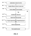
- FIG. 8 is a flow chart of one implementation of a method for identifying and compressing rarely used data.
- the present disclosure is directed to storage modules that provide the ability to identify and compress rarely used data.
- the described storage modules may monitor a host and/or a storage controller of the storage module accessing data stored in the storage module and identify rarely used data based on factors such as a number of times the host or the storage controller accesses data stored in the storage module without accessing data stored at a particular portion of the memory or a number of time a storage module exits and enters a hibernation state or a power off state (a power cycle) without the host or the storage controller accessing data stored at a particular portion of the memory.
- the storage module may identify one or more blocks of data stored at other portions of the memory that are rarely used.
- the storage controller may identify the one or more blocks of data stored at other locations that are rarely used by identifying data stored at memory locations that were last accessed at approximately the same time as the originally identified rarely used data.
- a storage module suitable for use in implementing aspects of the invention is shown in FIGS. 1-6 .
- a host system 100 of FIG. 1 stores data into and retrieves data from a storage module 102 .
- the storage module may be, for example, flash memory embedded within the host, such as in the form of a solid state disk (SSD) drive installed in a personal computer or an iNAND installed in a device.
- the storage module 102 may be in the form of a card, for example, that is removably connected to the host through mating parts 104 and 106 of a mechanical and electrical connector as illustrated in FIG. 1 .
- a flash memory configured for use as an internal or embedded SSD drive may look similar to the schematic of FIG. 1 , with the primary difference being the location of the storage module 102 internal to the host.
- SSD drives may be in the form of discrete modules that are drop-in replacements for rotating magnetic disk drives.
- the host system 100 of FIG. 1 may be viewed as having two major parts, in so far as the storage module 102 is concerned, made up of a combination of circuitry and software. They are an applications portion 108 and a driver portion 110 that interface with the storage module 102 .
- the applications portion 108 can include a processor 112 running word processing, graphics, control or other popular application software, as well as the file system 114 for managing data on the host 100 .
- the applications portion 108 includes the software that operates the camera to take and store pictures, the cellular telephone to make and receive calls, and the like.
- the storage module 102 of FIG. 1 may include non-volatile memory, such as flash memory 116 ; a storage controller 118 that both interfaces with the host 100 to which the storage module 102 is connected for passing data back and forth and controls the memory 116 ; and one or more data buffers 119 coupled with the storage controller 118 that the storage controller 118 utilizes to buffer data before storing the data to the flash memory 116 .
- the storage controller 118 may convert between logical addresses of data used by the host 100 and physical addresses of the flash memory 116 during data programming and reading.
- the flash memory 116 may include any number of memory die 120 and two memory die are shown in FIG. 1 simply by way of illustration.
- the storage controller 118 may include a front end 122 that interfaces with the host system, controller logic 124 for coordinating operation of the memory 116 , flash management logic 126 for internal memory management operations such as garbage collection, and one or more flash interface modules (FIMs) 128 to provide a communication interface between the controller with the flash memory 116 .
- controller logic 124 for coordinating operation of the memory 116
- flash management logic 126 for internal memory management operations such as garbage collection
- FIMs flash interface modules
- the storage controller 118 may be implemented on a single integrated circuit chip, such as an application specific integrated circuit (ASIC) such as shown in FIG. 2 .
- the processor 206 of the storage controller 118 may be configured as a multi-core and multi-thread processor capable of communicating separately with each of the respective memory banks 120 via a memory interface 204 having I/O ports for each of the respective banks 120 in the flash memory 116 .
- the storage controller 118 may include an internal clock 218 .
- the processor 206 communicates with an error correction code (ECC) module 214 , a RAM buffer 212 , a host interface 216 , and boot code ROM 210 via an internal data bus 202 .
- ECC error correction code
- Each die 120 in the flash memory 116 may contain an array of memory cells organized into multiple planes.
- FIG. 3 shows such planes 310 and 312 for simplicity but a greater number of planes, such as four or eight planes, may instead be used.
- the memory cell array of a memory bank may not be divided into planes.
- each plane has its own column control circuits 314 and 316 that are operable independently of each other.
- the circuits 314 and 316 receive addresses of their respective memory cell array from the address portion 306 of the system bus 302 , and decode them to address a specific one or more of respective bit lines 318 and 320 .
- the word lines 322 are addressed through row control circuits 324 in response to addresses received on the address bus 306 .
- Source voltage control circuits 326 and 328 are also connected with the respective planes, as are p-well voltage control circuits 330 and 332 . If the bank 300 is in the form of a memory chip with a single array of memory cells, and if two or more such chips exist in the system, data are transferred into and out of the planes 310 and 312 through respective data input/output circuits 334 and 336 that are connected with the data portion 304 of the system bus 302 .
- the circuits 334 and 336 provide for both programming data into the memory cells and for reading data from the memory cells of their respective planes, through lines 338 and 340 connected to the planes through respective column control circuits 314 and 316 .
- each memory chip also contains some controlling circuitry that executes commands from the controller 118 to perform such functions.
- Interface circuits 342 are connected to the control and status portion 308 of the system bus 302 .
- Commands from the controller 118 are provided to a state machine 344 that then provides specific control of other circuits in order to execute these commands.
- Control lines 346 - 354 connect the state machine 344 with these other circuits as shown in FIG. 3 .
- Status information from the state machine 344 is communicated over lines 356 to the interface 342 for transmission to the controller 118 over the bus portion 308 .
- a NAND architecture of the memory cell arrays 310 and 312 is discussed below, although other architectures, such as NOR, can be used instead.
- An example NAND array is illustrated by the circuit diagram of FIG. 4 , which is a portion of the memory cell array 310 of the memory bank 300 of FIG. 3 .
- a large number of global bit lines are provided, only four such lines 402 - 408 being shown in FIG. 4 a for simplicity of explanation.
- a number of series connected memory cell strings 410 - 424 are connected between one of these bit lines and a reference potential.
- a plurality of charge storage memory cells 426 - 432 are connected in series with select transistors 434 and 436 at either end of the string. When the select transistors of a string are rendered conductive, the string is connected between its bit line and the reference potential. One memory cell within that string is then programmed or read at a time.
- Word lines 438 - 444 of FIG. 4 a individually extend across the charge storage element of one memory cell in each of a number of strings of memory cells, and gates 446 and 450 control the states of the select transistors at each end of the strings.
- the memory cell strings that share common word and control gate lines 438 - 450 are made to form a block 452 of memory cells that are erased together. This block of cells contains the minimum number of cells that are physically erasable at one time.
- One row of memory cells, those along one of the word lines 438 - 444 are programmed at a time.
- the rows of a NAND array are programmed in a prescribed order, in this case beginning with the row along the word line 444 closest to the end of the strings connected to ground or another common potential.
- the row of memory cells along the word line 442 is programmed next, and so on, throughout the block 452 .
- the rows of a NAND array are not programmed in sequential order.
- a second block 454 is similar, its strings of memory cells being connected to the same global bit lines as the strings in the first block 452 but having a different set of word and control gate lines.
- the word and control gate lines are driven to their proper operating voltages by the row control circuits 324 . If there is more than one plane in the system, such as planes 1 and 2 of FIG. 3 , one memory architecture uses common word lines extending between them. There can alternatively be more than two planes that share common word lines. In other memory architectures, the word lines of individual planes are separately driven.
- the memory cells may be operated to store two levels of charge so that a single bit of data is stored in each cell. This is typically referred to as a binary or single level cell (SLC) memory. Alternatively, the memory cells may be operated to store more than two detectable levels of charge in each charge storage element or region, thereby to store more than one bit of data in each. This latter configuration is referred to as multi level cell (MLC) memory. Both types of memory cells may be used in a memory. For example, binary flash memory may be used for caching data and MLC memory may be used for longer term storage.
- the charge storage elements of the memory cells are most commonly conductive floating gates but may alternatively be non-conductive dielectric charge trapping material.
- each memory cell is configured to store four levels of charge corresponding to values of “11,” “01,” “10,” and “00.”
- Each bit of the two bits of data may represent a page bit of a lower page or a page bit of an upper page, where the lower page and upper page span across a series of memory cells sharing a common word line.
- the less significant bit of the two bits of data represents a page bit of a lower page and the more significant bit of the two bits of data represents a page bit of an upper page.
- FIG. 4 b illustrates one implementation of the four charge levels used to represent two bits of data in a memory cell.
- a value of “11” corresponds to an un-programmed state of the memory cell.
- the level of charge is increased to represent a value of “10” corresponding to a programmed state of the page bit of the lower page.
- FIG. 5 conceptually illustrates a multiple plane arrangement showing four planes 502 - 508 of memory cells. These planes 502 - 508 may be on a single die, on two die (two of the planes on each die) or on four separate die. Of course, other numbers of planes, such as 1, 2, 8, 16 or more may exist in each die of a system.
- the planes are individually divided into blocks of memory cells shown in FIG. 5 by rectangles, such as blocks 510 , 512 , 514 and 516 , located in respective planes 502 - 508 . There can be dozens or hundreds of blocks in each plane.
- a block of memory cells is the unit of erase, the smallest number of memory cells that are physically erasable together.
- the blocks are operated in larger metablock units.
- One block from each plane is logically linked together to form a metablock.
- the four blocks 510 - 516 are shown to form one metablock 518 . All of the cells within a metablock are typically erased together.
- the blocks used to form a metablock need not be restricted to the same relative locations within their respective planes, as is shown in a second metablock 520 made up of blocks 522 - 528 .
- the storage module can be operated with the ability to dynamically form metablocks of any or all of one, two or three blocks in different planes. This allows the size of the metablock to be more closely matched with the amount of data available for storage in one programming operation.
- the individual blocks are in turn divided for operational purposes into pages of memory cells, as illustrated in FIG. 6 .
- the memory cells of each of the blocks 510 - 516 are each divided into eight pages P 0 -P 7 .
- the page is the unit of data programming and reading within a block, containing the minimum amount of data that are programmed or read at one time.
- a page is formed of memory cells along a word line within a block.
- such pages within two or more blocks may be logically linked into metapages.
- a metapage 602 is illustrated in FIG.
- the metapage 602 for example, includes the page P 2 in each of the four blocks but the pages of a metapage need not necessarily have the same relative position within each of the blocks.
- the flash management layer in the controller firmware of the memory card may choose to allocate memory in terms of allocation units called logical groups. Writes that are less than a logical group size will result in the controller copying valid data stored at an original physical location to a new physical location in addition to the controller writing incoming data. This overhead decreases performance and endurance of the memory. In order to minimize this overhead, a group of memory is used as update blocks. An update block is usually a memory of better endurance than the data blocks. i.e, if the data blocks have MLC memory, the update blocks have SLC memory. Writes that are less than a logical group may result in the controller directing data into the update blocks, and after consolidation, the controller may copy data at a later point in time from the update block to one or more program data blocks.
- the controller performs these actions based on the fact that the update blocks are more durable and there is more possibility of collecting the entire logical group of data in the update blocks before writing into the data blocks, thus reducing overhead in the MLC memory. It is also more desirable to retain frequently written data blocks in the update block for similar reasons.
- a storage module may generally monitor access of a memory within the storage module and identify when a host or the storage controller itself accesses data stored at the memory of the storage module.
- the storage controller utilizes a timestamp such as an access counter and stores a value of the access counter at the time of identified access of data stored at a particular portion of the memory.
- the storage controller increases the access counter based on factors such as a number of times the host or the storage controller accesses the memory in general and/or a number of times the storage module enters or exits a hibernation state or a power off state. At a later time, the storage controller may compare a current value of the access counter with the stored associations between data stored at particular portions of the memory and previous access counter values to determine which portions of the memory are storing data that is rarely accessed.
- the storage controller may identify data stored at other portions of the memory that are also rarely accessed. For example, the storage controller may utilize the value of the access counter associated with the rarely accessed data to identify, based on recorded values of the access counter associated with data stored at other portions of the memory, data stored at other portions of the memory that is likely rarely accessed. The controller then compresses the identified rarely accessed data together.
- FIG. 7 is a method of one implementation for identifying access of a memory and associating the access with a timestamp such as an access counter.
- a storage controller monitors access of a first memory of the storage module.
- the first memory may be non-volatile memory such as a flash memory.
- Examples of an access may include a host reading data stored at the first memory, a host writing data to the first memory, the storage controller reading data stored at the first memory absent instructions from a host, and/or the storage controller writing data to the first memory absent instructions from a host.
- the storage controller may only consider the host or the storage controller writing data to the non-volatile memory to be an access and may not consider the host or the storage controller reading data from the non-volatile memory to be an access.
- the storage controller only considers a host reading data stored at the first memory or the host writing data to the first memory to be an access.
- the storage controller identifies an access of data stored at a first portion of first memory.
- a portion of the first memory may be a logical block address (LBA) of a memory, a page of memory, a block of memory, or any other division of memory that the storage controller is configured to operate with.
- LBA logical block address
- the storage controller may increment a value of an access counter, and at step 708 , the storage controller stores an association between a value of an access counter of the storage module and the data stored at the first portion of the first memory.
- the storage controller may utilize an access counter to record when data is accessed.
- the storage controller may increase a value of the access counter each time a host or the storage controller itself accesses the data; each time the storage module enters a hibernation state or a power off state; each time the storage module exits a hibernation state or a power off state; each powercycle (a time period between exiting and entering a hibernation state or a power off state) that a host or the storage controller access data; and/or any other point in time or action by the host or storage controller that would allow the storage controller to determine when data stored in a memory is aging.
- the storage controller stores the association between the value of the access counter of the storage module and the data stored at the first portion of the first memory in an Intermediate Access Table.
- a second memory such as a RAM of the storage controller, may store the Intermediate Access Table and the storage controller may periodically update an Access Time Table stored in the first memory with values from the Intermediate Access Table.
- the storage controller may store in an Intermediate Access Table stored in the second memory the association between a value of an access counter of the storage module and the data stored at the first portion of the first memory.
- the storage controller determines a need to update an Access Time Table stored in the first memory with values from the Intermediate Access Table stored in the second memory. For example, the storage controller may determine a need to update the Access Time Table with entries from the Intermediate Access Table each time the storage module receives a sleep/hibernation notification or a power off notification from a host instructing the storage module to enter a hibernation state or a power off state; after a defined number of changes in the Intermediate Access Table; after the value of the access counter increases by a defined amount since a last update of the Access Time Table; and/or any other factor that indicates to the storage controller that the Access Time Table stored in the first memory should be updated with values stored in that Intermediate Access Table stored in the second memory.
- the storage controller updates the Access Time Table stored in the first memory with one or more values from the Intermediate Access Table stored in the second memory. It will be appreciated by those of skill in the art that the storage controller may utilize two memories, such as RAM to store the Intermediate Access Table and non-volatile flash memory to store the Access Time Table, in order to increase performance of the storage module and reduce wear on the first memory.
- the above-described process is repeated with the storage controller recording associations between an access counter and an access of the first memory. Periodically, the storage controller reviews the stored associations to identify rarely used data based on the access counter associated with the last access of specific portions of memory.
- FIG. 8 is a flow chart of one implementation of a method for identifying and compressing rarely used data.
- the storage controller examines an entry in an Access Time Table associated with data stored at a portion of memory, and step 804 , the storage controller calculates a difference between a current value of an access counter and a value of the access counter that is associated with a most recent access of data stored at the portion of a memory.
- the storage controller determines whether the calculated difference exceeds a threshold that is set to indicate that data is rarely accessed (also known in the art as cold data). If the calculated difference does not exceed the threshold, the storage controller 808 determines that the data is regularly accessed. However, if the calculated difference does exceed the threshold, the storage controller determines at step 810 that the data is rarely accessed and that the probability that the host or storage controller will access the data in the future is low.
- a threshold that is set to indicate that data is rarely accessed (also known in the art as cold data). If the calculated difference does not exceed the threshold, the storage controller 808 determines that the data is regularly accessed. However, if the calculated difference does exceed the threshold, the storage controller determines at step 810 that the data is rarely accessed and that the probability that the host or storage controller will access the data in the future is low.
- the storage controller may search the Access Time Table for data stored at other portions of the memory whose most recent access is associated with a value of an access counter that is within a defined range of the value of the access counter that is associated with the data that the storage controller has already determined is rarely accessed.
- the storage controller may determine that data that was last accessed 3,000 power cycles ago is likely rarely accessed data. Further, the storage controller may determine that any data that was last accessed within 50 power cycles of the data that the storage controller has already determined to be rarely accessed data is also rarely accessed data and can be compressed together.
- the storage controller may determine that data that was last accessed 30,000,000 accesses ago is likely rarely accessed data. Further, the storage controller may determine that any data that was last accessed within 5,000 accesses of the data that the storage controller has already determined to be rarely accessed data is also rarely accessed data and can be compressed together.
- the storage controller compresses together the data stored in the portion of memory identified at step 810 and the data stored in the one or more portions of memory identified at step 812 .
- the storage controller stores the compressed data in the memory.
- the storage controller may limit a size of the compressed data stored at step 816 .
- the storage controller may define a cap such that a maximum size of the compressed data can be 1 MB. Accordingly, if the size of the data that can be compressed together exceeds 1 MB, the controller would divide the data into two or more chunks of no more than 1 MB and compress each chuck separately.
- FIGS. 1-8 illustrate systems and methods for identifying and compressing rarely used data.
- the described storage modules may monitor a host and/or a storage controller of the storage module accessing data stored in the storage module and identify rarely used data based on factors such as a number of times the host or the storage controller accesses data stored in the storage module without accessing data stored at a particular portion of the memory or a number of times a storage module exits and enters a hibernation state or a power off state (a power cycle) without the host or the storage controller accessing data stored at a particular portion of the memory.
- the storage module may identify one or more blocks of data stored at other portions of the memory that are rarely used.
- the storage controller may identify the one or more blocks of data stored at other locations that are rarely used by identifying data stored at memory locations that were last accessed at approximately the same time as the originally identified rarely used data.
- semiconductor memory devices such as those described in the present application may include volatile memory devices, such as dynamic random access memory (“DRAM”) or static random access memory (“SRAM”) devices, non-volatile memory devices, such as resistive random access memory (“ReRAM”), electrically erasable programmable read only memory (“EEPROM”), flash memory (which can also be considered a subset of EEPROM), ferroelectric random access memory (“FRAM”), and magnetoresistive random access memory (“MRAM”), and other semiconductor elements capable of storing information.
- volatile memory devices such as dynamic random access memory (“DRAM”) or static random access memory (“SRAM”) devices
- non-volatile memory devices such as resistive random access memory (“ReRAM”), electrically erasable programmable read only memory (“EEPROM”), flash memory (which can also be considered a subset of EEPROM), ferroelectric random access memory (“FRAM”), and magnetoresistive random access memory (“MRAM”), and other semiconductor elements capable of storing information.
- ReRAM resistive random access memory
- EEPROM
- the memory devices can be formed from passive and/or active elements, in any combinations.
- passive semiconductor memory elements include ReRAM device elements, which in some embodiments include a resistivity switching storage element, such as an anti-fuse, phase change material, etc., and optionally a steering element, such as a diode, etc.
- active semiconductor memory elements include EEPROM and flash memory device elements, which in some embodiments include elements containing a charge storage region, such as a floating gate, conductive nanoparticles, or a charge storage dielectric material.
- Multiple memory elements may be configured so that they are connected in series or so that each element is individually accessible.
- flash memory devices in a NAND configuration typically contain memory elements connected in series.
- a NAND memory array may be configured so that the array is composed of multiple strings of memory in which a string is composed of multiple memory elements sharing a single bit line and accessed as a group.
- memory elements may be configured so that each element is individually accessible, e.g., a NOR memory array.
- NAND and NOR memory configurations are exemplary, and memory elements may be otherwise configured.
- the semiconductor memory elements located within and/or over a substrate may be arranged in two or three dimensions, such as a two dimensional memory structure or a three dimensional memory structure.
- the semiconductor memory elements are arranged in a single plane or a single memory device level.
- memory elements are arranged in a plane (e.g., in an x-z direction plane) which extends substantially parallel to a major surface of a substrate that supports the memory elements.
- the substrate may be a wafer over or in which the layer of the memory elements are formed or it may be a carrier substrate which is attached to the memory elements after they are formed.
- the substrate may include a semiconductor such as silicon.
- the memory elements may be arranged in the single memory device level in an ordered array, such as in a plurality of rows and/or columns. However, the memory elements may be arrayed in non-regular or non-orthogonal configurations.
- the memory elements may each have two or more electrodes or contact lines, such as bit lines and word lines.
- a three dimensional memory array is arranged so that memory elements occupy multiple planes or multiple memory device levels, thereby forming a structure in three dimensions (i.e., in the x, y and z directions, where the y direction is substantially perpendicular and the x and z directions are substantially parallel to the major surface of the substrate).
- a three dimensional memory structure may be vertically arranged as a stack of multiple two dimensional memory device levels.
- a three dimensional memory array may be arranged as multiple vertical columns (e.g., columns extending substantially perpendicular to the major surface of the substrate, i.e., in the y direction) with each column having multiple memory elements in each column.
- the columns may be arranged in a two dimensional configuration, e.g., in an x-z plane, resulting in a three dimensional arrangement of memory elements with elements on multiple vertically stacked memory planes.
- Other configurations of memory elements in three dimensions can also constitute a three dimensional memory array.
- the memory elements may be coupled together to form a NAND string within a single horizontal (e.g., x-z) memory device levels.
- the memory elements may be coupled together to form a vertical NAND string that traverses across multiple horizontal memory device levels.
- Other three dimensional configurations can be envisioned wherein some NAND strings contain memory elements in a single memory level while other strings contain memory elements which span through multiple memory levels.
- Three dimensional memory arrays may also be designed in a NOR configuration and in a ReRAM configuration.
- a monolithic three dimensional memory array typically, one or more memory device levels are formed above a single substrate.
- the monolithic three dimensional memory array may also have one or more memory layers at least partially within the single substrate.
- the substrate may include a semiconductor such as silicon.
- the layers constituting each memory device level of the array are typically formed on the layers of the underlying memory device levels of the array.
- layers of adjacent memory device levels of a monolithic three dimensional memory array may be shared or have intervening layers between memory device levels.
- non-monolithic stacked memories can be constructed by forming memory levels on separate substrates and then stacking the memory levels atop each other. The substrates may be thinned or removed from the memory device levels before stacking, but as the memory device levels are initially formed over separate substrates, the resulting memory arrays are not monolithic three dimensional memory arrays. Further, multiple two dimensional memory arrays or three dimensional memory arrays (monolithic or non-monolithic) may be formed on separate chips and then packaged together to form a stacked-chip memory device.
- Associated circuitry is typically required for operation of the memory elements and for communication with the memory elements.
- memory devices may have circuitry used for controlling and driving memory elements to accomplish functions such as programming and reading.
- This associated circuitry may be on the same substrate as the memory elements and/or on a separate substrate.
- a controller for memory read-write operations may be located on a separate controller chip and/or on the same substrate as the memory elements.
Landscapes
- Engineering & Computer Science (AREA)
- Theoretical Computer Science (AREA)
- Physics & Mathematics (AREA)
- General Engineering & Computer Science (AREA)
- General Physics & Mathematics (AREA)
- Human Computer Interaction (AREA)
- Microelectronics & Electronic Packaging (AREA)
- Computer Hardware Design (AREA)
- Read Only Memory (AREA)
Abstract
Description
Claims (19)
Priority Applications (1)
| Application Number | Priority Date | Filing Date | Title |
|---|---|---|---|
| US14/288,992 US9110857B1 (en) | 2014-05-28 | 2014-05-28 | Systems and methods for identifying and compressing rarely used data |
Applications Claiming Priority (1)
| Application Number | Priority Date | Filing Date | Title |
|---|---|---|---|
| US14/288,992 US9110857B1 (en) | 2014-05-28 | 2014-05-28 | Systems and methods for identifying and compressing rarely used data |
Publications (1)
| Publication Number | Publication Date |
|---|---|
| US9110857B1 true US9110857B1 (en) | 2015-08-18 |
Family
ID=53786015
Family Applications (1)
| Application Number | Title | Priority Date | Filing Date |
|---|---|---|---|
| US14/288,992 Active US9110857B1 (en) | 2014-05-28 | 2014-05-28 | Systems and methods for identifying and compressing rarely used data |
Country Status (1)
| Country | Link |
|---|---|
| US (1) | US9110857B1 (en) |
Cited By (3)
| Publication number | Priority date | Publication date | Assignee | Title |
|---|---|---|---|---|
| US20160364178A1 (en) * | 2015-06-12 | 2016-12-15 | Nintendo Co., Ltd. | Information processing apparatus, information processing system, storage medium and information processing method |
| CN108733577A (en) * | 2017-04-21 | 2018-11-02 | 群联电子股份有限公司 | Memory management method, memory control circuit unit and memory storage device |
| US20250138729A1 (en) * | 2023-10-27 | 2025-05-01 | Dell Products L.P. | Method, electronic device, and computer program product for compressing data |
Citations (6)
| Publication number | Priority date | Publication date | Assignee | Title |
|---|---|---|---|---|
| US20060101084A1 (en) * | 2004-10-25 | 2006-05-11 | International Business Machines Corporation | Policy based data migration in a hierarchical data storage system |
| US20080307191A1 (en) * | 2007-06-07 | 2008-12-11 | International Business Machines Corporation | Method, system and computer program product for managing the storage of data |
| US20090019215A1 (en) * | 2004-03-30 | 2009-01-15 | Jin-Yub Lee | Method and device for performing cache reading |
| US20100169545A1 (en) * | 2008-12-25 | 2010-07-01 | Lian-Chun Lee | Host system and operating method thereof |
| US20110302352A1 (en) * | 2008-06-13 | 2011-12-08 | Samsung Electronics Co., Ltd. | Memory system and method of accessing a semiconductor memory device |
| US8187936B2 (en) | 2010-06-30 | 2012-05-29 | SanDisk Technologies, Inc. | Ultrahigh density vertical NAND memory device and method of making thereof |
-
2014
- 2014-05-28 US US14/288,992 patent/US9110857B1/en active Active
Patent Citations (6)
| Publication number | Priority date | Publication date | Assignee | Title |
|---|---|---|---|---|
| US20090019215A1 (en) * | 2004-03-30 | 2009-01-15 | Jin-Yub Lee | Method and device for performing cache reading |
| US20060101084A1 (en) * | 2004-10-25 | 2006-05-11 | International Business Machines Corporation | Policy based data migration in a hierarchical data storage system |
| US20080307191A1 (en) * | 2007-06-07 | 2008-12-11 | International Business Machines Corporation | Method, system and computer program product for managing the storage of data |
| US20110302352A1 (en) * | 2008-06-13 | 2011-12-08 | Samsung Electronics Co., Ltd. | Memory system and method of accessing a semiconductor memory device |
| US20100169545A1 (en) * | 2008-12-25 | 2010-07-01 | Lian-Chun Lee | Host system and operating method thereof |
| US8187936B2 (en) | 2010-06-30 | 2012-05-29 | SanDisk Technologies, Inc. | Ultrahigh density vertical NAND memory device and method of making thereof |
Non-Patent Citations (5)
| Title |
|---|
| Application as Filed for U.S. Appl. No. 14/133,979, filed Dec. 19, 2013, 121 pages. |
| Application as Filed for U.S. Appl. No. 14/136,103, filed Dec. 20, 2013, 56 pages. |
| Arya, P., "A Survey of 3D Nand Flash Memory", EECS Int'l Graduate Program, National Chiao Tung University, 2012, pp. 1-11. |
| Jang et al., "Vertical Cell Array using TCAT(Terabit Cell Array Transistor) Technology for Ultra High Density NAND Flash Memory," 2009 Symposium on VLSI Technology Digest of Technical Papers, pp. 192-193, 2009. |
| Nowak, E. et al., "Intrinsic Fluctuations in Vertical NAND Flash Memories", 2012 Symposium on VLSI Technology Digest of Technical Papers, 2012, pp. 21-22. |
Cited By (4)
| Publication number | Priority date | Publication date | Assignee | Title |
|---|---|---|---|---|
| US20160364178A1 (en) * | 2015-06-12 | 2016-12-15 | Nintendo Co., Ltd. | Information processing apparatus, information processing system, storage medium and information processing method |
| CN108733577A (en) * | 2017-04-21 | 2018-11-02 | 群联电子股份有限公司 | Memory management method, memory control circuit unit and memory storage device |
| US20250138729A1 (en) * | 2023-10-27 | 2025-05-01 | Dell Products L.P. | Method, electronic device, and computer program product for compressing data |
| US12443342B2 (en) * | 2023-10-27 | 2025-10-14 | Dell Products L.P. | Method, electronic device, and computer program product for compressing data based on segment IO counts of respective time segments for a storage area |
Similar Documents
| Publication | Publication Date | Title |
|---|---|---|
| US9778863B2 (en) | System and method for folding partial blocks into multi-level cell memory blocks | |
| US10929285B2 (en) | Storage system and method for generating a reverse map during a background operation and storing it in a host memory buffer | |
| US10102119B2 (en) | Garbage collection based on queued and/or selected write commands | |
| US10114562B2 (en) | Adaptive block allocation in nonvolatile memory | |
| US20160179399A1 (en) | System and Method for Selecting Blocks for Garbage Collection Based on Block Health | |
| US9478315B2 (en) | Bit error rate mapping in a memory system | |
| US9423971B2 (en) | Method and system for adaptively assigning logical block address read counters using a tree structure | |
| US9633738B1 (en) | Accelerated physical secure erase | |
| US9728262B2 (en) | Non-volatile memory systems with multi-write direction memory units | |
| US9037779B2 (en) | Systems and methods for performing variable flash wear leveling | |
| TW201621912A (en) | System and method for configuring and controlling non-volatile cache | |
| US9812209B2 (en) | System and method for memory integrated circuit chip write abort indication | |
| US9875049B2 (en) | Memory system and method for reducing peak current consumption | |
| US10629260B2 (en) | Dynamic management of programming states to improve endurance | |
| US9620201B1 (en) | Storage system and method for using hybrid blocks with sub-block erase operations | |
| US11334256B2 (en) | Storage system and method for boundary wordline data retention handling | |
| US9110857B1 (en) | Systems and methods for identifying and compressing rarely used data | |
| US9678684B2 (en) | Systems and methods for performing an adaptive sustain write in a memory system | |
| US10089226B2 (en) | Systems and methods for immediate physical erasure of data stored in a memory system in response to a user command | |
| US9507706B2 (en) | Memory system controller including a multi-resolution internal cache | |
| US12511074B2 (en) | Data storage device and method for classifying a set of continuous wordlines as an outlier band in an open block | |
| US12271261B2 (en) | Data storage device and method for host-assisted improved error recovery using a correlation factor | |
| US11429663B2 (en) | Storage system and method for host-assisted memory block color coding for faster media search | |
| US20250273278A1 (en) | Data Storage Device and Method for Managing a Hot Count Difference in Sub-Block Mode | |
| US20240079072A1 (en) | Data Storage Device and Method for Power on Reset and Read Error Handling |
Legal Events
| Date | Code | Title | Description |
|---|---|---|---|
| AS | Assignment |
Owner name: SANDISK TECHNOLOGIES INC., TEXAS Free format text: ASSIGNMENT OF ASSIGNORS INTEREST;ASSIGNORS:ROSTOKER, TAL;MARCU, ALON;REEL/FRAME:032978/0459 Effective date: 20140520 |
|
| STCF | Information on status: patent grant |
Free format text: PATENTED CASE |
|
| CC | Certificate of correction | ||
| AS | Assignment |
Owner name: SANDISK TECHNOLOGIES LLC, TEXAS Free format text: CHANGE OF NAME;ASSIGNOR:SANDISK TECHNOLOGIES INC;REEL/FRAME:038807/0948 Effective date: 20160516 |
|
| MAFP | Maintenance fee payment |
Free format text: PAYMENT OF MAINTENANCE FEE, 4TH YEAR, LARGE ENTITY (ORIGINAL EVENT CODE: M1551); ENTITY STATUS OF PATENT OWNER: LARGE ENTITY Year of fee payment: 4 |
|
| FEPP | Fee payment procedure |
Free format text: MAINTENANCE FEE REMINDER MAILED (ORIGINAL EVENT CODE: REM.); ENTITY STATUS OF PATENT OWNER: LARGE ENTITY |
|
| FEPP | Fee payment procedure |
Free format text: 7.5 YR SURCHARGE - LATE PMT W/IN 6 MO, LARGE ENTITY (ORIGINAL EVENT CODE: M1555); ENTITY STATUS OF PATENT OWNER: LARGE ENTITY |
|
| MAFP | Maintenance fee payment |
Free format text: PAYMENT OF MAINTENANCE FEE, 8TH YEAR, LARGE ENTITY (ORIGINAL EVENT CODE: M1552); ENTITY STATUS OF PATENT OWNER: LARGE ENTITY Year of fee payment: 8 |
|
| AS | Assignment |
Owner name: SANDISK TECHNOLOGIES, INC., CALIFORNIA Free format text: ASSIGNMENT OF ASSIGNORS INTEREST;ASSIGNOR:SANDISK TECHNOLOGIES LLC;REEL/FRAME:069796/0423 Effective date: 20241227 Owner name: SANDISK TECHNOLOGIES, INC., CALIFORNIA Free format text: ASSIGNMENT OF ASSIGNOR'S INTEREST;ASSIGNOR:SANDISK TECHNOLOGIES LLC;REEL/FRAME:069796/0423 Effective date: 20241227 |
|
| AS | Assignment |
Owner name: SANDISK TECHNOLOGIES, INC., CALIFORNIA Free format text: PARTIAL RELEASE OF SECURITY INTERESTS;ASSIGNOR:JPMORGAN CHASE BANK, N.A., AS AGENT;REEL/FRAME:071382/0001 Effective date: 20250424 Owner name: JPMORGAN CHASE BANK, N.A., AS COLLATERAL AGENT, ILLINOIS Free format text: SECURITY AGREEMENT;ASSIGNOR:SANDISK TECHNOLOGIES, INC.;REEL/FRAME:071050/0001 Effective date: 20250424 |