US9105798B2 - Preparation of CIGS absorber layers using coated semiconductor nanoparticle and nanowire networks - Google Patents
Preparation of CIGS absorber layers using coated semiconductor nanoparticle and nanowire networks Download PDFInfo
- Publication number
- US9105798B2 US9105798B2 US13/893,756 US201313893756A US9105798B2 US 9105798 B2 US9105798 B2 US 9105798B2 US 201313893756 A US201313893756 A US 201313893756A US 9105798 B2 US9105798 B2 US 9105798B2
- Authority
- US
- United States
- Prior art keywords
- cigs
- solution
- ink
- nanoparticles
- precursor
- Prior art date
- Legal status (The legal status is an assumption and is not a legal conclusion. Google has not performed a legal analysis and makes no representation as to the accuracy of the status listed.)
- Active, expires
Links
- 239000002105 nanoparticle Substances 0.000 title claims abstract description 63
- 239000002070 nanowire Substances 0.000 title claims abstract description 46
- 239000006096 absorbing agent Substances 0.000 title claims abstract description 6
- 239000004065 semiconductor Substances 0.000 title abstract description 4
- 238000000034 method Methods 0.000 claims abstract description 66
- 239000002243 precursor Substances 0.000 claims abstract description 60
- 230000002776 aggregation Effects 0.000 claims abstract description 11
- 238000004220 aggregation Methods 0.000 claims abstract description 11
- 229910052733 gallium Inorganic materials 0.000 claims abstract description 11
- 150000003839 salts Chemical class 0.000 claims abstract description 10
- 239000002184 metal Substances 0.000 claims abstract description 8
- 229910052751 metal Inorganic materials 0.000 claims abstract description 8
- OKTJSMMVPCPJKN-UHFFFAOYSA-N Carbon Chemical compound [C] OKTJSMMVPCPJKN-UHFFFAOYSA-N 0.000 claims abstract description 6
- QTBSBXVTEAMEQO-UHFFFAOYSA-M Acetate Chemical compound CC([O-])=O QTBSBXVTEAMEQO-UHFFFAOYSA-M 0.000 claims abstract description 4
- 229910001510 metal chloride Inorganic materials 0.000 claims abstract description 4
- 239000000758 substrate Substances 0.000 claims description 30
- 238000004544 sputter deposition Methods 0.000 claims description 26
- 239000000843 powder Substances 0.000 claims description 23
- 238000005507 spraying Methods 0.000 claims description 19
- 239000011521 glass Substances 0.000 claims description 18
- 238000010438 heat treatment Methods 0.000 claims description 16
- 238000003756 stirring Methods 0.000 claims description 16
- 239000002904 solvent Substances 0.000 claims description 14
- 238000000224 chemical solution deposition Methods 0.000 claims description 13
- 230000002194 synthesizing effect Effects 0.000 claims description 13
- OKKJLVBELUTLKV-UHFFFAOYSA-N Methanol Chemical compound OC OKKJLVBELUTLKV-UHFFFAOYSA-N 0.000 claims description 12
- 238000001704 evaporation Methods 0.000 claims description 12
- 239000011669 selenium Substances 0.000 claims description 12
- 239000007921 spray Substances 0.000 claims description 12
- 239000000654 additive Substances 0.000 claims description 10
- 238000000151 deposition Methods 0.000 claims description 9
- 230000000694 effects Effects 0.000 claims description 9
- 239000002562 thickening agent Substances 0.000 claims description 9
- 239000000203 mixture Substances 0.000 claims description 8
- 230000008719 thickening Effects 0.000 claims description 8
- UMGDCJDMYOKAJW-UHFFFAOYSA-N thiourea Chemical compound NC(N)=S UMGDCJDMYOKAJW-UHFFFAOYSA-N 0.000 claims description 8
- 230000008859 change Effects 0.000 claims description 7
- 229910052802 copper Inorganic materials 0.000 claims description 7
- 238000001035 drying Methods 0.000 claims description 7
- 229910052738 indium Inorganic materials 0.000 claims description 7
- 239000002245 particle Substances 0.000 claims description 7
- 239000011858 nanopowder Substances 0.000 claims description 6
- XLYOFNOQVPJJNP-UHFFFAOYSA-N water Chemical compound O XLYOFNOQVPJJNP-UHFFFAOYSA-N 0.000 claims description 6
- 150000002500 ions Chemical class 0.000 claims description 5
- CSCPPACGZOOCGX-UHFFFAOYSA-N Acetone Chemical compound CC(C)=O CSCPPACGZOOCGX-UHFFFAOYSA-N 0.000 claims description 4
- LFQSCWFLJHTTHZ-UHFFFAOYSA-N Ethanol Chemical compound CCO LFQSCWFLJHTTHZ-UHFFFAOYSA-N 0.000 claims description 4
- 239000001856 Ethyl cellulose Substances 0.000 claims description 4
- ZZSNKZQZMQGXPY-UHFFFAOYSA-N Ethyl cellulose Chemical compound CCOCC1OC(OC)C(OCC)C(OCC)C1OC1C(O)C(O)C(OC)C(CO)O1 ZZSNKZQZMQGXPY-UHFFFAOYSA-N 0.000 claims description 4
- 229910003310 Ni-Al Inorganic materials 0.000 claims description 4
- XSQUKJJJFZCRTK-UHFFFAOYSA-N Urea Natural products NC(N)=O XSQUKJJJFZCRTK-UHFFFAOYSA-N 0.000 claims description 4
- 239000007822 coupling agent Substances 0.000 claims description 4
- 239000002270 dispersing agent Substances 0.000 claims description 4
- 229920001249 ethyl cellulose Polymers 0.000 claims description 4
- 235000019325 ethyl cellulose Nutrition 0.000 claims description 4
- 239000012456 homogeneous solution Substances 0.000 claims description 4
- PSCMQHVBLHHWTO-UHFFFAOYSA-K indium(iii) chloride Chemical compound Cl[In](Cl)Cl PSCMQHVBLHHWTO-UHFFFAOYSA-K 0.000 claims description 4
- 238000002156 mixing Methods 0.000 claims description 4
- 239000003960 organic solvent Substances 0.000 claims description 4
- 238000005303 weighing Methods 0.000 claims description 4
- BUGBHKTXTAQXES-UHFFFAOYSA-N Selenium Chemical compound [Se] BUGBHKTXTAQXES-UHFFFAOYSA-N 0.000 claims description 3
- 229910002804 graphite Inorganic materials 0.000 claims description 3
- 239000010439 graphite Substances 0.000 claims description 3
- FAXDZWQIWUSWJH-UHFFFAOYSA-N 3-methoxypropan-1-amine Chemical compound COCCCN FAXDZWQIWUSWJH-UHFFFAOYSA-N 0.000 claims description 2
- 229910005267 GaCl3 Inorganic materials 0.000 claims description 2
- 229910017906 NH3H2O Inorganic materials 0.000 claims description 2
- 229910052782 aluminium Inorganic materials 0.000 claims description 2
- 238000009835 boiling Methods 0.000 claims description 2
- QCUOBSQYDGUHHT-UHFFFAOYSA-L cadmium sulfate Chemical compound [Cd+2].[O-]S([O-])(=O)=O QCUOBSQYDGUHHT-UHFFFAOYSA-L 0.000 claims description 2
- 229910000369 cadmium(II) sulfate Inorganic materials 0.000 claims description 2
- 238000011010 flushing procedure Methods 0.000 claims description 2
- UPWPDUACHOATKO-UHFFFAOYSA-K gallium trichloride Chemical compound Cl[Ga](Cl)Cl UPWPDUACHOATKO-UHFFFAOYSA-K 0.000 claims description 2
- 238000011068 loading method Methods 0.000 claims description 2
- 229910052759 nickel Inorganic materials 0.000 claims description 2
- 239000006259 organic additive Substances 0.000 claims description 2
- 239000010453 quartz Substances 0.000 claims description 2
- VYPSYNLAJGMNEJ-UHFFFAOYSA-N silicon dioxide Inorganic materials O=[Si]=O VYPSYNLAJGMNEJ-UHFFFAOYSA-N 0.000 claims description 2
- 239000007787 solid Substances 0.000 claims description 2
- RBNWAMSGVWEHFP-UHFFFAOYSA-N trans-p-Menthane-1,8-diol Chemical compound CC(C)(O)C1CCC(C)(O)CC1 RBNWAMSGVWEHFP-UHFFFAOYSA-N 0.000 claims description 2
- 238000005406 washing Methods 0.000 claims description 2
- 238000001816 cooling Methods 0.000 claims 5
- MPTQRFCYZCXJFQ-UHFFFAOYSA-L copper(II) chloride dihydrate Chemical compound O.O.[Cl-].[Cl-].[Cu+2] MPTQRFCYZCXJFQ-UHFFFAOYSA-L 0.000 claims 1
- GCLGEJMYGQKIIW-UHFFFAOYSA-H sodium hexametaphosphate Chemical compound [Na]OP1(=O)OP(=O)(O[Na])OP(=O)(O[Na])OP(=O)(O[Na])OP(=O)(O[Na])OP(=O)(O[Na])O1 GCLGEJMYGQKIIW-UHFFFAOYSA-H 0.000 claims 1
- 235000019982 sodium hexametaphosphate Nutrition 0.000 claims 1
- 230000015572 biosynthetic process Effects 0.000 abstract description 8
- 239000011261 inert gas Substances 0.000 abstract description 5
- 239000003795 chemical substances by application Substances 0.000 abstract description 4
- 229910052799 carbon Inorganic materials 0.000 abstract description 3
- 238000004140 cleaning Methods 0.000 abstract description 3
- 230000008569 process Effects 0.000 description 22
- 239000010408 film Substances 0.000 description 19
- 239000000976 ink Substances 0.000 description 15
- 239000010949 copper Substances 0.000 description 7
- 238000010586 diagram Methods 0.000 description 7
- 238000004519 manufacturing process Methods 0.000 description 7
- 239000010409 thin film Substances 0.000 description 7
- 239000007789 gas Substances 0.000 description 6
- 238000006243 chemical reaction Methods 0.000 description 5
- 238000003786 synthesis reaction Methods 0.000 description 5
- ZWEHNKRNPOVVGH-UHFFFAOYSA-N 2-Butanone Chemical compound CCC(C)=O ZWEHNKRNPOVVGH-UHFFFAOYSA-N 0.000 description 4
- -1 gallium selenides Chemical class 0.000 description 4
- 239000000463 material Substances 0.000 description 4
- 230000008901 benefit Effects 0.000 description 3
- 239000011230 binding agent Substances 0.000 description 3
- 230000008021 deposition Effects 0.000 description 3
- 238000005516 engineering process Methods 0.000 description 3
- OAKJQQAXSVQMHS-UHFFFAOYSA-N Hydrazine Chemical compound NN OAKJQQAXSVQMHS-UHFFFAOYSA-N 0.000 description 2
- 239000012298 atmosphere Substances 0.000 description 2
- 230000004888 barrier function Effects 0.000 description 2
- 239000011258 core-shell material Substances 0.000 description 2
- 230000004048 modification Effects 0.000 description 2
- 238000012986 modification Methods 0.000 description 2
- 238000013341 scale-up Methods 0.000 description 2
- 231100000331 toxic Toxicity 0.000 description 2
- 230000002588 toxic effect Effects 0.000 description 2
- DKIDEFUBRARXTE-UHFFFAOYSA-N 3-mercaptopropanoic acid Chemical compound OC(=O)CCS DKIDEFUBRARXTE-UHFFFAOYSA-N 0.000 description 1
- 241001279686 Allium moly Species 0.000 description 1
- RYGMFSIKBFXOCR-UHFFFAOYSA-N Copper Chemical compound [Cu] RYGMFSIKBFXOCR-UHFFFAOYSA-N 0.000 description 1
- 229910021592 Copper(II) chloride Inorganic materials 0.000 description 1
- 240000005636 Dryobalanops aromatica Species 0.000 description 1
- UFHFLCQGNIYNRP-UHFFFAOYSA-N Hydrogen Chemical compound [H][H] UFHFLCQGNIYNRP-UHFFFAOYSA-N 0.000 description 1
- DGAQECJNVWCQMB-PUAWFVPOSA-M Ilexoside XXIX Chemical compound C[C@@H]1CC[C@@]2(CC[C@@]3(C(=CC[C@H]4[C@]3(CC[C@@H]5[C@@]4(CC[C@@H](C5(C)C)OS(=O)(=O)[O-])C)C)[C@@H]2[C@]1(C)O)C)C(=O)O[C@H]6[C@@H]([C@H]([C@@H]([C@H](O6)CO)O)O)O.[Na+] DGAQECJNVWCQMB-PUAWFVPOSA-M 0.000 description 1
- 238000010521 absorption reaction Methods 0.000 description 1
- 239000003963 antioxidant agent Substances 0.000 description 1
- 235000006708 antioxidants Nutrition 0.000 description 1
- 230000005540 biological transmission Effects 0.000 description 1
- 239000000919 ceramic Substances 0.000 description 1
- DVRDHUBQLOKMHZ-UHFFFAOYSA-N chalcopyrite Chemical compound [S-2].[S-2].[Fe+2].[Cu+2] DVRDHUBQLOKMHZ-UHFFFAOYSA-N 0.000 description 1
- 229910052951 chalcopyrite Inorganic materials 0.000 description 1
- 238000001311 chemical methods and process Methods 0.000 description 1
- 239000003153 chemical reaction reagent Substances 0.000 description 1
- 231100000481 chemical toxicant Toxicity 0.000 description 1
- 238000010549 co-Evaporation Methods 0.000 description 1
- 238000000576 coating method Methods 0.000 description 1
- 239000000084 colloidal system Substances 0.000 description 1
- 238000010276 construction Methods 0.000 description 1
- 229910021419 crystalline silicon Inorganic materials 0.000 description 1
- ZZEMEJKDTZOXOI-UHFFFAOYSA-N digallium;selenium(2-) Chemical compound [Ga+3].[Ga+3].[Se-2].[Se-2].[Se-2] ZZEMEJKDTZOXOI-UHFFFAOYSA-N 0.000 description 1
- 239000003995 emulsifying agent Substances 0.000 description 1
- 239000002360 explosive Substances 0.000 description 1
- XLYOFNOQVPJJNP-ZSJDYOACSA-N heavy water Substances [2H]O[2H] XLYOFNOQVPJJNP-ZSJDYOACSA-N 0.000 description 1
- 229910052739 hydrogen Inorganic materials 0.000 description 1
- 239000001257 hydrogen Substances 0.000 description 1
- APFVFJFRJDLVQX-UHFFFAOYSA-N indium atom Chemical compound [In] APFVFJFRJDLVQX-UHFFFAOYSA-N 0.000 description 1
- AKUCEXGLFUSJCD-UHFFFAOYSA-N indium(3+);selenium(2-) Chemical compound [Se-2].[Se-2].[Se-2].[In+3].[In+3] AKUCEXGLFUSJCD-UHFFFAOYSA-N 0.000 description 1
- 239000004615 ingredient Substances 0.000 description 1
- 230000031700 light absorption Effects 0.000 description 1
- 239000007791 liquid phase Substances 0.000 description 1
- 229910003455 mixed metal oxide Inorganic materials 0.000 description 1
- 239000003973 paint Substances 0.000 description 1
- 239000004014 plasticizer Substances 0.000 description 1
- 239000003755 preservative agent Substances 0.000 description 1
- 238000007639 printing Methods 0.000 description 1
- 230000035484 reaction time Effects 0.000 description 1
- 230000009467 reduction Effects 0.000 description 1
- 238000011946 reduction process Methods 0.000 description 1
- SPVXKVOXSXTJOY-UHFFFAOYSA-N selane Chemical compound [SeH2] SPVXKVOXSXTJOY-UHFFFAOYSA-N 0.000 description 1
- 229910000058 selane Inorganic materials 0.000 description 1
- IRPLSAGFWHCJIQ-UHFFFAOYSA-N selanylidenecopper Chemical compound [Se]=[Cu] IRPLSAGFWHCJIQ-UHFFFAOYSA-N 0.000 description 1
- 150000003346 selenoethers Chemical class 0.000 description 1
- 239000011734 sodium Substances 0.000 description 1
- 229910052708 sodium Inorganic materials 0.000 description 1
- 229910001220 stainless steel Inorganic materials 0.000 description 1
- 239000010935 stainless steel Substances 0.000 description 1
- 239000007858 starting material Substances 0.000 description 1
- 239000000126 substance Substances 0.000 description 1
- 239000004094 surface-active agent Substances 0.000 description 1
- 239000003440 toxic substance Substances 0.000 description 1
Images


Classifications
-
- H01L31/18—
-
- H—ELECTRICITY
- H10—SEMICONDUCTOR DEVICES; ELECTRIC SOLID-STATE DEVICES NOT OTHERWISE PROVIDED FOR
- H10F—INORGANIC SEMICONDUCTOR DEVICES SENSITIVE TO INFRARED RADIATION, LIGHT, ELECTROMAGNETIC RADIATION OF SHORTER WAVELENGTH OR CORPUSCULAR RADIATION
- H10F71/00—Manufacture or treatment of devices covered by this subclass
-
- H01L31/0322—
-
- H—ELECTRICITY
- H10—SEMICONDUCTOR DEVICES; ELECTRIC SOLID-STATE DEVICES NOT OTHERWISE PROVIDED FOR
- H10F—INORGANIC SEMICONDUCTOR DEVICES SENSITIVE TO INFRARED RADIATION, LIGHT, ELECTROMAGNETIC RADIATION OF SHORTER WAVELENGTH OR CORPUSCULAR RADIATION
- H10F10/00—Individual photovoltaic cells, e.g. solar cells
- H10F10/10—Individual photovoltaic cells, e.g. solar cells having potential barriers
- H10F10/16—Photovoltaic cells having only PN heterojunction potential barriers
- H10F10/167—Photovoltaic cells having only PN heterojunction potential barriers comprising Group I-III-VI materials, e.g. CdS/CuInSe2 [CIS] heterojunction photovoltaic cells
-
- H—ELECTRICITY
- H10—SEMICONDUCTOR DEVICES; ELECTRIC SOLID-STATE DEVICES NOT OTHERWISE PROVIDED FOR
- H10F—INORGANIC SEMICONDUCTOR DEVICES SENSITIVE TO INFRARED RADIATION, LIGHT, ELECTROMAGNETIC RADIATION OF SHORTER WAVELENGTH OR CORPUSCULAR RADIATION
- H10F77/00—Constructional details of devices covered by this subclass
- H10F77/10—Semiconductor bodies
- H10F77/12—Active materials
- H10F77/126—Active materials comprising only Group I-III-VI chalcopyrite materials, e.g. CuInSe2, CuGaSe2 or CuInGaSe2 [CIGS]
-
- C—CHEMISTRY; METALLURGY
- C09—DYES; PAINTS; POLISHES; NATURAL RESINS; ADHESIVES; COMPOSITIONS NOT OTHERWISE PROVIDED FOR; APPLICATIONS OF MATERIALS NOT OTHERWISE PROVIDED FOR
- C09D—COATING COMPOSITIONS, e.g. PAINTS, VARNISHES OR LACQUERS; FILLING PASTES; CHEMICAL PAINT OR INK REMOVERS; INKS; CORRECTING FLUIDS; WOODSTAINS; PASTES OR SOLIDS FOR COLOURING OR PRINTING; USE OF MATERIALS THEREFOR
- C09D11/00—Inks
- C09D11/02—Printing inks
-
- Y—GENERAL TAGGING OF NEW TECHNOLOGICAL DEVELOPMENTS; GENERAL TAGGING OF CROSS-SECTIONAL TECHNOLOGIES SPANNING OVER SEVERAL SECTIONS OF THE IPC; TECHNICAL SUBJECTS COVERED BY FORMER USPC CROSS-REFERENCE ART COLLECTIONS [XRACs] AND DIGESTS
- Y02—TECHNOLOGIES OR APPLICATIONS FOR MITIGATION OR ADAPTATION AGAINST CLIMATE CHANGE
- Y02E—REDUCTION OF GREENHOUSE GAS [GHG] EMISSIONS, RELATED TO ENERGY GENERATION, TRANSMISSION OR DISTRIBUTION
- Y02E10/00—Energy generation through renewable energy sources
- Y02E10/50—Photovoltaic [PV] energy
- Y02E10/541—CuInSe2 material PV cells
-
- Y—GENERAL TAGGING OF NEW TECHNOLOGICAL DEVELOPMENTS; GENERAL TAGGING OF CROSS-SECTIONAL TECHNOLOGIES SPANNING OVER SEVERAL SECTIONS OF THE IPC; TECHNICAL SUBJECTS COVERED BY FORMER USPC CROSS-REFERENCE ART COLLECTIONS [XRACs] AND DIGESTS
- Y02—TECHNOLOGIES OR APPLICATIONS FOR MITIGATION OR ADAPTATION AGAINST CLIMATE CHANGE
- Y02E—REDUCTION OF GREENHOUSE GAS [GHG] EMISSIONS, RELATED TO ENERGY GENERATION, TRANSMISSION OR DISTRIBUTION
- Y02E10/00—Energy generation through renewable energy sources
- Y02E10/50—Photovoltaic [PV] energy
- Y02E10/544—Solar cells from Group III-V materials
-
- Y—GENERAL TAGGING OF NEW TECHNOLOGICAL DEVELOPMENTS; GENERAL TAGGING OF CROSS-SECTIONAL TECHNOLOGIES SPANNING OVER SEVERAL SECTIONS OF THE IPC; TECHNICAL SUBJECTS COVERED BY FORMER USPC CROSS-REFERENCE ART COLLECTIONS [XRACs] AND DIGESTS
- Y02—TECHNOLOGIES OR APPLICATIONS FOR MITIGATION OR ADAPTATION AGAINST CLIMATE CHANGE
- Y02P—CLIMATE CHANGE MITIGATION TECHNOLOGIES IN THE PRODUCTION OR PROCESSING OF GOODS
- Y02P70/00—Climate change mitigation technologies in the production process for final industrial or consumer products
- Y02P70/50—Manufacturing or production processes characterised by the final manufactured product
Definitions
- the present invention relates to a method synthesizing Cu(In,Ga)S 2 nanoparticles/wires based on metal salts.
- a CIGS thin film is prepared by the formation of semiconductor nanoparticle and nanowire networks and selenization for a light absorption layer of photovoltaic devices.
- Chalcopyrite CuInGaSe 2 CIGSe is a direct band gap semiconductor and has an exceptionally high absorption coefficient of more than 10 5 /cm for 1.5 eV and higher energy photons. According to the recent report from the ZSW, a solar cell based on CIGSe has reached a power conversion efficiency of 20.3%, which is comparable with the energy conversion efficiency of crystalline Si solar cells. Decent conversion efficiency and high chemical stability of CIGSe make itself a promising p-type material for thin film photovoltaic devices.
- Vacuum and non-vacuum technologies are the two main methods of preparing CIGSe thin films.
- Vacuum-based processes including co-evaporation and sputtering, which have been successfully applied in commercial production lines.
- the high cost and complexity of vacuum-based fabrication process become barriers to affordable commercial modules.
- An efficient non-vacuum printing process has the potential to overcome this barrier.
- the low cost technique is inherently suitable for large-scale applications and may benefit from established industries of coatings, paints, inks, electronic ceramics and colloidal systems.
- deposition at atmospheric environment offers an opportunity for the deposition of absorber materials at large scale with high throughput. This provides a potential cost advantage over conventional fabrication process that involves expensive vacuum equipment.
- Kapur et at (U.S. Pat. No. 6,127,202) describe a method for fabricating a CIGSe solar cell based upon the solution-based deposition of a source material comprised of mechanically milled, oxide-containing, sub-micron sized particles, while Eberspacher and Pauls (U.S. Pat. No. 6,268,014); Published U.S. Patent Application No. 2002/0006470) describe the forming of mixed metal oxide, sub-micron sized particles by pyrolizing droplets of a solution, then ultrasonically spraying the resulting particles onto a substrate.
- the high-temperature hydrogen reduction step is potentially explosive and requires substantial time and energy.
- highly toxic H 2 Se gas atmosphere is requested in the selenization process.
- Byoung Koun Min in Published U.S. Patent Application No. 2012/0080091 A1 also involves the reduction process.
- Fuqiang Huang in Published U.S. Patent Application No. 2011/0008927 A1 gets a 14.6% high efficiency employing a non-vacuum liquid-phase chemical technique.
- Nanosolar Inc. in Published U.S. Patent Application No. 2008/0149176 has used binary copper selenide and indium/gallium selenides nanoparticles as starting materials to fabricate 14% thin film CIGSe solar cells.
- Single metallic nanoparticles are the simplest form one could design.
- the structure of nanoparticles used by Nanosolar has a core-shell structure. Copper nanoparticles serve as the cores which are coated with IIIA-VIA shells such as indium selenide, gallium selenide etc.
- selenide nanoparticles are dispersed in organic solution which may contain various ingredients including solvents, surfactants, binders, emulsifiers, thickening agents, film conditioners, anti-oxidants, flow and leveling agents, plasticizers and preservatives.
- organic solution may contain various ingredients including solvents, surfactants, binders, emulsifiers, thickening agents, film conditioners, anti-oxidants, flow and leveling agents, plasticizers and preservatives.
- the subject invention presents a facile way to synthesize soluble CIGS nanoparticles/wires at room temperature under non-vacuum condition and the reaction can finish in 5 minutes.
- high quality Cu(In,Ga)SSe 2 (CIGSS) thin films are prepared.
- the effective solar cells based on the non-vacuum method in accordance with the invention are also achieved.
- the invention allows the drawbacks of the known non-vacuum techniques to be eliminated.
- the invention provides a method for preparing CIGSS absorber layers by using a metal salt, thickening and binding agents to form uniform nanoparticle and nanowire networks and to provide a finished high quality CIGSS film after selenization, in which:
- CIGS nanoparticles and nanowires are produced based on using a metal salt such as metal chloride and acetate at room temperature without inert gas protection;
- a CIGS precursor layer is coated on a Mo glass substrate by ultrasonic spraying of the CIGS nanoparticle and nanowire solution;
- a clean CIGS precursor layer is obtained by cleaning the residue salts and carbon agents at an increased temperature above 200° C.;
- High quality CIGSS film is fabricated after selenizing the pretreated precursor layer at a temperature above 500° C.
- FIG. 1 is a diagram of the fabrication process of CIGS PV device
- FIG. 2 is a diagram of the synthesis process of CIGS nanoparticles/wires
- FIG. 3 is a detailed schematic diagram of the process of preparing CIGSS solar cells based on non-vacuum method.
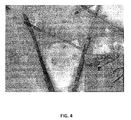
- FIG. 4 is the TEM and the picture of CIGS nanoparticles/wires
- FIG. 5 is the TEM of decomposed CIGS nanowires
- FIG. 6 is a diagram of the selenization temperature profile
- FIG. 7 is cross-sectional TEM of CIGSS films.
- FIG. 8 is the structure diagram and picture of CIGSS device.
- FIG. 1 shows the fabrication process of CIGSS photo-voltaic (“PV”) device.
- CIGS nanoparticles/wires have been synthesized using the low-cost solution route under atmospheric conditions in accordance with the present invention.
- the approach is simpler and less costly than any other non-vacuum methods with the following advantages:
- nanoparticles (3) Formation of amorphous and soluble nanoparticles/wires.
- the nanoparticles can be deposited on various substrates and turn into uniform thin films at low temperature ( ⁇ 350° C.);
- the amorphous CIGS nanoparticles fabricated in our invention melt under low temperature (even below 180V) and crystallize to various sizes of nanoparticles with increasing temperature (above 200° C.).
- Ultrasonic spraying CIGS ink on Mo glass substrate using ultrasonic spray to reduce the aggregation effect of CIGS nanoparticles/nanowires and obtaining uniform CIGS precursor films.
- the process of ultrasonic spraying CIGS-based ink on Mo-coated glass substrate, such as a glass substrate, includes the following steps illustrated in FIG. 3 :
- Preparing CIGSS device uses typical chemical bath deposition and sputtering and evaporating route.
- the whole process of fabricating CIGSS PV device includes the following detailed steps:
- a thickening solution B by: Adding Ethylcellulose (EC) (e.g. 0.3 g) into Terpinol (e.g. 10 mL), stirring overnight and heating to a temperature up to 200° C. until it is completely dissolved.
- Ethylcellulose e.g. 0.3 g
- Terpinol e.g. 10 mL
- CIGS dried powder e.g. 3.0 g
- solvent methyl ethyl ketone (“MEK”) e.g. 70 mL
- PEG e.g. 30 mL
- SHMP sodium hexametaphophate
- monodispersed CIGS ink e.g. 100 mL
- Ts under 300° C. (e.g. 100° C.);
- D less than 150 mm (e.g. 90 mm);
- the procedures of heating treatment are described.
- the process of heat treatment includes the following steps:
- FIG. 5 shown the nanowires begin to decompose under 150° C.
- the temperature is increased up to 500° C. (e.g. 350° C.) and held for half an hour, which will remove all the organic solvents and additives, finally the color changes to a deep black.
- FIG. 6 shows the selenization temperature profile.
- FIG. 8 shows the structure diagram and picture of CIGSS device made in accordance with the invention.
- the invention allows the drawbacks of the known non-vacuum techniques to be eliminated.
- the invention provides a method for preparing CIGSS absorber layers by using a metal salt, thickening and binding agents to form uniform nanoparticle and nanowire networks and to provide a finished high quality CIGSS film after selenization, in which:
- CIGS nanoparticles and nanowires are produced based on using a metal salt such as metal chloride and acetate at room temperature without inert gas protection;
- a CIGS precursor layer is coated on a Mo glass substrate by ultrasonic sprying of the CIGS nanoparticle and nanowire solution;
- a clean CIGS precursor layer is obtained by cleaning the residue salts and carbon agents at an increased temperature above 200° C.
- High quality CIGSS film is fabricated after selenizing the pretreated precursor layer at a temperature above 400° C.
Landscapes
- Engineering & Computer Science (AREA)
- Manufacturing & Machinery (AREA)
- Photovoltaic Devices (AREA)
Abstract
Description
Claims (14)
Priority Applications (2)
| Application Number | Priority Date | Filing Date | Title |
|---|---|---|---|
| US13/893,756 US9105798B2 (en) | 2013-05-14 | 2013-05-14 | Preparation of CIGS absorber layers using coated semiconductor nanoparticle and nanowire networks |
| US14/048,285 US20140342496A1 (en) | 2013-05-14 | 2013-12-16 | Preparation of cigs absorber layers using coated semiconductor nanoparticle and nanowire networks |
Applications Claiming Priority (1)
| Application Number | Priority Date | Filing Date | Title |
|---|---|---|---|
| US13/893,756 US9105798B2 (en) | 2013-05-14 | 2013-05-14 | Preparation of CIGS absorber layers using coated semiconductor nanoparticle and nanowire networks |
Related Child Applications (1)
| Application Number | Title | Priority Date | Filing Date |
|---|---|---|---|
| US14/048,285 Continuation US20140342496A1 (en) | 2013-05-14 | 2013-12-16 | Preparation of cigs absorber layers using coated semiconductor nanoparticle and nanowire networks |
Publications (2)
| Publication Number | Publication Date |
|---|---|
| US20140342495A1 US20140342495A1 (en) | 2014-11-20 |
| US9105798B2 true US9105798B2 (en) | 2015-08-11 |
Family
ID=51896089
Family Applications (2)
| Application Number | Title | Priority Date | Filing Date |
|---|---|---|---|
| US13/893,756 Active 2033-05-29 US9105798B2 (en) | 2013-05-14 | 2013-05-14 | Preparation of CIGS absorber layers using coated semiconductor nanoparticle and nanowire networks |
| US14/048,285 Abandoned US20140342496A1 (en) | 2013-05-14 | 2013-12-16 | Preparation of cigs absorber layers using coated semiconductor nanoparticle and nanowire networks |
Family Applications After (1)
| Application Number | Title | Priority Date | Filing Date |
|---|---|---|---|
| US14/048,285 Abandoned US20140342496A1 (en) | 2013-05-14 | 2013-12-16 | Preparation of cigs absorber layers using coated semiconductor nanoparticle and nanowire networks |
Country Status (1)
| Country | Link |
|---|---|
| US (2) | US9105798B2 (en) |
Families Citing this family (2)
| Publication number | Priority date | Publication date | Assignee | Title |
|---|---|---|---|---|
| CN106382757A (en) * | 2016-08-30 | 2017-02-08 | 吉林大学 | In-situ self-growth ultralow reflectivity material and preparing method thereof |
| CN107699870B (en) * | 2017-09-18 | 2020-01-21 | 中山大学 | Method for preparing film in supergravity chemical deposition tube and system required by same |
Citations (34)
| Publication number | Priority date | Publication date | Assignee | Title |
|---|---|---|---|---|
| US6258620B1 (en) * | 1997-10-15 | 2001-07-10 | University Of South Florida | Method of manufacturing CIGS photovoltaic devices |
| US6268014B1 (en) * | 1997-10-02 | 2001-07-31 | Chris Eberspacher | Method for forming solar cell materials from particulars |
| US20070111367A1 (en) * | 2005-10-19 | 2007-05-17 | Basol Bulent M | Method and apparatus for converting precursor layers into photovoltaic absorbers |
| US20080044570A1 (en) * | 2004-05-03 | 2008-02-21 | Solaronix Sa | Method for Producing a Thin-Film Chalcopyrite Compound |
| US20080149176A1 (en) * | 2004-09-18 | 2008-06-26 | Nanosolar Inc. | Coated nanoparticles and quantum dots for solution-based fabrication of photovoltaic cells |
| US20090145482A1 (en) * | 2007-12-06 | 2009-06-11 | Mitzi David B | Photovoltaic Device with Solution-processed Chalcogenide Absorber Layer |
| US20090214763A1 (en) * | 2008-02-27 | 2009-08-27 | Korea Institute Of Science And Technology | Preparation of thin film for solar cell using paste |
| US7604843B1 (en) * | 2005-03-16 | 2009-10-20 | Nanosolar, Inc. | Metallic dispersion |
| US20090260670A1 (en) * | 2008-04-18 | 2009-10-22 | Xiao-Chang Charles Li | Precursor ink for producing IB-IIIA-VIA semiconductors |
| WO2010085553A1 (en) | 2009-01-21 | 2010-07-29 | Purdue Research Foundation | Selenization of precursor layer containing culns2 nanoparticles |
| US20110008927A1 (en) * | 2007-12-29 | 2011-01-13 | Shanghai Institute Of Ceramics, Chinese Academy Of Sciences | Method for preparing light absorption layer of copper-indium-gallium-sulfur-selenium thin film solar cells |
| US20110065228A1 (en) * | 2009-09-15 | 2011-03-17 | Xiao-Chang Charles Li | Manufacture of thin solar cells based on ink printing technology |
| US7915072B1 (en) | 2009-11-19 | 2011-03-29 | Jenn Feng New Energy Co., Ltd. | Non-vacuum coating method for preparing light absorbing layer of solar cell |
| US7922804B2 (en) * | 2009-03-25 | 2011-04-12 | Jenn Feng Industrial Co., Ltd. | Method for preparing sol-gel solution for CIGS solar cell |
| US20110206599A1 (en) * | 2010-02-22 | 2011-08-25 | Keszler Douglas A | Metal chalcogenide aqueous precursors and processes to form metal chalcogenide films |
| US8048477B2 (en) * | 2004-02-19 | 2011-11-01 | Nanosolar, Inc. | Chalcogenide solar cells |
| US20110303122A1 (en) * | 2008-03-07 | 2011-12-15 | National Research Council Of Canada | Sterically bulky stabilizers |
| US8101498B2 (en) * | 2005-04-21 | 2012-01-24 | Pinnington Thomas Henry | Bonded intermediate substrate and method of making same |
| US20120061247A1 (en) * | 2010-09-09 | 2012-03-15 | International Business Machines Corporation | Method and Chemistry for Selenium Electrodeposition |
| US20120080091A1 (en) * | 2010-10-04 | 2012-04-05 | Byoung Koun Min | Fabrication of cis or cigs thin film for solar cells using paste or ink |
| US20120098032A1 (en) | 2010-10-25 | 2012-04-26 | Wei Guo | Non-vacuum method for fabrication of a photovoltaic absorber layer |
| US20120115312A1 (en) * | 2009-05-26 | 2012-05-10 | Purdue Research Foundation | Thin films for photovoltaic cells |
| US20120164762A1 (en) * | 2010-03-09 | 2012-06-28 | University Of Electronic Science And Technology Of China | Active matrix organic electroluminescent device and method of manufacture thereof |
| US8231848B1 (en) * | 2012-04-10 | 2012-07-31 | Sun Harmonics Ltd | One-pot synthesis of chalcopyrite-based semi-conductor nanoparticles |
| US20120192930A1 (en) * | 2011-02-02 | 2012-08-02 | Battelle Energy Alliance, Llc | Methods for forming particles, methods of forming semiconductor materials, methods of forming semiconductor devices, and devices formed using such methods |
| WO2012161401A1 (en) | 2011-05-25 | 2012-11-29 | Korea Institute Of Energy Research | METHOD OF MANUFACTURING DENSE CIGSe/CISe THIN FILM USING SELENIZATION OF CIGS/CIS NANOPARTICLES |
| US20120302002A1 (en) * | 2011-08-15 | 2012-11-29 | Stion Corporation | Method of Manufacture of Sodium Doped CIGS/CIGSS Absorber Layers for High Efficiency Photovoltaic Devices |
| US20130045565A1 (en) * | 2010-07-20 | 2013-02-21 | Se-Jin Ahn | Method of manufacturing high density cis thin film for solar cell and method of manufacturing thin film solar cell using the same |
| US20130059410A1 (en) * | 2004-02-19 | 2013-03-07 | Nanosolar, Inc. | Solution-Based Fabrication of Photovoltaic Cell |
| US20130171768A1 (en) * | 2011-12-30 | 2013-07-04 | Tsung-Shin Wu | Fabriation method for light absorption layer of solar cell |
| US20130206232A1 (en) * | 2010-07-12 | 2013-08-15 | Board Of Regents Of The University Of Texas System | Nanowires and methods of making and using |
| US20130230427A1 (en) * | 2009-08-19 | 2013-09-05 | Kuan-Jiuh Lin | Method for fabricating a biosensor chip and the biosensor chip made thereby |
| US20140109966A1 (en) * | 2012-10-24 | 2014-04-24 | Korea Institute Of Science And Technology | Bifacial thin film solar cell fabricated by paste coating method |
| US20140134791A1 (en) * | 2012-11-10 | 2014-05-15 | Sean Andrew Vail | Solution-Processed Metal-Selenide Semiconductor Using Selenium Nanoparticles |
-
2013
- 2013-05-14 US US13/893,756 patent/US9105798B2/en active Active
- 2013-12-16 US US14/048,285 patent/US20140342496A1/en not_active Abandoned
Patent Citations (35)
| Publication number | Priority date | Publication date | Assignee | Title |
|---|---|---|---|---|
| US6268014B1 (en) * | 1997-10-02 | 2001-07-31 | Chris Eberspacher | Method for forming solar cell materials from particulars |
| US20020006470A1 (en) * | 1997-10-02 | 2002-01-17 | Chris Eberspacher | Method for forming particulate materials |
| US6258620B1 (en) * | 1997-10-15 | 2001-07-10 | University Of South Florida | Method of manufacturing CIGS photovoltaic devices |
| US20130059410A1 (en) * | 2004-02-19 | 2013-03-07 | Nanosolar, Inc. | Solution-Based Fabrication of Photovoltaic Cell |
| US8048477B2 (en) * | 2004-02-19 | 2011-11-01 | Nanosolar, Inc. | Chalcogenide solar cells |
| US20080044570A1 (en) * | 2004-05-03 | 2008-02-21 | Solaronix Sa | Method for Producing a Thin-Film Chalcopyrite Compound |
| US20080149176A1 (en) * | 2004-09-18 | 2008-06-26 | Nanosolar Inc. | Coated nanoparticles and quantum dots for solution-based fabrication of photovoltaic cells |
| US7604843B1 (en) * | 2005-03-16 | 2009-10-20 | Nanosolar, Inc. | Metallic dispersion |
| US8101498B2 (en) * | 2005-04-21 | 2012-01-24 | Pinnington Thomas Henry | Bonded intermediate substrate and method of making same |
| US20070111367A1 (en) * | 2005-10-19 | 2007-05-17 | Basol Bulent M | Method and apparatus for converting precursor layers into photovoltaic absorbers |
| US20090145482A1 (en) * | 2007-12-06 | 2009-06-11 | Mitzi David B | Photovoltaic Device with Solution-processed Chalcogenide Absorber Layer |
| US20110008927A1 (en) * | 2007-12-29 | 2011-01-13 | Shanghai Institute Of Ceramics, Chinese Academy Of Sciences | Method for preparing light absorption layer of copper-indium-gallium-sulfur-selenium thin film solar cells |
| US20090214763A1 (en) * | 2008-02-27 | 2009-08-27 | Korea Institute Of Science And Technology | Preparation of thin film for solar cell using paste |
| US20110303122A1 (en) * | 2008-03-07 | 2011-12-15 | National Research Council Of Canada | Sterically bulky stabilizers |
| US20090260670A1 (en) * | 2008-04-18 | 2009-10-22 | Xiao-Chang Charles Li | Precursor ink for producing IB-IIIA-VIA semiconductors |
| WO2010085553A1 (en) | 2009-01-21 | 2010-07-29 | Purdue Research Foundation | Selenization of precursor layer containing culns2 nanoparticles |
| US7922804B2 (en) * | 2009-03-25 | 2011-04-12 | Jenn Feng Industrial Co., Ltd. | Method for preparing sol-gel solution for CIGS solar cell |
| US20120115312A1 (en) * | 2009-05-26 | 2012-05-10 | Purdue Research Foundation | Thin films for photovoltaic cells |
| US20130230427A1 (en) * | 2009-08-19 | 2013-09-05 | Kuan-Jiuh Lin | Method for fabricating a biosensor chip and the biosensor chip made thereby |
| US20110065228A1 (en) * | 2009-09-15 | 2011-03-17 | Xiao-Chang Charles Li | Manufacture of thin solar cells based on ink printing technology |
| US7915072B1 (en) | 2009-11-19 | 2011-03-29 | Jenn Feng New Energy Co., Ltd. | Non-vacuum coating method for preparing light absorbing layer of solar cell |
| US20110206599A1 (en) * | 2010-02-22 | 2011-08-25 | Keszler Douglas A | Metal chalcogenide aqueous precursors and processes to form metal chalcogenide films |
| US20120164762A1 (en) * | 2010-03-09 | 2012-06-28 | University Of Electronic Science And Technology Of China | Active matrix organic electroluminescent device and method of manufacture thereof |
| US20130206232A1 (en) * | 2010-07-12 | 2013-08-15 | Board Of Regents Of The University Of Texas System | Nanowires and methods of making and using |
| US20130045565A1 (en) * | 2010-07-20 | 2013-02-21 | Se-Jin Ahn | Method of manufacturing high density cis thin film for solar cell and method of manufacturing thin film solar cell using the same |
| US20120061247A1 (en) * | 2010-09-09 | 2012-03-15 | International Business Machines Corporation | Method and Chemistry for Selenium Electrodeposition |
| US20120080091A1 (en) * | 2010-10-04 | 2012-04-05 | Byoung Koun Min | Fabrication of cis or cigs thin film for solar cells using paste or ink |
| US20120098032A1 (en) | 2010-10-25 | 2012-04-26 | Wei Guo | Non-vacuum method for fabrication of a photovoltaic absorber layer |
| US20120192930A1 (en) * | 2011-02-02 | 2012-08-02 | Battelle Energy Alliance, Llc | Methods for forming particles, methods of forming semiconductor materials, methods of forming semiconductor devices, and devices formed using such methods |
| WO2012161401A1 (en) | 2011-05-25 | 2012-11-29 | Korea Institute Of Energy Research | METHOD OF MANUFACTURING DENSE CIGSe/CISe THIN FILM USING SELENIZATION OF CIGS/CIS NANOPARTICLES |
| US20120302002A1 (en) * | 2011-08-15 | 2012-11-29 | Stion Corporation | Method of Manufacture of Sodium Doped CIGS/CIGSS Absorber Layers for High Efficiency Photovoltaic Devices |
| US20130171768A1 (en) * | 2011-12-30 | 2013-07-04 | Tsung-Shin Wu | Fabriation method for light absorption layer of solar cell |
| US8231848B1 (en) * | 2012-04-10 | 2012-07-31 | Sun Harmonics Ltd | One-pot synthesis of chalcopyrite-based semi-conductor nanoparticles |
| US20140109966A1 (en) * | 2012-10-24 | 2014-04-24 | Korea Institute Of Science And Technology | Bifacial thin film solar cell fabricated by paste coating method |
| US20140134791A1 (en) * | 2012-11-10 | 2014-05-15 | Sean Andrew Vail | Solution-Processed Metal-Selenide Semiconductor Using Selenium Nanoparticles |
Non-Patent Citations (19)
| Title |
|---|
| A nanoparticle ink printing process for all printed thin film copper-indium-selenide (CIS) solar cells, X. Charles Li et al. Nanoscale Photonic and Cell Technologies for Photovoltaics, edited by Loucas Tsakalakos, Proc. of SPIE vol. 7047, 70470E, (2008) . 0277-786X/08/$18 . doi: 10.1117/12.794946. |
| A nanoparticle ink printing process for all printed thin film copper-indium-selenide (CIS) solar cells, X. Charles Li et al. Nanoscale Photonic and Cell Technologies for Photovoltaics, edited by Loucas Tsakalakos, Proc. of SPIE vol. 7047, 70470E, (2008) • 0277-786X/08/$18 • doi: 10.1117/12.794946. |
| Ahn et al., Nanoparticle derived Cu(In, Ga)Se2 absorber layer for thin film solar cells, Colloids and Surfaces A: Physicochem. Eng. Aspects 313-314 (2008) 171-174. * |
| Cu (In,Ga)Se2 thin films and solar cells prepared by selenization of metallic precursors Bülent M. Basol et al. Journal of Vacuum Science & Technology A / vol. 14 / Issue 4 (1996). |
| Development of a hybrid sputtering/evaporation process for Cu(In,Ga)Se2 thin film solar cells M. Acciarri et al. Crystal Research and Technology Special Issue: Italien Crystal Growth Conference 2010 (ICG2010) vol. 46, Issue 8, pp. 871-876, Aug. 2011. |
| Development of Low Cost CIGS Solar Cell MNRE Supported Project @ Moser Baer India Ltd R&D Conclave Aug. 9, 2012. |
| Fabrication of CuInGaSe2 Thin Film Solar Cells using Low-cost Air-stable Inks Wei Wang An Abstract of the Dissertation of Wei Wang for the degree of Doctor of Philosophy in Chemical Engineering presented on Jul. 5, 2012. |
| Ham et al., Preparing of CIGS nanoparticles using one step synthesis, 217th ECS Meeting, Abstract #338, © The Electrochemical Society. * |
| Improvement of Film Quality in CuInSe2 Thin Films Fabricated by a Non-Vacuum, Nanoparticle-Based Approach Yiwen Zhang et al. Japanese Journal of Applied Physics 50 (2011) 04DP12. |
| Isothermal and Two-Temperature Zone Selenization ofMo Layers L. Kaupmees et al. Hindawi Publishing Corporation Advances in Materials Science and Engineering vol. 2012, Article ID 345762,11 pages doi:10.1155/2012/345762. |
| Layer-by-Layer Nanoassembly of Copper Indium Gallium Selenium Nanoparticle Films for Solar Cell Applications A. Hemati et al. Journal of Nanomaterials vol. 2012 (2012), Article ID 512409, 6 pages doi:10.1155/2012/512409. |
| Nanoparticle derived Cu(In, Ga)Se2 absorber layer for thin film solar cells SeJin Ahn et al. Colloids and Surfaces A: Physicochemical and Engineering Aspects vols. 313-314, Feb. 1, 2008, pp. 171-174. |
| Nguyen et al., Making nanoparticle ink for compound solar cells, SPIE Newsroom: SPIE, 2013. * |
| Non-vacuum deposition of Cu(In,Ga)Se2 absorber layers from binder free, alcohol solutions, Alexander R. Uhl et al. Progress in Photovoltaics: Research and Applications Prog. Photovolt: Res. Appl. 2012; 20:526-533 Published online Jan. 31, 2012 in Wiley Online Library (wileyonlinelibrary.com). DOI: 10.1002/pip.1246. |
| Non-vacuum methods for formation of Cu(In,Ga)(Se, S)2 thin film photovoltaic absorbers C. J. Hibberd et al. Progress in Photovoltaics: Research and Applications Special Issue: Chalcopyrite Thin Film Solar Cells vol. 18, Issue 6, pp. 434-452, Sep. 2010. |
| Research Project , retrieved from website hunter.cuny.edu/physics/faculty/ren/repository/files/Project1.pdf. * |
| Wang et al., 8.01% CuInGaSe2 solar cells fabricated by air-stable low-cost inks, Phys. Chem. Chem. Phys., 2012, 14, 11154-11159. * |
| Wang et al., Inkjet printed chalcopyrite CulnxGa1-xSe2 thin film solar cells, Solar Energy Materials & Solar Cells 95 (2011) 2616-2620. * |
| Zhang et al., Fabrication and Characterization of Thin Film Solar Cell Made from Culn0.75Ga0.25S2 Wurtzite Nanoparticles, Hindawi Publishing Corporation, Journal of Nanomaterials, vol. 2013, Article ID 320375, 5 pages. * |
Also Published As
| Publication number | Publication date |
|---|---|
| US20140342495A1 (en) | 2014-11-20 |
| US20140342496A1 (en) | 2014-11-20 |
Similar Documents
| Publication | Publication Date | Title |
|---|---|---|
| US8569102B2 (en) | Method of manufacturing high density CIS thin film for solar cell and method of manufacturing thin film solar cell using the same | |
| KR102037130B1 (en) | Inorganic Salt-Nanoparticle Ink for Thin Film Photovoltaic Devices and Related Methods | |
| US10170651B2 (en) | Metal-doped cu(In,Ga) (S,Se)2 nanoparticles | |
| Patel et al. | Effect of type of solvent on the sol-gel spin coated CZTS thin films | |
| US9893220B2 (en) | CIGS nanoparticle ink formulation having a high crack-free limit | |
| US9105798B2 (en) | Preparation of CIGS absorber layers using coated semiconductor nanoparticle and nanowire networks | |
| JP6411499B2 (en) | Preparation of copper-rich copper indium (gallium) diselenide / disulfide | |
| KR101349852B1 (en) | Manufacturing method of solar cell thin film using nanoparticle ink and solar cell using the said method | |
| Patel et al. | Recent Developments in Cu2 (CZTS) Preparation, Optimization and its Application in Solar Cell Development and Photocatalytic Applications | |
| JP2017212404A (en) | Method for producing uniform coating liquid, method for producing light absorption layer for solar cell, and method for producing solar cell | |
| US20200343393A1 (en) | Alkali metal-incorporated chalcopyrite compound-based thin film and method of fabricating the same | |
| TWI675890B (en) | Cigs nanoparticle ink formulation with a high crack-free limit | |
| KR102379759B1 (en) | Manufacturing method of high quality photo-absorber by alloying alkali elements | |
| Dhawale et al. | Solution processed CZTSSe thin film solar cell absorber: Ink formulation and characterization | |
| KR101463327B1 (en) | Preparation Method of Copper Indium Diselenide Thin Film for Solar Cell Using Spray Process | |
| Plazaa et al. | Advances on CdTe thin film deposition using CdTe colloidal dispersions for photovoltaic applications | |
| Frenia et al. | Development of Low-cost PV Devices by Using Nanocrystal Ink of Light-absorbing CIGS Semiconductor Layer | |
| HK1222408B (en) | Cigs nanoparticle ink formulation having a high crack-free limit |
Legal Events
| Date | Code | Title | Description |
|---|---|---|---|
| AS | Assignment |
Owner name: SUN HARMONICS LTD, A CHINESE CORPORATION HEREAFTER Free format text: ASSIGNMENT OF ASSIGNORS INTEREST;ASSIGNORS:REN, YUHANG;LUO, PAIFENG;GAO, BO;AND OTHERS;SIGNING DATES FROM 20130422 TO 20130423;REEL/FRAME:030554/0567 |
|
| STCF | Information on status: patent grant |
Free format text: PATENTED CASE |
|
| FEPP | Fee payment procedure |
Free format text: SURCHARGE FOR LATE PAYMENT, SMALL ENTITY (ORIGINAL EVENT CODE: M2554); ENTITY STATUS OF PATENT OWNER: SMALL ENTITY |
|
| MAFP | Maintenance fee payment |
Free format text: PAYMENT OF MAINTENANCE FEE, 4TH YR, SMALL ENTITY (ORIGINAL EVENT CODE: M2551); ENTITY STATUS OF PATENT OWNER: SMALL ENTITY Year of fee payment: 4 |
|
| MAFP | Maintenance fee payment |
Free format text: PAYMENT OF MAINTENANCE FEE, 8TH YR, SMALL ENTITY (ORIGINAL EVENT CODE: M2552); ENTITY STATUS OF PATENT OWNER: SMALL ENTITY Year of fee payment: 8 |