US9048822B2 - Single ended ring oscillator with fully differential signal - Google Patents
Single ended ring oscillator with fully differential signal Download PDFInfo
- Publication number
- US9048822B2 US9048822B2 US14/158,034 US201414158034A US9048822B2 US 9048822 B2 US9048822 B2 US 9048822B2 US 201414158034 A US201414158034 A US 201414158034A US 9048822 B2 US9048822 B2 US 9048822B2
- Authority
- US
- United States
- Prior art keywords
- signal
- inverting delay
- odd number
- phase
- delay unit
- Prior art date
- Legal status (The legal status is an assumption and is not a legal conclusion. Google has not performed a legal analysis and makes no representation as to the accuracy of the status listed.)
- Active
Links
- 230000010355 oscillation Effects 0.000 claims abstract description 33
- 238000012545 processing Methods 0.000 claims abstract description 22
- 230000003111 delayed effect Effects 0.000 claims abstract description 15
- 230000001934 delay Effects 0.000 claims description 13
- 238000000034 method Methods 0.000 claims description 9
- 238000010586 diagram Methods 0.000 description 9
- 101100115751 Trypanosoma brucei brucei dnaaf11 gene Proteins 0.000 description 7
- 101100083253 Caenorhabditis elegans pho-1 gene Proteins 0.000 description 3
- 238000013461 design Methods 0.000 description 3
- 238000004519 manufacturing process Methods 0.000 description 2
- 238000012986 modification Methods 0.000 description 2
- 230000004048 modification Effects 0.000 description 2
- 238000013459 approach Methods 0.000 description 1
- 239000000872 buffer Substances 0.000 description 1
- 230000003139 buffering effect Effects 0.000 description 1
- 238000010276 construction Methods 0.000 description 1
Images


Classifications
-
- H—ELECTRICITY
- H03—ELECTRONIC CIRCUITRY
- H03K—PULSE TECHNIQUE
- H03K3/00—Circuits for generating electric pulses; Monostable, bistable or multistable circuits
- H03K3/02—Generators characterised by the type of circuit or by the means used for producing pulses
- H03K3/027—Generators characterised by the type of circuit or by the means used for producing pulses by the use of logic circuits, with internal or external positive feedback
- H03K3/03—Astable circuits
- H03K3/0315—Ring oscillators
- H03K3/0322—Ring oscillators with differential cells
Definitions
- the invention relates to a signal generating device and method, and more particularly, to a single-ended oscillation device for generating a fully differential signal and method thereof.
- FIG. 1 is a schematic diagram of a conventional single-ended ring oscillator.
- a conventional single-ended ring oscillator 100 must include an odd number of inverting delay units, but cannot generate fully differential signals.
- signals generated by two adjacent inverting delay units are differential-amplified to obtain full swing output signals.
- the above approach can't generate fully swing differential output signals with a duty cycle of about 50%.
- the fully differential signals can be provided and amplified to obtain the fully swing differential output signals with a duty cycle of about 50%.
- the power consumption of the differential ring oscillator is greater than that of the single-ended oscillator; besides, the circuit design of the differential ring oscillator is more complicated than that of the single-ended oscillator.
- an object of the invention is to provide a single-ended oscillation device for generating fully differential signals, capable of reducing the power consumption and the manufacturing cost.
- Another object of the invention is to provide a single-ended oscillation device for generating fully differential signals, causing a relatively power-saving and easy design single-ended ring oscillator to output the fully differential signals in order to generate output signals with a duty cycle of about 50%.
- the single-ended oscillation device for generating a fully differential signal.
- the single-ended oscillation device comprises a single-ended ring oscillator and a phase processing unit.
- the single-ended ring oscillator comprises an odd number of inverting delay units and the inverting delay units sequentially generate a first signal, a second signal and a third signal.
- the phase processing unit is for generating an intermediate signal according to the first signal and the third signal and outputting the intermediate signal and a delayed version of the second signal as the fully differential signal.
- the intermediate signal and the second signal are substantially opposite to each other in phase.
- the single-ended oscillation device comprises a single-ended ring oscillator and a phase processing unit.
- the single-ended ring oscillator comprises an odd number of inverting delay units. Each odd-numbered inverting delay unit generates an odd number signal and each even-numbered inverting delay unit delays a corresponding odd number signal of its previous-stage odd-numbered inverting delay unit to generate an even number signal.
- the phase processing unit delays each odd number signal to generate a delayed odd number signal.
- the phase processing unit generates an intermediate signal according to two adjacent delayed odd number signals and delays a corresponding even number signal between two adjacent odd number signals associated with the two adjacent delayed odd number signals to generate the fully differential signal.
- the corresponding even number signal and the intermediate signal are aligned and opposite to each other in phase.
- Another embodiment of the invention provides a method for generating a fully differential signal by using single-ended oscillation device.
- the method comprises the steps of: generating a first signal, a second signal and a third signal by using a single-ended ring oscillator including an odd number of inverting delay units; generating an intermediate signal according to the first signal and the third signal; and, generating a fully differential signal according to the intermediate signal and the second signal; wherein the first signal, the second signal and the third signal are oscillation signals.
- the single-ended oscillation device and method thereof generates the fully differentially signals and achieves the goal of reducing the circuit cost and the power consumption.
- FIG. 1 is a schematic diagram of a conventional single-ended ring oscillator.
- FIG. 2 is a schematic diagram of a conventional differential ring oscillator.
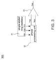
- FIG. 3 is a schematic diagram showing a single-ended oscillation device for generating a fully differential signal according to an embodiment of the invention.
- FIG. 4A is a schematic diagram showing a single-ended oscillation device for generating a fully differential signal according to another embodiment of the invention.
- FIG. 4B is a wave diagram of the single-ended oscillation device for generating a fully differential signal of FIG. 4A .
- FIG. 4C is a schematic diagram showing a single-ended oscillation device for generating a fully differential signal according to another embodiment of the invention.
- FIG. 5 is a flow chart showing a method of generating a fully differential signal by using a single-ended oscillation device according to an embodiment of the invention.
- FIG. 3 is a schematic diagram showing a single-ended oscillation device 300 for generating a fully differential signal according to an embodiment of the invention.
- the single-ended oscillation device 300 includes a single-ended ring oscillator 31 , a phase processing unit 32 and an amplifier 33 .
- the single-ended ring oscillator 31 includes an odd number (e.g., more than three) of inverting delay units (not shown).
- the inverting delay units delay an input signal and sequentially generate a first signal Ph 1 , a second signal Ph 2 , and a third signal Ph 3 .
- the second signal Ph 2 has a phase opposite to those of the first signal Ph 1 and the third signal Ph 3 .
- the phase processing unit 32 calculates (e.g., add or interpolate) the first signal Ph 1 and the third signal Ph 3 to generate an intermediate signal Phm.
- the intermediate signal Phm and the second signal Ph 2 are substantially opposite to each other in phase, i.e., substantially having a phase difference of 180 degrees. Signals with a phase difference of 180 degrees are fully differential signals.
- the phase processing unit 32 outputs the intermediate signal Phm and a delayed version of the second signal Ph 2 as the fully differential signal Vop and Von.
- the amplifier 33 amplifies the fully differential signal Vop and Von to generate a full swing signal with a duty cycle of 50%.
- the single-ended oscillation device 300 of the invention uses the phase processing unit 32 for generating the fully differentially signals and uses the amplifier 33 for amplifying the fully differentially signals to generate the full swing signals.
- the single-ended oscillation device 300 of the invention generates the fully differentially signals, thereby achieving the goal of reducing the circuit cost and the power consumption.
- FIG. 4A is a schematic diagram showing a single-ended oscillation device 400 for generating a fully differential signal according to an embodiment of the invention.
- the single-ended oscillation device 400 includes a single-ended ring oscillator 41 , a phase processing unit 42 and an amplifier 43 .
- the single-ended ring oscillator 41 includes an odd number of inverting delay units, e.g., 41 a - 41 e, as shown in FIG. 4A .
- each of odd-numbered inverting delay units generates an odd number signal while each even-numbered inverting delay unit delays the odd number signal of its previous-stage odd-numbered inverting delay unit to generate an even number signal.
- a first odd-numbered inverting delay unit 41 a generates a first odd number signal Pho 1 .
- a first even-numbered inverting delay unit 41 b delays the first odd number signal Pho 1 to generate a first even number signal Phe 1 .
- a second odd-numbered inverting delay unit 41 c delays the first even number signal Phe 1 to generate a second odd number signal Pho 2 .
- the phase processing unit 42 delays each odd number signal Pho and calculates (e.g., add or interpolate) two adjacent odd number signals, e.g., Pho 1 and Pho 2 , to generate an intermediate signal Phm. Besides, the phase processing unit 42 delays an even number signal, e.g., Phe 1 , between the two adjacent odd number signals Pho 1 and Pho 2 and causes the delayed signal ph 2 to be substantially aligned with the intermediate signal Phm.
- the intermediate signal Phm and the delayed signal Ph 2 are opposite to each other in phase, i.e., substantially having a phase difference of 180 degrees.
- the phase processing unit 42 includes a phase calculation unit 42 a and a phase delay unit 42 b.
- the phase calculation unit 42 a includes a first inverting delay unit 42 a 1 and a second inverting delay unit 42 a 2 .
- the first odd-numbered inverting delay unit 41 a delays an input signal by a predetermined period 1td to generate a first odd number signal pho 1 ; the first even-numbered inverting delay unit 41 b delays the first odd number signal pho 1 by a predetermined period 1td to generate a first even number signal phe 1 . In other words, the first even number signal phe 1 lags behind the input signal by 2td.
- the second odd-numbered inverting delay unit 41 c delays the first even number signal phe 1 by a predetermined period 1td to generate a second odd number signal pho 2 . In other words, the second odd number signal pho 2 lags behind the input signal by 3td.
- the phase calculation unit 42 a performs calculation (addition or interpolation) on the first odd number signal pho 1 and the second odd number signal pho 2 to generate an intermediate signal Phm that substantially lags behind the input signal by 2td.
- the delayed signal ph 2 and the intermediate signal Phm are substantially aligned and opposite to each other in phase by 180 degrees, so the intermediate signal Phm and the delayed signal Ph 2 are used as the fully differential signals Vop and Von.
- first odd number signal Pho 1 , the second odd number signal Pho 2 and the first even number signal phe 1 have been respectively inverted and delayed by the inverting delay unit 42 a 1 and 42 a 2 and the phase delay unit 42 b as shown in FIG. 4A , the first odd number signal Pho 1 , the second odd number signal Pho 2 and the first even number signal phe 1 still maintain their corresponding opposite relationships and delay period (s) as shown in FIG. 4B .
- the size(width ⁇ length) of the phase processing unit 42 including the inverting delay unit 42 a 1 and 42 a 2 and the phase delay unit 42 b is less than that of the single-ended ring oscillator 41 including the inverting delay units 41 a - 41 e, thereby reducing the manufacturing cost in practice.
- the gate width to length ratios (W/L) of the delay units 42 a 1 , 42 a 2 and 42 b are less than those of the inverting delay units 41 a - 41 e, thus reducing the power consumption.
- a driving capability ratio of the delay units 42 a 1 , 42 a 2 and 42 b can be 1:1:2, causing the capabilities of driving the fully differential signals Vop and Von to be substantially equal.
- a loading ratio of the delay units 42 a 1 , 42 a 2 and 42 b can be 1:1:1, causing the delay period of the intermediate signal Phm to be close to the average delay period of the first odd number signal Pho 1 and the second odd number signal Pho 2 ; besides, the intermediate signal Phm and the delayed signal Ph 2 are substantially aligned and opposite in phase by 180 degrees.
- the invention can meet the circuit design needs by adjusting the gate width to length ratios (W/L) and the product (W*L) of the delay units 42 a 1 , 42 a and 42 b.
- the amplifier 43 amplifies the fully differential signal Vop and Von to generate a full swing signal with a duty cycle of 50%.
- the single-ended oscillation device 400 of the invention can generate the full swing signal, capable of achieving the goal of reducing the circuit cost and the power consumption.
- two buffers 42 C 1 and 42 C 2 are added between the phase processing unit 42 and the amplifier 43 for signal buffering protection.
- phase operations are performed on three adjacent output signals from the odd number of inverting delay units to produce the fully differential signal including two signals opposite to each other in phase.
- any one of the even-numbered inverting delay units between the output signal of the first odd-numbered inverting delay unit and the output signal of the Nth odd-numbered inverting delay unit can be selected as one of the differential signal; besides, calculations are performed on the output signals of the first odd-numbered inverting delay unit and the N th odd-numbered inverting delay unit to obtain the other of the differential signal.
- FIG. 5 is a flow chart showing a method of generating a fully differential signal by using a single-ended oscillation device according to an embodiment of the invention.
- the method of generating a fully differential signal by using a single-ended oscillation device is described with reference to FIG. 5 .
- Step S 502 Start.
- Step S 504 Generate a first signal, a second signal and a third signal by using a single-ended ring oscillator including an odd number of inverting delay units.
- the first signal, the second signal and the third signal are oscillation signals.
- Step S 506 Generate an intermediate signal according to the first signal and the third signal.
- the intermediate signal and the second signal have a phase difference of 180 degrees.
- Step S 508 Generate a fully differential signal according to the intermediate signal and the second signal.
- Step S 510 End.
Landscapes
- Manipulation Of Pulses (AREA)
- Stabilization Of Oscillater, Synchronisation, Frequency Synthesizers (AREA)
- Pulse Circuits (AREA)
- Amplifiers (AREA)
Abstract
Description
Claims (13)
Applications Claiming Priority (3)
| Application Number | Priority Date | Filing Date | Title |
|---|---|---|---|
| TW102102907U | 2013-01-25 | ||
| TW102102907A TWI517559B (en) | 2013-01-25 | 2013-01-25 | Single-ended ring oscillator with fully differential signal and method thereof |
| TW102102907 | 2013-01-25 |
Publications (2)
| Publication Number | Publication Date |
|---|---|
| US20140210562A1 US20140210562A1 (en) | 2014-07-31 |
| US9048822B2 true US9048822B2 (en) | 2015-06-02 |
Family
ID=51222258
Family Applications (1)
| Application Number | Title | Priority Date | Filing Date |
|---|---|---|---|
| US14/158,034 Active US9048822B2 (en) | 2013-01-25 | 2014-01-17 | Single ended ring oscillator with fully differential signal |
Country Status (3)
| Country | Link |
|---|---|
| US (1) | US9048822B2 (en) |
| CN (1) | CN103973301B (en) |
| TW (1) | TWI517559B (en) |
Families Citing this family (1)
| Publication number | Priority date | Publication date | Assignee | Title |
|---|---|---|---|---|
| US9209821B2 (en) * | 2014-01-24 | 2015-12-08 | Intel Corporation | Apparatus for generating quadrature clock phases from a single-ended odd-stage ring oscillator |
Citations (2)
| Publication number | Priority date | Publication date | Assignee | Title |
|---|---|---|---|---|
| US20070018737A1 (en) * | 2005-07-19 | 2007-01-25 | Drake Alan J | High frequency ring oscillator with feed-forward paths |
| US20070241826A1 (en) * | 2006-03-31 | 2007-10-18 | Sony Corporation | Oscillating circuit |
Family Cites Families (4)
| Publication number | Priority date | Publication date | Assignee | Title |
|---|---|---|---|---|
| US6989697B2 (en) * | 2004-01-15 | 2006-01-24 | Organicid, Inc. | Non-quasistatic phase lock loop frequency divider circuit |
| US7852161B2 (en) * | 2009-01-14 | 2010-12-14 | Advanced Micro Devices, Inc. | Complementary ring oscillator with capacitive coupling |
| US20100201451A1 (en) * | 2009-02-06 | 2010-08-12 | Stephen Wu | Method and system for frequency calibration of a voltage controlled ring oscillator |
| US8265568B2 (en) * | 2009-03-19 | 2012-09-11 | Qualcomm Incorporated | Frequency divider with synchronized outputs |
-
2013
- 2013-01-25 TW TW102102907A patent/TWI517559B/en active
- 2013-08-16 CN CN201310359746.7A patent/CN103973301B/en active Active
-
2014
- 2014-01-17 US US14/158,034 patent/US9048822B2/en active Active
Patent Citations (2)
| Publication number | Priority date | Publication date | Assignee | Title |
|---|---|---|---|---|
| US20070018737A1 (en) * | 2005-07-19 | 2007-01-25 | Drake Alan J | High frequency ring oscillator with feed-forward paths |
| US20070241826A1 (en) * | 2006-03-31 | 2007-10-18 | Sony Corporation | Oscillating circuit |
Also Published As
| Publication number | Publication date |
|---|---|
| TW201431281A (en) | 2014-08-01 |
| TWI517559B (en) | 2016-01-11 |
| CN103973301A (en) | 2014-08-06 |
| US20140210562A1 (en) | 2014-07-31 |
| CN103973301B (en) | 2017-03-29 |
Similar Documents
| Publication | Publication Date | Title |
|---|---|---|
| US9571106B2 (en) | Delay locked loop circuit | |
| US7863957B2 (en) | Duty cycle correction circuit and semiconductor integrated circuit apparatus including the same | |
| US8149034B2 (en) | Delay lines, methods for delaying a signal, and delay lock loops | |
| US6680635B2 (en) | Apparatus and method for generating output clock signal having controlled timing | |
| JP2005135567A (en) | Delay locked loop and clock generation method therefor | |
| US7282978B2 (en) | Duty cycle correction device | |
| KR101125018B1 (en) | Digital Delay cell and Delay line circuit having the same | |
| CN107046416A (en) | Duty-cycle correction circuit | |
| US7932766B2 (en) | Digitally controlled oscillator with the wide operation range | |
| US9018990B2 (en) | Duty cycle tuning circuit and method thereof | |
| US7528668B2 (en) | Differential amplifier, differential amplifying method, and phase locked loop and delay locked loop using the same | |
| US7884661B2 (en) | Clock generator circuit, method of clock generating, and data output circuit using the clock generating circuit and method | |
| US9048822B2 (en) | Single ended ring oscillator with fully differential signal | |
| US9716505B2 (en) | System and method for enhanced clocking operation | |
| US10707849B2 (en) | Synchronous mirror delay circuit and synchronous mirror delay operation method | |
| US8971447B1 (en) | Variable delay of data signals | |
| US8487682B2 (en) | Multi-phase clock generator | |
| US10367487B1 (en) | Quadrature clock divider with 25%/75% duty cycle | |
| KR100782481B1 (en) | Clock signal driver and clock signal providing circuit having same | |
| US8803567B2 (en) | Frequency multiplier system and method of multiplying frequency | |
| JP3498891B2 (en) | Clock synchronization delay control circuit | |
| US11169561B2 (en) | Clock data recovery device and method to alternatively adjust phases of outputted clock signals | |
| US7492199B2 (en) | Fully synchronous DLL with architected update window | |
| JP2006333150A (en) | Integrated circuit device | |
| JP5347749B2 (en) | Differential receiver circuit |
Legal Events
| Date | Code | Title | Description |
|---|---|---|---|
| AS | Assignment |
Owner name: REALTEK SEMICONDUCTORS CORP., TAIWAN Free format text: ASSIGNMENT OF ASSIGNORS INTEREST;ASSIGNOR:TU, CHUAN PING;REEL/FRAME:032038/0946 Effective date: 20140112 |
|
| AS | Assignment |
Owner name: REALTEK SEMICONDUCTOR CORP., TAIWAN Free format text: CORRECTIVE ASSIGNMENT TO CORRECT THE ASSIGNEE'S NAME PREVIOUSLY RECORDED AT REEL: 032038 FRAME: 0946. ASSIGNOR(S) HEREBY CONFIRMS THE ASSIGNMENT;ASSIGNOR:TU, CHUAN PING;REEL/FRAME:035487/0140 Effective date: 20140112 |
|
| STCF | Information on status: patent grant |
Free format text: PATENTED CASE |
|
| MAFP | Maintenance fee payment |
Free format text: PAYMENT OF MAINTENANCE FEE, 4TH YEAR, LARGE ENTITY (ORIGINAL EVENT CODE: M1551) Year of fee payment: 4 |
|
| MAFP | Maintenance fee payment |
Free format text: PAYMENT OF MAINTENANCE FEE, 8TH YEAR, LARGE ENTITY (ORIGINAL EVENT CODE: M1552); ENTITY STATUS OF PATENT OWNER: LARGE ENTITY Year of fee payment: 8 |