US9024178B2 - Solar cell element - Google Patents
Solar cell element Download PDFInfo
- Publication number
- US9024178B2 US9024178B2 US14/143,294 US201314143294A US9024178B2 US 9024178 B2 US9024178 B2 US 9024178B2 US 201314143294 A US201314143294 A US 201314143294A US 9024178 B2 US9024178 B2 US 9024178B2
- Authority
- US
- United States
- Prior art keywords
- layer
- zno
- type semiconductor
- less
- columnar crystal
- Prior art date
- Legal status (The legal status is an assumption and is not a legal conclusion. Google has not performed a legal analysis and makes no representation as to the accuracy of the status listed.)
- Expired - Fee Related
Links
Images


Classifications
-
- H01L31/02167—
-
- H—ELECTRICITY
- H10—SEMICONDUCTOR DEVICES; ELECTRIC SOLID-STATE DEVICES NOT OTHERWISE PROVIDED FOR
- H10F—INORGANIC SEMICONDUCTOR DEVICES SENSITIVE TO INFRARED RADIATION, LIGHT, ELECTROMAGNETIC RADIATION OF SHORTER WAVELENGTH OR CORPUSCULAR RADIATION
- H10F77/00—Constructional details of devices covered by this subclass
- H10F77/30—Coatings
- H10F77/306—Coatings for devices having potential barriers
- H10F77/311—Coatings for devices having potential barriers for photovoltaic cells
-
- H01L31/022483—
-
- H01L31/0392—
-
- H01L31/03921—
-
- H01L31/1884—
-
- H—ELECTRICITY
- H10—SEMICONDUCTOR DEVICES; ELECTRIC SOLID-STATE DEVICES NOT OTHERWISE PROVIDED FOR
- H10F—INORGANIC SEMICONDUCTOR DEVICES SENSITIVE TO INFRARED RADIATION, LIGHT, ELECTROMAGNETIC RADIATION OF SHORTER WAVELENGTH OR CORPUSCULAR RADIATION
- H10F71/00—Manufacture or treatment of devices covered by this subclass
- H10F71/138—Manufacture of transparent electrodes, e.g. transparent conductive oxides [TCO] or indium tin oxide [ITO] electrodes
-
- H—ELECTRICITY
- H10—SEMICONDUCTOR DEVICES; ELECTRIC SOLID-STATE DEVICES NOT OTHERWISE PROVIDED FOR
- H10F—INORGANIC SEMICONDUCTOR DEVICES SENSITIVE TO INFRARED RADIATION, LIGHT, ELECTROMAGNETIC RADIATION OF SHORTER WAVELENGTH OR CORPUSCULAR RADIATION
- H10F77/00—Constructional details of devices covered by this subclass
- H10F77/10—Semiconductor bodies
- H10F77/16—Material structures, e.g. crystalline structures, film structures or crystal plane orientations
- H10F77/169—Thin semiconductor films on metallic or insulating substrates
- H10F77/1692—Thin semiconductor films on metallic or insulating substrates the films including only Group IV materials
-
- H—ELECTRICITY
- H10—SEMICONDUCTOR DEVICES; ELECTRIC SOLID-STATE DEVICES NOT OTHERWISE PROVIDED FOR
- H10F—INORGANIC SEMICONDUCTOR DEVICES SENSITIVE TO INFRARED RADIATION, LIGHT, ELECTROMAGNETIC RADIATION OF SHORTER WAVELENGTH OR CORPUSCULAR RADIATION
- H10F77/00—Constructional details of devices covered by this subclass
- H10F77/20—Electrodes
- H10F77/244—Electrodes made of transparent conductive layers, e.g. transparent conductive oxide [TCO] layers
- H10F77/251—Electrodes made of transparent conductive layers, e.g. transparent conductive oxide [TCO] layers comprising zinc oxide [ZnO]
-
- Y—GENERAL TAGGING OF NEW TECHNOLOGICAL DEVELOPMENTS; GENERAL TAGGING OF CROSS-SECTIONAL TECHNOLOGIES SPANNING OVER SEVERAL SECTIONS OF THE IPC; TECHNICAL SUBJECTS COVERED BY FORMER USPC CROSS-REFERENCE ART COLLECTIONS [XRACs] AND DIGESTS
- Y02—TECHNOLOGIES OR APPLICATIONS FOR MITIGATION OR ADAPTATION AGAINST CLIMATE CHANGE
- Y02E—REDUCTION OF GREENHOUSE GAS [GHG] EMISSIONS, RELATED TO ENERGY GENERATION, TRANSMISSION OR DISTRIBUTION
- Y02E10/00—Energy generation through renewable energy sources
- Y02E10/50—Photovoltaic [PV] energy
Definitions
- the present disclosure relates to a solar cell element.
- FIG. 14 shows a solar cell element disclosed in Patent Literature 1 (Japanese Patent laid-open Publication No. H11-220154).
- This solar cell element comprises a substrate 101 , a reverse surface reflective layer 102 , a first transparent electrode layer 103 a formed of ZnO, a second transparent electrode layer 103 b formed from ZnO, a semiconductor layer 105 , an upper part transparent electrode 106 , and a collective electrode in this order.
- the second clear electrode layer 103 b is composed of a plurality of columnar crystal grains. Each columnar crystal grain has a longitudinal direction along a normal line direction of the substrate 101 .
- the second clear electrode layer 103 b has a region where a plurality of columnar crystal grains radiate upwardly.
- the upper transparent electrode 106 is irradiated with light from above to generate a voltage difference between the first clear electrode layer 103 and the upper transparent electrode 106 .
- One non-limiting and exemplary embodiments provides a novel solar cell element having high photoelectric conversion efficiency.
- the techniques disclosed here feature: a method for generating an electric power using a solar cell element, the method comprising:
- the transparent substrate body, the Li x Ag 1-x layer, the ZnO layer, the transparent conductive layer, and the photoelectric conversion layer are stacked in this order;
- the n-side electrode is electrically connected to the n-type semiconductor layer
- the p-side electrode is electrically connected to the p-type semiconductor layer
- x represents a value of not less than 0.001 and not more than 0.05
- the Li x Ag 1-x layer has a thickness of not less than 2 nanometers and not more than 15 nanometers;
- the ZnO layer has a arithmetical mean roughness of not less than 20 nanometers and not less than 760 nanometers;
- the ZnO layer is composed of a plurality of ZnO columnar crystal grains grown on the surface of the Li x Ag 1-x layer;
- each ZnO columnar crystal grain has a longitudinal direction along a normal line direction of the transparent substrate body
- each ZnO columnar crystal grain has a width which increases from the Li x Ag 1-x layer toward the transparent conductive layer;
- each ZnO columnar crystal grain appears by cutting each ZnO columnar crystal grain along the normal line direction of the transparent substrate body;
- each ZnO columnar crystal grain has a R2/R1 ratio of not less than 1.1 and not more than 1.6;
- R1 represents the width of one end of the ZnO columnar crystal grain, the one end being in contact with the surface of the Li x Ag 1-x layer;
- R2 represents the width of the other end of the ZnO columnar crystal grain
- One non-limiting and exemplary embodiments provides a novel solar cell element having high photoelectric conversion efficiency.
- FIG. 1 shows a cross-sectional view of the solar cell element 9 according to the embodiment
- FIG. 2 shows a cross-sectional view of one step included in a method for fabricating the solar cell element 9 ;
- FIG. 3 shows a cross-sectional view of one step included in a method for fabricating the solar cell element 9 , subsequently to FIG. 2 ;
- FIG. 4 shows a cross-sectional view of one step included in a method for fabricating the solar cell element 9 , subsequently to FIG. 3 ;
- FIG. 5 shows a cross-sectional view of one step included in a method for fabricating the solar cell element 9 , subsequently to FIG. 4 ;
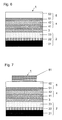
- FIG. 6 shows a cross-sectional view of one step included in a method for fabricating the solar cell element 9 , subsequently to FIG. 5 ;
- FIG. 7 shows a cross-sectional view of one step included in a method for fabricating the solar cell element 9 , subsequently to FIG. 6 ;
- FIG. 8 shows a cross-sectional view of one step included in a method for fabricating the solar cell element 9 , subsequently to FIG. 7 ;
- FIG. 9 shows a cross-sectional view of one step included in a method for fabricating the solar cell element 9 , subsequently to FIG. 8 ;
- FIG. 10 shows a cross-sectional view of one step included in a method for fabricating the solar cell element 9 , subsequently to FIG. 9 ;
- FIG. 11 shows a cross-sectional view of one step included in a method for fabricating the solar cell element 9 , subsequently to FIG. 10 ;
- FIG. 12 shows one example of a surface roughness profile
- FIG. 13 shows an I-V-curve obtained in the example 1
- FIG. 14 shows a solar cell element disclosed in Patent Literature 1 (Japanese Patent laid-open Publication No. H11-220154);
- FIG. 15 shows a drawing for explaining Ra
- FIG. 16 shows an enlarged view of the part surrounded by a dash line A depicted in FIG. 1 ;
- FIG. 17 shows an SEM image of the Li x Ag 1-x layer 22 according to the example 1.
- a method for generating an electric power using a solar cell element including:
- the transparent substrate body, the Li x Ag 1-x layer, the ZnO layer, the transparent conductive layer, and the photoelectric conversion layer are stacked in this order;
- the n-side electrode is electrically connected to the n-type semiconductor layer
- the p-side electrode is electrically connected to the p-type semiconductor layer
- x represents a value of not less than 0.001 and not more than 0.05
- the Li x Ag 1-x layer has a thickness of not less than 2 nanometers and not more than 15 nanometers;
- the ZnO layer has a arithmetical mean roughness of not less than 20 nanometers and not less than 760 nanometers;
- the ZnO layer is composed of a plurality of ZnO columnar crystal grains grown on the surface of the Li x Ag 1-x layer;
- each ZnO columnar crystal grain has a longitudinal direction along a normal line direction of the transparent substrate body
- each ZnO columnar crystal grain has a width which increases from the Li x Ag 1-x layer toward the transparent conductive layer;
- each ZnO columnar crystal grain appears by cutting each ZnO columnar crystal grain along the normal line direction of the transparent substrate body;
- each ZnO columnar crystal grain has a R2/R1 ratio of not less than 1.1 and not more than 1.6;
- R1 represents the width of one end of the ZnO columnar crystal grain, the one end being in contact with the surface of the Li x Ag 1-x layer;
- R2 represents the width of the other end of the ZnO columnar crystal grain
- the solar cell element 9 further may include a reverse surface electrode layer
- the photoelectric conversion layer may be interposed between the n-type semiconductor layer and the reverse surface electrode layer.
- n-type semiconductor layer 41 may be interposed between the transparent conductive layer and the p-type semiconductor layer;
- n-side electrode may be formed on the transparent conductive layer
- the p-side electrode may be formed on the reverse surface electrode layer.
- the ZnO layer may have a volume resistivity of not less than 1 ⁇ 10 ⁇ 3 ⁇ cm.
- the transparent conductive layer may have a volume resistivity of less than 1 ⁇ 10 ⁇ 3 ⁇ cm.
- the ZnO layer may have a volume resistivity of not less than 1 ⁇ 10 ⁇ 3 ⁇ cm
- a solar cell element including:
- a photoelectric conversion layer including an n-type semiconductor layer and a p-type semiconductor layer
- the transparent substrate body, the Li x Ag 1-x layer, the ZnO layer, the transparent conductive layer, and the photoelectric conversion layer are stacked in this order;
- the n-side electrode is electrically connected to the n-type semiconductor layer
- the p-side electrode is electrically connected to the p-type semiconductor layer
- x represents a value of not less than 0.001 and not more than 0.05
- the Li x Ag 1-x layer has a thickness of not less than 2 nanometers and not more than 15 nanometers;
- the ZnO layer has a arithmetical mean roughness of not less than 20 nanometers and not less than 760 nanometers;
- the ZnO layer is composed of a plurality of ZnO columnar crystal grains grown on the surface of the Li x Ag 1-x layer;
- each ZnO columnar crystal grain has a longitudinal direction along a normal line direction of the transparent substrate body
- each ZnO columnar crystal grain has a width which increases from the Li x Ag 1-x layer toward the transparent conductive layer;
- each ZnO columnar crystal grain appears by cutting each ZnO columnar crystal grain along the normal line direction of the transparent substrate body;
- each ZnO columnar crystal grain has a R2/R1 ratio of not less than 1.1 and not more than 1.6;
- R1 represents the width of one end of the ZnO columnar crystal grain, the one end being in contact with the surface of the Li x Ag 1-x layer;
- R2 represents the width of the other end of the ZnO columnar crystal grain.
- the solar cell element further comprises a reverse surface electrode layer
- the photoelectric conversion layer is interposed between the n-type semiconductor layer and the reverse surface electrode layer.
- n-type semiconductor layer may be interposed between the transparent conductive layer and the p-type semiconductor layer
- the p-type semiconductor layer may be interposed between the n-type semiconductor layer and the reverse surface electrode layer.
- n-side electrode may be formed on the transparent conductive layer
- the p-side electrode may be formed on the reverse surface electrode layer.
- the ZnO layer may have a volume resistivity of not less than 1 ⁇ 10 ⁇ 3 ⁇ cm.
- the transparent conductive layer may have a volume resistivity of less than 1 ⁇ 10 ⁇ 3 ⁇ cm.
- the ZnO layer may have a volume resistivity of not less than 1 ⁇ 10 ⁇ 3 ⁇ cm
- the transparent conductive layer may be formed of ZnO having a volume resistivity of less than 1 ⁇ 10 ⁇ 3 ⁇ cm.
- a solar cell element 9 is prepared.
- FIG. 1 shows a cross-sectional view of the solar cell element 9 according to the embodiment.
- the solar cell element 9 comprises a transparent substrate 2 , a transparent conductive layer 3 , a photoelectric conversion layer 4 , a reverse surface electrode layer 5 , an n-side electrode 6 , and a p-side electrode 7 in this order.
- the transparent substrate 2 includes a transparent substrate body 21 , Li x Ag 1-x layer 22 , and a ZnO layer 23 .
- the Li x Ag 1-x layer 22 is interposed between the transparent substrate body 21 and the ZnO layer 23 .
- the transparent substrate body 21 is permeable to light (e.g., sunlight) having a wavelength of not less than 300 nanometers and not more than 1,100 nanometers.
- An example of the transparent substrate body 21 is a glass substrate, a ceramics substrate, a plastic substrate, or a metal substrate.
- a glass substrate having a thickness of 0.3 millimeters-7 millimeters is desirable.
- the Li x Ag 1-x layer 22 consists of alloy of sodium and silver.
- the character of “x” represents a value of not less than 0.001 and not more than 0.05. When the value of x is less than 0.001, photoelectric conversion efficiency is decreased. See the comparative example 3. Similarly, when the value of x is more than 0.05, the photoelectric conversion efficiency is decreased. See the comparative example 4.
- the Li x Ag 1-x layer 22 has a thickness of not less than 2 nanometers and not more than 15 nanometers. Since the Li x Ag 1-x layer 22 is significantly thin, the Li x Ag 1-x layer 22 is permeable to light. When the Li x Ag 1-x layer 22 is not provided, the photoelectric conversion efficiency is decreased. When the Li x Ag 1-x layer 22 has a thickness of more than 15 nanometers, the photoelectric conversion efficiency is decreased.
- the Li x Ag 1-x layer 22 may be formed by a sputtering method.
- the ZnO layer 23 is an arithmetical mean deviation of the profile (hereinafter, referred to as “Ra”) of not less than 20 nanometers and not more than 760 nanometers.
- the arithmetical mean deviation of the profile Ra is the arithmetic mean of the absolute values of distances from the mean line to the surface roughness profile.
- Ra (1/ L ) ⁇ 0 L
- L Evaluation length
- f(x) Surface roughness profile
- FIG. 15 shows a drawing for explaining Ra.
- the value of Ra may be measured with a surface roughness measuring apparatus.
- the surface roughness measuring apparatus is available from Taylor Hobson company, as trade name “CCI Lite”.
- the surface roughness profile is a profile obtained by measuring the projection-and-recess shape of the surface of the object using a surface roughness measuring apparatus.
- FIG. 12 shows an example of the surface roughness profile.
- ZnO is transparent. Therefore, the ZnO layer 23 is permeable to light.
- the ZnO layer 23 is composed of a plurality of ZnO columnar crystal grains 23 a .
- Each ZnO columnar crystal grain 23 a is grown, using Ag contained in the Li x Ag 1-x layer 22 as a core. Li contained in the Li x Ag 1-x layer 22 improves the crystallinity of the ZnO columnar crystal grain 23 a.
- Each ZnO columnar crystal grain 23 a has a longitudinal direction along a normal line direction of the transparent substrate body 21 .
- Each ZnO columnar crystal grain 23 a has a width which increases from the Li x Ag 1-x layer 22 toward the transparent electrode layer 3 . More particularly, Each ZnO columnar crystal grain 23 a has a R2/R1 ratio of not less than 1.1 and not more than 1.6. As shown in FIG. 16 , the value of R1 represents a width of an end of the ZnO columnar crystal grain 23 a which is in contact with the Li x Ag 1-x layer 22 which is in contact with the ZnO layer 3 . The value of R2 represents a width of the other end of the ZnO columnar crystal grain 23 a . When the R2/R1 ratio is less than 1.1, the photoelectric conversion efficiency is decreased. See the comparative example 1. When the R2/R1 is more than 1.6, the photoelectric conversion efficiency is decreased. See the comparative example 2.
- the width of the ZnO columnar crystal grain 23 a appears by cutting the ZnO columnar crystal grain 23 a along a normal line direction of the transparent substrate body 21 . This width is substantially perpendicular to the longitudinal direction of the ZnO columnar crystal grain 23 a.
- the ZnO layer 23 has a volume resistivity of more than 1 ⁇ 10 ⁇ 3 ⁇ cm.
- the transparent conductive layer 3 is interposed between the ZnO layer 23 and the photoelectric conversion layer 4 .
- An example of the material of the transparent conductive layer 3 is zinc oxide doped with at least one selected from the group consisting of gallium, aluminum and boron.
- the transparent conductive layer 3 has a volume resistivity of less than 1 ⁇ 10 ⁇ 3 ⁇ cm. Since the ZnO layer 23 has a great volume resistivity, it is difficult to obtain an electric power from the ZnO layer 23 efficiently. Therefore, it is desirable to provide such a low-resistance transparent conductive layer 3 .
- the photoelectric conversion layer 4 includes an n-type semiconductor layer 41 and a p-type semiconductor layer 42 .
- An example of the material of the n-type semiconductor layer 41 is silicon or GaAs.
- An example of the material of the p-type semiconductor layer 42 is also silicon or GaAs.
- the n-type semiconductor layer 41 and the p-type semiconductor layer 42 are formed in this order on the transparent conductive layer 3 .
- the n-type semiconductor layer 41 is in contact with the p-type semiconductor layer 42 to form a pn-junction.
- the solar cell element 9 may comprise the reverse surface electrode layer 5 .
- the reverse surface electrode layer 5 may include a buffer layer 51 and a reflective layer 52 .
- the buffer layer 51 is interposed between the photoelectric conversion layer 42 and the reflective layer 52 .
- An example of the material of the buffer layer 51 is (a) transparent conductive material such as zinc oxide, indium oxide, tin oxide, or cadmium oxide, or (b) transparent semiconductor material such as iron oxide, titanium oxide, zinc selenide, or zinc sulphide. Zinc oxide is desirable.
- An example of the material of the reflective layer 52 is gold, silver, copper, aluminum, platinum, or alloy thereof. Silver is desirable.
- the n-side electrode 6 is electrically connected to the n-type semiconductor layer 41 .
- the n-side electrode 6 forms an ohmic contact together with the transparent conductive layer 3 .
- An example of a suitable material of the n-side electrode 6 is silver, gold, copper, aluminum, platinum, or alloy thereof. Platinum is desirable.
- the p-side electrode 7 is electrically connected to the p-type semiconductor layer 42 .
- the p-side electrode 7 forms an ohmic contact together with the reflective layer 52 .
- An example of a suitable material of the p-side electrode 7 is silver, gold, copper, aluminum, platinum, or alloy thereof. Platinum is desirable.
- the transparent substrate body 21 is prepared.
- a glass substrate is desirable.
- the Li x Ag 1-x layer 22 is formed on the surface of transparent substrate body 21 by a conventional semiconductor growth method such as a RF magnetron sputtering method or a vacuum evaporation method.
- the Li x Ag 1-x layer 22 is heated.
- An example of a heating method is an anneal method, a vacuum heating method, a UV-ozone method, an advanced oxidation process method, an anneal method under oxygen atmosphere, or an anode oxidation method.
- An anneal method under a temperature of 50-800 degrees Celsius is desirable.
- the width of the Li x Ag 1-x layer 22 is decreased by the heat treatment. In other words, the area of the Li x Ag 1-x layer 22 is decreased. In this way, island-shaped Li x Ag 1-x areas 22 are formed on the transparent substrate body 21 .
- the Li x Ag 1-x layer 22 may not cover the whole surface of the transparent substrate body 21 .
- a portion 21 b of the transparent substrate body 21 which is not covered may be exposed.
- FIG. 16 shows an enlarged view of the part surrounded by the dashed line A depicted in FIG. 1 .
- the ZnO layer 23 is composed of the plurality of the ZnO columnar crystal grains 23 a . Since each ZnO columnar crystal grain 23 a has the R2/R1 ratio of not less than 1.1 and not more than 1.6, the upper surface of the ZnO layer 23 does not have an interspace.
- the portion 21 b of the transparent substrate body 21 which is covered neither by the Li x Ag 1-x layer 22 nor by the ZnO layer 23 may be exposed.
- the surface roughness of the Li x Ag 1-x layer 22 may be varied by the temperature of the heat treatment.
- the ZnO layer 23 is formed on the Li x Ag 1-x layer 22 by a CBD method using a mixture of Zn (NO 3 ) 2 and hexamethylene tetramine (hereinafter, referred to as “HMT”) under a temperature of 20-90 degrees Celsius.
- CBD hexamethylene tetramine
- the surface projection-and-recess roughness of the formed ZnO layer 23 become larger with increase of the time of the processing time of the reactive ion etching or the chemical etching.
- CH 4 gas may be used.
- chloride solution may be used.
- the ZnO layer 23 is in contact with the Li x Ag 1-x layer 22 . To be more exact, the ZnO layer 23 is in contact with the top surface of the Li x Ag 1-x layer 22 .
- the transparent conductive layer 3 is formed on the ZnO layer 23 uniformly.
- An example of the method for forming the transparent conductive layer 3 is a pulse laser deposition method (hereinafter, referred to as “PLD method”).
- the n-type silicon layer 41 and the p-type silicon layer 42 are deposited on the transparent electrically conducting layer 3 by a plasma CVD method to form the photoelectric conversion layer 4 .
- the n-type silicon layer 41 may be formed by a plasma CVD method using a gaseous mixture containing phosphine, silane, and hydrogen.
- the p-type silicon layer 41 is deposited by a plasma CVD method using a gaseous mixture containing diborane, silane, methane, and hydrogen.
- the reverse surface electrode layer 5 including a buffer layer 51 and a reflective layer 52 is formed.
- An example of a method for forming the buffer layer 51 is a PLD method, a RF magnetron sputtering method, or a vacuum evaporation method.
- An example of a method for forming the reflective layer 52 is a RF magnetron sputtering method or a vacuum evaporation method.
- a first mask 81 is formed on the surface of the laminate 1 by photolithography.
- an unnecessary portion of the laminate 1 is removed by etching. More particularly, an unnecessary portion of the reflective layer 52 and an unnecessary portion of the buffer layer 51 are removed by wet-etching using with a mixture of hydrochloric acid and nitric acid. Furthermore, an unnecessary portion of the photoelectric conversion layer 4 is removed by ICP plasma etching using a gaseous mixture of oxygen, Ar, and mixed gas of SF 6 , using this resist film as the first mask 81 .
- a second mask 82 is formed by photolithography.
- This second mask 82 has a first opening 821 and a second opening 822 .
- the transparent conductive layer 3 is located under the first opening 821 .
- the reflective layer 52 is located under the second opening 822 .
- a metal layer is formed on the second mask 82 by a sputter vacuum deposition method or an electron beam evaporation method. Finally, the second mask 82 is removed, as shown in FIG. 11 . In this way, the n-side electrode 6 and the p-side electrode 7 are formed.
- the transparent substrate body 21 is irradiated with light.
- the light penetrates the transparent substrate body 21 , the Li x Ag 1-x layer 22 , the ZnO layer 23 , and the transparent conductive layer 3 to reach the photoelectric conversion layer 4 .
- the light is converted into electricity by the photoelectric conversion layer 4 . In this way, an electric power is generated between the n-side electrode 6 and the p-side electrode 7 .
- the solar cell element 9 shown in FIG. 1 was fabricated in accordance with the method shown in FIG. 2-FIG . 11 .
- a glass substrate having a thickness of 5 millimeters was prepared as the transparent substrate body 21 .
- the transparent substrate body 21 had a length of 25 millimeters and a width of 25 millimeters.
- the transparent substrate body 21 had a light transmittance of 88-90%.
- the transparent substrate body 21 was immersed in ethanol and washed under an ultrasonic application.
- a RF magnetron sputtering method used was a mixture target of Li and Ag having a molar ratio of 1:999.
- the formed Li x Ag 1-x layer 22 had a thickness of 2 nanometers.
- the transparent substrate body 21 thus provided was heated under a temperature of 350 degrees Celsius for ten minutes.
- the transparent substrate body 21 was immersed in a liquid mixture of Zn (NO 3 ) 2 and HMT warmed at 70 degrees Celsius for three hours so as to form the ZnO layer 23 .
- the Zn (NO 3 ) 2 had a concentration of 0.1M.
- the HMT also had a concentration of 0.1M.
- the formed ZnO layer 23 had a thickness of 1 micrometer.
- the Ra of the formed ZnO layer 23 was measured with a surface roughness measuring apparatus (available from Taylor Hobson company, trade name “CCI Lite”). As a result, the value of Ra was 21 nanometers.
- FIG. 17 shows a SEM image of the ZnO layer 23 included in the laminate 1 which was thus cut. On the basis of the SEM image, the values of R1 and R2 were measured.
- the value of R1 was 117 nanometers.
- the value of R2 was 152 nanometers. Therefore, the R2/R1 ratio was approximately 1.3.
- volume resistivity RE ⁇ t ⁇ RCF
- the value of RE represents a resistance value measured according to a four-terminal measurement method.
- a measurement apparatus for measuring a resistance value measured according to the four-terminal measurement method is available from Mitsubishi Chemical Corporation, as a trade name: Loresta-Gp MCP-T610.
- the value of t represents a thickness of the ZnO layer 23 .
- RCF represents a resistivity correction factor.
- the value of RCF was 4.398.
- the ZnO layer 23 had a volume resistivity of 9.92 ⁇ 10 ⁇ 3 ⁇ cm.
- the transparent conductive layer 3 was formed on the ZnO layer 23 by a PLD method.
- the material of the transparent conductive layer 3 was zinc oxide where 5.7 weight % of gallium was doped.
- zinc oxide doped with gallium is referred to as “GZO”.
- the transparent conductive layer 3 had a thickness of 100 nanometers.
- the volume resistivity of the transparent conductive layer 3 was measured similarly to that of the ZnO layer 23 . As a result, the transparent conductive layer 3 had a volume resistivity of 5.2 ⁇ 10 ⁇ 4 ⁇ cm.
- the n-type semiconductor layer 41 consisting of n-type silicon and the p-type semiconductor layer 42 consisting of p-type silicon were formed in this order by a plasma CVD method so as to form the photoelectric conversion layer 4 .
- the n-type semiconductor layer 41 had a thickness of 40 nanometers.
- the p-type semiconductor layer 42 had a thickness of 11 nanometers.
- a GZO film having thickness of 40 nanometers was formed on the p-type semiconductor layer 42 by a sputter vacuum deposition method. In this way, the buffer layer 51 consisting of the GZO film was formed.
- a silver layer having a thickness of 200 nanometers was formed on the buffer layer 51 by a sputter vacuum deposition. In this way, the reflective layer 52 consisting of silver was formed.
- the resist film 81 of 20 millimeters square was formed on the reflective layer 52 by photolithography.
- this resist film as the first mask 81 , an unnecessary portion of the reflective layer 52 and an unnecessary portion of the buffer layer 51 were removed by wet-etching using liquid mixture of hydrochloric acid and nitric acid.
- an unnecessary portion of the photoelectric conversion layer 4 was removed by an ICP plasma etching using a gaseous mixture of oxygen, argon, and SF 6 .
- the first mask 81 was removed.
- the second mask 82 was formed by photolithography.
- the second mask 82 had a first opening 821 and a second opening 822 .
- the first opening 821 was formed on the transparent conductive layer 3 .
- the first opening 821 had a size of 22 millimeters square.
- the second opening 822 was formed on the reflective layer 52 .
- the second opening 822 had a size of 2 millimeters x 22 millimeters.
- a platinum film having a thickness of 100 nanometers was formed so that the second mask 82 was covered with the platinum film.
- the second mask 82 was removed to form the n-side electrode 6 consisting of platinum and the p-side electrode 7 consisting of platinum.
- the transparent substrate body 21 was irradiated with pseudo-sunlight, which is described later.
- the photoelectric conversion efficiency of the solar cell element 9 was calculated as below.
- the transparent substrate body 21 was irradiated with the pseudo-sunlight having power energy of 100 mW/cm 2 .
- the pseudo-sunlight was radiated from the lamp where a xenon lamp (available from Wacom Co., Ltd.) of 500 watts and a halogen lamp (available from Wacom Co., Ltd.) of 400 watts were combined together.
- a xenon lamp available from Wacom Co., Ltd.
- a halogen lamp available from Wacom Co., Ltd.
- the open circuit voltage Voc was measured when the n-side electrode 6 and the p-side electrode 7 were electrically opened.
- the short-circuit current Isc was measured when the n-side electrode 6 and the p-side electrode 7 were short-circuited.
- An I-V curve line as shown in FIG. 13 was obtained using a solar simulator (available from Wacom Co., Ltd., Trade name: Super Solar simulator WXS-90S-L2).
- FF fill factor
- the fill factor FF was calculated in accordance with the following math formula.
- Vmax means the voltage when the V max value of the I-V curve is maximum in FIG. 13 (See the arrow in FIG. 13 ).
- Imax means the electric current when the V ⁇ I value of the I-V curve is maximum in FIG. 13 (See the arrow in FIG. 13 ).
- Photoelectric conversion efficiency V oc ⁇ J sc ⁇ FF
- J sc I sc /S
- the experiment similar to the example 1 was conducted, except that ZnO nanoparticles having an average particle diameter (d50) of 2.2 nanometers were applied on the transparent substrate body 21 by a spin-coater method, instead of the Li x Ag 1-x layer 22 .
- the formed layer had a thickness of 2.2 nanometers.
- the ZnO nanoparticles were synthesized by a sol-gel method. The results are shown in Table 3.
- Example 1 Example 2
- Example 3 Example 4
- Example 5 Value of x 0.001 0.001 0.001 0.001 0.05 Thickness of 2.0 nm 15.0 nm 2.1 nm 2.1 nm 2.3 nm Li x Ag 1 ⁇ x layer 22 Zn(NO 3 ) 2 concentration 0.1M 0.1M 0.05M 0.75M 0.1M HMT concentration 0.1M 0.1M 0.05M 0.75M 0.1M R2 (unit: nanometer) 152 165 114 410 194 R1 (unit: nanometer) 117 127 104 256 129 R2/R1 ratio 1.3 1.4 1.1 1.6 1.5 Ra (unit: nanometer) 2.0 523 18 760 72 Photoelectric conversion 9.4% 9.8% 9.1% 8.9% 9.7% efficiency
- the Li x Ag 1-x layer 22 has a thickness of not less than 2 nanometers and not more than 15 nanometers. See the comparative example 6.
- the ZnO layer 23 had a value of Ra of not less than 20 and not more than 760 nanometers. See the comparative example 1 and comparative example 2.
- the present disclosure provides a solar cell element having high photoelectric conversion efficiency.
Landscapes
- Photovoltaic Devices (AREA)
- Life Sciences & Earth Sciences (AREA)
- Engineering & Computer Science (AREA)
- Sustainable Development (AREA)
- Sustainable Energy (AREA)
Abstract
Description
-
- a transparent substrate body;
- a LixAg1-x layer;
- a ZnO layer;
- a transparent conductive layer;
- a photoelectric conversion layer including an n-type semiconductor layer and a p-type semiconductor layer;
- an n-side electrode; and
- a p-side electrode;
-
- a transparent substrate body;
- a LixAg1-x layer;
- a ZnO layer;
- a transparent conductive layer;
- a photoelectric conversion layer including an n-type semiconductor layer and a p-type semiconductor layer;
- an n-side electrode; and
- a p-side electrode;
Ra=(1/L)·∫0 L |f(x)|dx (I)
Volume resistivity=RE·t·RCF
Photoelectric conversion efficiency=V oc ·J sc ·FF
Here, J sc =I sc /S
| TABLE 1 | ||||||
| Example 1 | Example 2 | Example 3 | Example 4 | Example 5 | ||
| Value of x | 0.001 | 0.001 | 0.001 | 0.001 | 0.05 |
| Thickness of | 2.0 nm | 15.0 nm | 2.1 nm | 2.1 nm | 2.3 nm |
| LixAg1−x layer 22 | |||||
| Zn(NO3)2 concentration | 0.1M | 0.1M | 0.05M | 0.75M | 0.1M |
| HMT concentration | 0.1M | 0.1M | 0.05M | 0.75M | 0.1M |
| R2 (unit: nanometer) | 152 | 165 | 114 | 410 | 194 |
| R1 (unit: nanometer) | 117 | 127 | 104 | 256 | 129 |
| R2/R1 ratio | 1.3 | 1.4 | 1.1 | 1.6 | 1.5 |
| Ra (unit: nanometer) | 2.0 | 523 | 18 | 760 | 72 |
| Photoelectric conversion | 9.4% | 9.8% | 9.1% | 8.9% | 9.7% |
| efficiency | |||||
| TABLE 2 | ||||||
| Comparative | Comparative | Comparative | Comparative | Comparative | ||
| example 1 | example 2 | example 3 | example 4 | example 5 | ||
| Value of x | 0.001 | 0.001 | 0.0005 | 0.05 | — |
| Thickness of | 2.0 nm | 2.0 nm | 2.1 nm | 2.1 nm | — |
| LixAg1−x layer 22 | |||||
| Zn(NO3)2 | 0.01M | 1M | 0.1M | 0.1M | 0.1M |
| concentration | |||||
| HMT concentration | 0.01M | 1M | 0.1M | 0.1M | 0.1M |
| R2 (unit: nanometer) | 93 | 469 | 127 | 224 | — |
| R1 (unit: nanometer) | 89 | 238 | 98 | 132 | — |
| R2/R1 ratio | 1.04 | 1.97 | 1.3 | 1.7 | — |
| Ra (unit: nanometer) | 8 | 1682 | 23 | 42 | — |
| Photoelectric | 7.2% | 7.1% | 6.9% | 7.0% | 7.7% |
| conversion efficiency | |||||
| TABLE 3 | |||
| Comparative | Comparative | ||
| example 6 | example 7 | ||
| Value of x | 0.001 | — | ||
| Thickness of | 42.7 nm | — | ||
| LixAg1−x layer 22 | ||||
| Zn(NO3)2 | 0.1M | 0.1M | ||
| concentration | ||||
| HMT concentration | 0.1M | 0.1M | ||
| R2 (unit: nanometer) | 168 | 150 | ||
| R1 (unit: nanometer) | 129 | 125 | ||
| R2/R1 ratio | 1.3 | 1.2 | ||
| Ra (unit: nanometer) | 725 | 428 | ||
| Photoelectric | 6.8% | 7.1% | ||
| conversion efficiency | ||||
Claims (15)
Applications Claiming Priority (3)
| Application Number | Priority Date | Filing Date | Title |
|---|---|---|---|
| JP2012-093610 | 2012-04-17 | ||
| JP2012093610 | 2012-04-17 | ||
| PCT/JP2013/002055 WO2013157204A1 (en) | 2012-04-17 | 2013-03-26 | Solar cell element, and method for generating power using solar cell element |
Related Parent Applications (1)
| Application Number | Title | Priority Date | Filing Date |
|---|---|---|---|
| PCT/JP2013/002055 Continuation WO2013157204A1 (en) | 2012-04-17 | 2013-03-26 | Solar cell element, and method for generating power using solar cell element |
Publications (2)
| Publication Number | Publication Date |
|---|---|
| US20140109964A1 US20140109964A1 (en) | 2014-04-24 |
| US9024178B2 true US9024178B2 (en) | 2015-05-05 |
Family
ID=49383179
Family Applications (1)
| Application Number | Title | Priority Date | Filing Date |
|---|---|---|---|
| US14/143,294 Expired - Fee Related US9024178B2 (en) | 2012-04-17 | 2013-12-30 | Solar cell element |
Country Status (3)
| Country | Link |
|---|---|
| US (1) | US9024178B2 (en) |
| JP (1) | JP5390731B1 (en) |
| WO (1) | WO2013157204A1 (en) |
Families Citing this family (1)
| Publication number | Priority date | Publication date | Assignee | Title |
|---|---|---|---|---|
| JP5408397B1 (en) * | 2012-04-02 | 2014-02-05 | パナソニック株式会社 | Solar cell element and manufacturing method thereof |
Citations (5)
| Publication number | Priority date | Publication date | Assignee | Title |
|---|---|---|---|---|
| US5731661A (en) * | 1996-07-15 | 1998-03-24 | Motorola, Inc. | Passivation of electroluminescent organic devices |
| JPH11220154A (en) | 1997-10-29 | 1999-08-10 | Canon Inc | Photovoltaic element and photovoltaic element module |
| US6140570A (en) | 1997-10-29 | 2000-10-31 | Canon Kabushiki Kaisha | Photovoltaic element having a back side transparent and electrically conductive layer with a light incident side surface region having a specific cross section and a module comprising said photovolatic element |
| JP2002280084A (en) | 2001-03-15 | 2002-09-27 | Canon Inc | Photoelectric conversion device and method of manufacturing the same |
| JP2004311704A (en) | 2003-04-07 | 2004-11-04 | Kanegafuchi Chem Ind Co Ltd | Substrate for thin-film photoelectric conversion device and thin-film photoelectric conversion device using the same |
-
2013
- 2013-03-26 WO PCT/JP2013/002055 patent/WO2013157204A1/en not_active Ceased
- 2013-03-26 JP JP2013533428A patent/JP5390731B1/en not_active Expired - Fee Related
- 2013-12-30 US US14/143,294 patent/US9024178B2/en not_active Expired - Fee Related
Patent Citations (5)
| Publication number | Priority date | Publication date | Assignee | Title |
|---|---|---|---|---|
| US5731661A (en) * | 1996-07-15 | 1998-03-24 | Motorola, Inc. | Passivation of electroluminescent organic devices |
| JPH11220154A (en) | 1997-10-29 | 1999-08-10 | Canon Inc | Photovoltaic element and photovoltaic element module |
| US6140570A (en) | 1997-10-29 | 2000-10-31 | Canon Kabushiki Kaisha | Photovoltaic element having a back side transparent and electrically conductive layer with a light incident side surface region having a specific cross section and a module comprising said photovolatic element |
| JP2002280084A (en) | 2001-03-15 | 2002-09-27 | Canon Inc | Photoelectric conversion device and method of manufacturing the same |
| JP2004311704A (en) | 2003-04-07 | 2004-11-04 | Kanegafuchi Chem Ind Co Ltd | Substrate for thin-film photoelectric conversion device and thin-film photoelectric conversion device using the same |
Non-Patent Citations (3)
| Title |
|---|
| International Search Report (ISR) issued Apr. 23, 2013 in International (PCT) Application No. PCT/JP2013/002055. |
| Jenny Nelson, "The Physics of Solar Cells", World Scientific Pub. Co., Downloaded from www.worldscientific.com by 125.53.27.116 on Nov. 27, 2013. |
| Notification of Transmittal of Translation of the International Preliminary Report on Patentability (IPROP) issued Oct. 30, 2014 in International (PCT) Application No. PCT/JP2013/002055, together with translation of IPROP and translation of Written Opinion. |
Also Published As
| Publication number | Publication date |
|---|---|
| JPWO2013157204A1 (en) | 2015-12-21 |
| JP5390731B1 (en) | 2014-01-15 |
| US20140109964A1 (en) | 2014-04-24 |
| WO2013157204A1 (en) | 2013-10-24 |
Similar Documents
| Publication | Publication Date | Title |
|---|---|---|
| US10236401B2 (en) | Solar cell module and method of producing the same | |
| US11557688B2 (en) | Solar cell, multi-junction solar cell, solar cell module, and solar power generation system | |
| CN111656538B (en) | Solar cells, multi-junction solar cells, solar cell modules and solar power generation systems | |
| CN115380392B (en) | Solar cell, multi-junction solar cell, solar cell module, and solar power generation system | |
| CN113853687A (en) | Solar cells, laminates, multi-junction solar cells, solar cell modules and solar power generation systems | |
| CN103548151A (en) | Semiconductor device, solar cell module, solar cell string, and solar cell array | |
| JP4975528B2 (en) | Integrated solar cell | |
| JP7536883B2 (en) | Solar cells, multi-junction solar cells, solar cell modules and photovoltaic power generation systems | |
| CN102496639B (en) | Plasmon enhancement type solar cell with intermediate bands and photoelectric conversion film material of solar cell | |
| JP2019169545A (en) | Solar battery, multi-junction type solar battery, solar battery module and photovoltaic power generation system | |
| US9024178B2 (en) | Solar cell element | |
| US9583647B2 (en) | Solar cell element | |
| EP3627565B1 (en) | Solar cell, multi-junction solar cell, solar cell module, and solar power generation system | |
| CN113924659A (en) | Solar cell, multi-junction solar cell, solar cell module, and solar photovoltaic power generation system | |
| US9059342B2 (en) | Solar cell element and method for manufacturing same | |
| US12224367B2 (en) | Solar cell, multi-junction solar cell, solar cell module, and solar power generation system | |
| JP2013254845A (en) | Solar cell element | |
| US12342632B2 (en) | Solar cell, multi-junction type solar cell, solar cell module, and solar cell power generation system | |
| JP2013258293A (en) | Solar cell element | |
| JP2013222867A (en) | Solar cell element | |
| JP2014003111A (en) | Solar cell element | |
| WO2020250513A1 (en) | Solar cell, multijunction solar cell, solar cell module, and solar power generation system | |
| TW201227979A (en) | Method for fabricating solar cell |
Legal Events
| Date | Code | Title | Description |
|---|---|---|---|
| AS | Assignment |
Owner name: PANASONIC CORPORATION, JAPAN Free format text: ASSIGNMENT OF ASSIGNORS INTEREST;ASSIGNOR:KOMORI, TOMOYUKI;REEL/FRAME:032340/0861 Effective date: 20131129 |
|
| AS | Assignment |
Owner name: PANASONIC INTELLECTUAL PROPERTY MANAGEMENT CO., LTD., JAPAN Free format text: ASSIGNMENT OF ASSIGNORS INTEREST;ASSIGNOR:PANASONIC CORPORATION;REEL/FRAME:034194/0143 Effective date: 20141110 Owner name: PANASONIC INTELLECTUAL PROPERTY MANAGEMENT CO., LT Free format text: ASSIGNMENT OF ASSIGNORS INTEREST;ASSIGNOR:PANASONIC CORPORATION;REEL/FRAME:034194/0143 Effective date: 20141110 |
|
| STCF | Information on status: patent grant |
Free format text: PATENTED CASE |
|
| MAFP | Maintenance fee payment |
Free format text: PAYMENT OF MAINTENANCE FEE, 4TH YEAR, LARGE ENTITY (ORIGINAL EVENT CODE: M1551); ENTITY STATUS OF PATENT OWNER: LARGE ENTITY Year of fee payment: 4 |
|
| AS | Assignment |
Owner name: PANASONIC INTELLECTUAL PROPERTY MANAGEMENT CO., LTD., JAPAN Free format text: CORRECTIVE ASSIGNMENT TO CORRECT THE ERRONEOUSLY FILED APPLICATION NUMBERS 13/384239, 13/498734, 14/116681 AND 14/301144 PREVIOUSLY RECORDED ON REEL 034194 FRAME 0143. ASSIGNOR(S) HEREBY CONFIRMS THE ASSIGNMENT;ASSIGNOR:PANASONIC CORPORATION;REEL/FRAME:056788/0362 Effective date: 20141110 |
|
| FEPP | Fee payment procedure |
Free format text: MAINTENANCE FEE REMINDER MAILED (ORIGINAL EVENT CODE: REM.); ENTITY STATUS OF PATENT OWNER: LARGE ENTITY |
|
| LAPS | Lapse for failure to pay maintenance fees |
Free format text: PATENT EXPIRED FOR FAILURE TO PAY MAINTENANCE FEES (ORIGINAL EVENT CODE: EXP.); ENTITY STATUS OF PATENT OWNER: LARGE ENTITY |
|
| STCH | Information on status: patent discontinuation |
Free format text: PATENT EXPIRED DUE TO NONPAYMENT OF MAINTENANCE FEES UNDER 37 CFR 1.362 |
|
| FP | Lapsed due to failure to pay maintenance fee |
Effective date: 20230505 |