US9023681B2 - Method of fabricating heterojunction battery - Google Patents
Method of fabricating heterojunction battery Download PDFInfo
- Publication number
- US9023681B2 US9023681B2 US14/036,542 US201314036542A US9023681B2 US 9023681 B2 US9023681 B2 US 9023681B2 US 201314036542 A US201314036542 A US 201314036542A US 9023681 B2 US9023681 B2 US 9023681B2
- Authority
- US
- United States
- Prior art keywords
- amorphous silicon
- layer
- silicon wafer
- zinc oxide
- doped zinc
- Prior art date
- Legal status (The legal status is an assumption and is not a legal conclusion. Google has not performed a legal analysis and makes no representation as to the accuracy of the status listed.)
- Active
Links
- 238000004519 manufacturing process Methods 0.000 title claims abstract description 29
- 229910021417 amorphous silicon Inorganic materials 0.000 claims abstract description 84
- XLOMVQKBTHCTTD-UHFFFAOYSA-N Zinc monoxide Chemical compound [Zn]=O XLOMVQKBTHCTTD-UHFFFAOYSA-N 0.000 claims abstract description 64
- XUIMIQQOPSSXEZ-UHFFFAOYSA-N Silicon Chemical compound [Si] XUIMIQQOPSSXEZ-UHFFFAOYSA-N 0.000 claims abstract description 62
- 229910052710 silicon Inorganic materials 0.000 claims abstract description 62
- 239000010703 silicon Substances 0.000 claims abstract description 62
- 238000000034 method Methods 0.000 claims abstract description 54
- 229910052796 boron Inorganic materials 0.000 claims abstract description 32
- 239000011787 zinc oxide Substances 0.000 claims abstract description 32
- ZOXJGFHDIHLPTG-UHFFFAOYSA-N Boron Chemical compound [B] ZOXJGFHDIHLPTG-UHFFFAOYSA-N 0.000 claims abstract description 30
- 239000010409 thin film Substances 0.000 claims abstract description 29
- 238000000151 deposition Methods 0.000 claims abstract description 28
- 230000000694 effects Effects 0.000 abstract description 15
- 230000008569 process Effects 0.000 abstract description 13
- 239000010408 film Substances 0.000 abstract description 9
- 235000012431 wafers Nutrition 0.000 description 37
- 238000006243 chemical reaction Methods 0.000 description 12
- 238000000623 plasma-assisted chemical vapour deposition Methods 0.000 description 12
- 238000004518 low pressure chemical vapour deposition Methods 0.000 description 9
- 239000000463 material Substances 0.000 description 8
- 239000013078 crystal Substances 0.000 description 7
- 239000002210 silicon-based material Substances 0.000 description 7
- 238000010586 diagram Methods 0.000 description 5
- 238000011031 large-scale manufacturing process Methods 0.000 description 5
- 238000007639 printing Methods 0.000 description 5
- 229910021419 crystalline silicon Inorganic materials 0.000 description 4
- AMGQUBHHOARCQH-UHFFFAOYSA-N indium;oxotin Chemical compound [In].[Sn]=O AMGQUBHHOARCQH-UHFFFAOYSA-N 0.000 description 3
- 238000007650 screen-printing Methods 0.000 description 3
- BQCADISMDOOEFD-UHFFFAOYSA-N Silver Chemical compound [Ag] BQCADISMDOOEFD-UHFFFAOYSA-N 0.000 description 2
- 239000002253 acid Substances 0.000 description 2
- XAGFODPZIPBFFR-UHFFFAOYSA-N aluminium Chemical compound [Al] XAGFODPZIPBFFR-UHFFFAOYSA-N 0.000 description 2
- 238000004140 cleaning Methods 0.000 description 2
- 238000009713 electroplating Methods 0.000 description 2
- 230000003287 optical effect Effects 0.000 description 2
- 238000011160 research Methods 0.000 description 2
- 229910052709 silver Inorganic materials 0.000 description 2
- 239000004332 silver Substances 0.000 description 2
- 238000004544 sputter deposition Methods 0.000 description 2
- 239000000126 substance Substances 0.000 description 2
- 239000012670 alkaline solution Substances 0.000 description 1
- 229910052782 aluminium Inorganic materials 0.000 description 1
- 238000013459 approach Methods 0.000 description 1
- 230000005540 biological transmission Effects 0.000 description 1
- 239000004020 conductor Substances 0.000 description 1
- 230000007797 corrosion Effects 0.000 description 1
- 238000005260 corrosion Methods 0.000 description 1
- 238000011161 development Methods 0.000 description 1
- 238000009792 diffusion process Methods 0.000 description 1
- 230000005611 electricity Effects 0.000 description 1
- 230000002708 enhancing effect Effects 0.000 description 1
- 238000005530 etching Methods 0.000 description 1
- 230000007246 mechanism Effects 0.000 description 1
- 238000001000 micrograph Methods 0.000 description 1
- 238000012986 modification Methods 0.000 description 1
- 230000004048 modification Effects 0.000 description 1
- 238000002161 passivation Methods 0.000 description 1
- 238000001782 photodegradation Methods 0.000 description 1
- 238000007747 plating Methods 0.000 description 1
- 238000005245 sintering Methods 0.000 description 1
- 239000000243 solution Substances 0.000 description 1
- 239000000758 substrate Substances 0.000 description 1
Images


Classifications
-
- H—ELECTRICITY
- H01—ELECTRIC ELEMENTS
- H01L—SEMICONDUCTOR DEVICES NOT COVERED BY CLASS H10
- H01L31/00—Semiconductor devices sensitive to infrared radiation, light, electromagnetic radiation of shorter wavelength or corpuscular radiation and specially adapted either for the conversion of the energy of such radiation into electrical energy or for the control of electrical energy by such radiation; Processes or apparatus specially adapted for the manufacture or treatment thereof or of parts thereof; Details thereof
- H01L31/18—Processes or apparatus specially adapted for the manufacture or treatment of these devices or of parts thereof
- H01L31/20—Processes or apparatus specially adapted for the manufacture or treatment of these devices or of parts thereof such devices or parts thereof comprising amorphous semiconductor materials
-
- H—ELECTRICITY
- H01—ELECTRIC ELEMENTS
- H01L—SEMICONDUCTOR DEVICES NOT COVERED BY CLASS H10
- H01L31/00—Semiconductor devices sensitive to infrared radiation, light, electromagnetic radiation of shorter wavelength or corpuscular radiation and specially adapted either for the conversion of the energy of such radiation into electrical energy or for the control of electrical energy by such radiation; Processes or apparatus specially adapted for the manufacture or treatment thereof or of parts thereof; Details thereof
- H01L31/02—Details
- H01L31/0216—Coatings
- H01L31/02161—Coatings for devices characterised by at least one potential jump barrier or surface barrier
- H01L31/02167—Coatings for devices characterised by at least one potential jump barrier or surface barrier for solar cells
-
- H—ELECTRICITY
- H01—ELECTRIC ELEMENTS
- H01L—SEMICONDUCTOR DEVICES NOT COVERED BY CLASS H10
- H01L31/00—Semiconductor devices sensitive to infrared radiation, light, electromagnetic radiation of shorter wavelength or corpuscular radiation and specially adapted either for the conversion of the energy of such radiation into electrical energy or for the control of electrical energy by such radiation; Processes or apparatus specially adapted for the manufacture or treatment thereof or of parts thereof; Details thereof
- H01L31/02—Details
- H01L31/0224—Electrodes
- H01L31/022466—Electrodes made of transparent conductive layers, e.g. TCO, ITO layers
- H01L31/022483—Electrodes made of transparent conductive layers, e.g. TCO, ITO layers composed of zinc oxide [ZnO]
-
- H—ELECTRICITY
- H01—ELECTRIC ELEMENTS
- H01L—SEMICONDUCTOR DEVICES NOT COVERED BY CLASS H10
- H01L31/00—Semiconductor devices sensitive to infrared radiation, light, electromagnetic radiation of shorter wavelength or corpuscular radiation and specially adapted either for the conversion of the energy of such radiation into electrical energy or for the control of electrical energy by such radiation; Processes or apparatus specially adapted for the manufacture or treatment thereof or of parts thereof; Details thereof
- H01L31/02—Details
- H01L31/0236—Special surface textures
-
- H—ELECTRICITY
- H01—ELECTRIC ELEMENTS
- H01L—SEMICONDUCTOR DEVICES NOT COVERED BY CLASS H10
- H01L31/00—Semiconductor devices sensitive to infrared radiation, light, electromagnetic radiation of shorter wavelength or corpuscular radiation and specially adapted either for the conversion of the energy of such radiation into electrical energy or for the control of electrical energy by such radiation; Processes or apparatus specially adapted for the manufacture or treatment thereof or of parts thereof; Details thereof
- H01L31/04—Semiconductor devices sensitive to infrared radiation, light, electromagnetic radiation of shorter wavelength or corpuscular radiation and specially adapted either for the conversion of the energy of such radiation into electrical energy or for the control of electrical energy by such radiation; Processes or apparatus specially adapted for the manufacture or treatment thereof or of parts thereof; Details thereof adapted as photovoltaic [PV] conversion devices
- H01L31/06—Semiconductor devices sensitive to infrared radiation, light, electromagnetic radiation of shorter wavelength or corpuscular radiation and specially adapted either for the conversion of the energy of such radiation into electrical energy or for the control of electrical energy by such radiation; Processes or apparatus specially adapted for the manufacture or treatment thereof or of parts thereof; Details thereof adapted as photovoltaic [PV] conversion devices characterised by at least one potential-jump barrier or surface barrier
- H01L31/072—Semiconductor devices sensitive to infrared radiation, light, electromagnetic radiation of shorter wavelength or corpuscular radiation and specially adapted either for the conversion of the energy of such radiation into electrical energy or for the control of electrical energy by such radiation; Processes or apparatus specially adapted for the manufacture or treatment thereof or of parts thereof; Details thereof adapted as photovoltaic [PV] conversion devices characterised by at least one potential-jump barrier or surface barrier the potential barriers being only of the PN heterojunction type
- H01L31/0745—Semiconductor devices sensitive to infrared radiation, light, electromagnetic radiation of shorter wavelength or corpuscular radiation and specially adapted either for the conversion of the energy of such radiation into electrical energy or for the control of electrical energy by such radiation; Processes or apparatus specially adapted for the manufacture or treatment thereof or of parts thereof; Details thereof adapted as photovoltaic [PV] conversion devices characterised by at least one potential-jump barrier or surface barrier the potential barriers being only of the PN heterojunction type comprising a AIVBIV heterojunction, e.g. Si/Ge, SiGe/Si or Si/SiC solar cells
- H01L31/0747—Semiconductor devices sensitive to infrared radiation, light, electromagnetic radiation of shorter wavelength or corpuscular radiation and specially adapted either for the conversion of the energy of such radiation into electrical energy or for the control of electrical energy by such radiation; Processes or apparatus specially adapted for the manufacture or treatment thereof or of parts thereof; Details thereof adapted as photovoltaic [PV] conversion devices characterised by at least one potential-jump barrier or surface barrier the potential barriers being only of the PN heterojunction type comprising a AIVBIV heterojunction, e.g. Si/Ge, SiGe/Si or Si/SiC solar cells comprising a heterojunction of crystalline and amorphous materials, e.g. heterojunction with intrinsic thin layer or HIT® solar cells; solar cells
-
- H—ELECTRICITY
- H01—ELECTRIC ELEMENTS
- H01L—SEMICONDUCTOR DEVICES NOT COVERED BY CLASS H10
- H01L31/00—Semiconductor devices sensitive to infrared radiation, light, electromagnetic radiation of shorter wavelength or corpuscular radiation and specially adapted either for the conversion of the energy of such radiation into electrical energy or for the control of electrical energy by such radiation; Processes or apparatus specially adapted for the manufacture or treatment thereof or of parts thereof; Details thereof
- H01L31/18—Processes or apparatus specially adapted for the manufacture or treatment of these devices or of parts thereof
- H01L31/20—Processes or apparatus specially adapted for the manufacture or treatment of these devices or of parts thereof such devices or parts thereof comprising amorphous semiconductor materials
- H01L31/202—Processes or apparatus specially adapted for the manufacture or treatment of these devices or of parts thereof such devices or parts thereof comprising amorphous semiconductor materials including only elements of Group IV of the Periodic System
-
- Y—GENERAL TAGGING OF NEW TECHNOLOGICAL DEVELOPMENTS; GENERAL TAGGING OF CROSS-SECTIONAL TECHNOLOGIES SPANNING OVER SEVERAL SECTIONS OF THE IPC; TECHNICAL SUBJECTS COVERED BY FORMER USPC CROSS-REFERENCE ART COLLECTIONS [XRACs] AND DIGESTS
- Y02—TECHNOLOGIES OR APPLICATIONS FOR MITIGATION OR ADAPTATION AGAINST CLIMATE CHANGE
- Y02E—REDUCTION OF GREENHOUSE GAS [GHG] EMISSIONS, RELATED TO ENERGY GENERATION, TRANSMISSION OR DISTRIBUTION
- Y02E10/00—Energy generation through renewable energy sources
- Y02E10/50—Photovoltaic [PV] energy
-
- Y—GENERAL TAGGING OF NEW TECHNOLOGICAL DEVELOPMENTS; GENERAL TAGGING OF CROSS-SECTIONAL TECHNOLOGIES SPANNING OVER SEVERAL SECTIONS OF THE IPC; TECHNICAL SUBJECTS COVERED BY FORMER USPC CROSS-REFERENCE ART COLLECTIONS [XRACs] AND DIGESTS
- Y02—TECHNOLOGIES OR APPLICATIONS FOR MITIGATION OR ADAPTATION AGAINST CLIMATE CHANGE
- Y02P—CLIMATE CHANGE MITIGATION TECHNOLOGIES IN THE PRODUCTION OR PROCESSING OF GOODS
- Y02P70/00—Climate change mitigation technologies in the production process for final industrial or consumer products
- Y02P70/50—Manufacturing or production processes characterised by the final manufactured product
Definitions
- the present invention relates to the technical field of solar batteries, and more specifically, to a method of fabricating a heterojunction battery.
- Crystalline silicon solar batteries with advantages such as high photoelectric conversion efficiency and mature production techniques, have dominated the world's total solar battery output.
- the production process of crystal silicon solar batteries is advancing constantly, the lack of a good surface passivation mechanism and a range of emitter problems caused by the high temperature diffusion pn junction process in traditional production of crystal silicon solar batteries have not yet been improved, thereby limiting the enhancement of battery efficiency.
- HITTM solar battery being produced with an area of more than 100 cm 2 still has a photoelectric conversion efficiency of 17.3%, and output power of 96 pieces of battery component is 180 W, the battery components being named “HIT Power 21.”
- Sanyo rewrote the highest record of conversion efficiency of HITTM solar batteries with an area of 100 cm 2 as 21.2%, and the industrial large scale production also hits a 18.5% photoelectric conversion efficiency.
- the known basic fabricating procedure of a heterojunction battery is as follows: 1) first using a process similar to a crystal silicon battery to fabricate a textured structure at a surface of a wafer, so as to obtain light trapping effect; 2) using PECVD to deposit a 5 nm-10 nm-thick intrinsic a-Si:H and p-type a-Si:H layer on the front of an n-type CZ-Si wafer (180-250 um-thick) with a textured structure; 3) depositing a 20 nm-thick intrinsic a-Si:H and n-type a-Si:H layer on the back of the c-Si wafer; 4) using a sputter technique to deposit a TCO transparent conducting film on two sides of a battery, the conducting film also having ante-reflection effect; 5) plating a metallic aluminum on the back of the battery; 6) then making Ag electrode on the front of the battery by
- the entire fabricating procedure is implemented under 200 ⁇ .
- the HIT battery having double-sided structure needs to plate an ITO transparent electrode on its back in step (4) and then make Ag electrode on both the front and back in step (6). Since the double-sided battery can receive reflected light from the ground, it can produce more electricity energy than a single-sided battery no matter whether the ground is smooth or not.
- the traditional heterojunction battery further needs to fabricate a textured structure at a surface of a silicon wafer so as to obtain light trapping effect, such practice being basically the same as that of a crystal silicon battery.
- the process is very hard to control, which not only consumes a large amount of valuable chemicals but also consumes precious silicon wafer materials due to the corrosion reaction; in the meanwhile, since textures formed at the surface are quite uneven, and the uneven surface can hardly be completely covered by a thin intrinsic and p-type amorphous silicon film (a total thickness between 10 nm and 30 nm) during the procedure for forming heterojunction, which disadvantageously and seriously hinders the boost of open-circuit voltage.
- the traditional heterojunction battery uses sputtered ITO as a conductive oxide (TCO) material, whereas ITO materials are very expensive, which becomes the bottleneck of large scale production and utilization of solar battery.
- Heterojunction batteries though having a high efficiency, is refrained from promotion by complex structure and process steps coupled with expensive materials. Therefore, there is current a need for a heterojunction battery fabricating method capable of reducing the production cost while enhancing the battery photoelectric conversion efficiency.
- Methods provided by the present invention greatly simplify the structure of traditional heterojunction batteries and reduce the manufacture cost while improving the quality of batteries.
- a battery's electric conduction effect, light trapping effect and anti-reflection effect are integrated by using new materials, which are independent of a silicon wafer. Concrete technical solutions of the present invention are as below:
- a method of fabricating a heterojunction battery comprising the steps of:
- a method of fabricating a double-sided heterojunction battery comprising the steps of:
- an LPCVD-Boron doped Zinc Oxide (BZO) used in the field of silicon-based thin film batteries is used as a transparent conducting oxide (TCO) material to replace the common sputtered Indium Tin Oxide (ITO) material in traditional heterojunction batteries.
- TCO transparent conducting oxide
- ITO Indium Tin Oxide
- FIGS. 7 and 8 since Low Pressure Chemical Vapor Deposition (LPCVD) method is adopted, the BZO thin film being formed has nature pyramid morphology, which may produce excellent light trapping effect on a surface of a silicon wafer. Thus, a method of forming light trapping effect by texturizing on a surface of a silicon wafer in the traditional process can be replaced.
- the complex texturization procedure is difficult to control in the battery production, and consumes a large amount of chemicals (acid or alkaline solutions); in particular, the texturization process for polycrystal silicon is more complex and becomes a difficulty in the crystal silicon battery production.
- texturization steps of etching a surface of silicon wafer are removed completely, the process steps are therefore simplified greatly and the manufacture cost is reduced.
- ITO In the traditional heterojunction battery, expensive ITO material is used as not only an anti-reflection film but also a front electrode to collect current together with printing grid lines (fingers). A main reason is that ITO has good light transmission, electroconductivity and proper optical refractive index.
- the LPCVD-Boron doped Zinc Oxide adopted in the present invention in addition to fulfilling the light trapping effect, can completely replace these functions of the ITO film, thereby integrating the functionalities of light trapping, conduction and anti-reflection.
- FIG. 9( a ) after depositing the BZO thin film, the surface of the silicon wafer is blackened and has no obviously bright area, i.e. light trapping and anti-reflection are enhanced; as shown in FIG. 9( b ), the cleaned surface of the silicon wafer with no texture has many bright areas, and following texturization is needed or the BZO thin film needs to be deposited, so as to enhance light trapping and anti-reflection effects.
- heterojunction may be formed on a flat silicon surface, and the deposited amorphous silicon film achieves full coverage. In this manner, it greatly helps to boost the battery's open-circuit voltage and further increase the battery's photoelectric conversion efficiency.
- FIG. 1 is a structure of a traditional silicon-amorphous silicon heterojunction battery
- FIG. 2 is a schematic view of a HIT battery having double-sided structure
- FIG. 3 is a schematic flowchart of a method of fabricating a heterojunction battery according to one specific embodiment of the present invention
- FIG. 4 is a schematic structural diagram of a method of fabricating a heterojunction battery according to further one specific embodiment of the present invention.
- FIG. 5 is a schematic flowchart of a method of fabricating a double-sided heterojunction battery according to further one specific embodiment of the present invention.
- FIG. 6 is a schematic structural diagram of a method of fabricating a double-sided heterojunction battery according to further one specific embodiment of the present invention.
- FIG. 7 is a micrograph of a LPCVD BZO surface structure
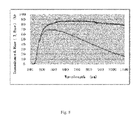
- FIG. 8 is a curve diagram of optical properties of a LPCVD BZO
- FIG. 9( a ) is a photo of a surface of a silicon wafer where a BZO thin film is deposited.
- FIG. 9( b ) is a photo of a surface of a silicon wafer that has been cleaned but not texturized yet.
- FIGS. 3 and 4 are respectively a schematic flowchart of a method of fabricating a heterojunction battery in the present invention and the schematic structural diagram of the same.
- a first amorphous silicon intrinsic layer 200 is deposited on the front of an n-type silicon wafer 100 , which n-type silicon wafer 100 here may be a monocrystal or polycrystal silicon wafer.
- n-type silicon wafer 100 Before depositing amorphous silicon intrinsic layer 200 , a surface of n-type silicon wafer 100 needs to be cleaned and cut-damaged, so as to fabricate a high-efficiency heterojunction battery on the smooth silicon wafer (damage removed).
- PECVD Plasma Enhanced Chemical Vapor Deposition
- the range of the thickness of first amorphous silicon intrinsic layer 200 is between 5 nm and 30 nm, e.g. 5 nm, 18 nm or 30 nm.
- an amorphous silicon p layer 300 is deposited on first amorphous silicon intrinsic layer 200 .
- PECVD method is used to deposit the amorphous silicon material to form amorphous silicon p layer 300 .
- the range of the thickness of amorphous silicon p layer 300 is between 5 nm and 30 nm, e.g. 5 nm, 18 nm or 30 nm.
- a first boron doped zinc oxide thin film (BZO) 400 is deposited on amorphous silicon p layer 300 .
- LPCVD Low Pressure Chemical Vapor Deposition
- the range of the thickness of first boron doped zinc oxide thin film (BZO) 400 is between 500 nm and 1000 nm, e.g. 500 nm, 750 nm or 1000 nm.
- first boron doped zinc oxide thin film 400 presents a pyramid structure; this structure has good light trapping effect and thus can completely replace texturization and relevant cleaning process in the traditional process.
- forming an anti-reflection film by depositing first boron doped zinc oxide thin film 400 in place of sputtering ITO (Indium Tin Oxide) can greatly reduce the usage amount of expensive ITO and further save the production cost.
- ITO Indium Tin Oxide
- a back electrode 620 and an Al-back surface field 500 are formed on the back of n-type silicon wafer 100 .
- Al-back surface field 500 may be formed by printing an aluminum paste on the back of n-type silicon wafer 100 by silk-screen printing method and then sintering it.
- a positive electrode 610 is formed on the front of n-type silicon wafer 100 .
- back electrode 620 and/or positive electrode 610 may be fabricated by printing silver paste or electrocoppering.
- back electrode 620 and/or positive electrode 610 may be formed using electroplating or silk-screen printing, etc.
- FIGS. 5 and 6 are respectively a schematic flowchart of the method of fabricating a double-sided heterojunction battery in the present invention and the schematic structural diagram of the same.
- a first amorphous silicon intrinsic layer 200 is deposited on the front of an n-type silicon wafer 100 .
- a surface of n-type silicon wafer 100 needs to be cleaned and cut-damaged, so as to fabricate a high-efficiency heterojunction battery on the smooth silicon wafer (damage removed).
- PECVD Plasma Enhanced Chemical Vapor Deposition
- the range of the thickness of first amorphous silicon intrinsic layer 200 is between 5 nm and 30 nm, e.g. 5 nm, 18 nm or 30 nm.
- an amorphous silicon p layer 300 is deposited on first amorphous silicon intrinsic layer 200 .
- PECVD method is adopted to deposit the amorphous silicon material to form amorphous silicon p layer 300 .
- the range of the thickness of amorphous silicon p layer 300 is between 5 nm and 30 nm, e.g. 5 nm, 18 nm or 30 nm.
- a second amorphous silicon intrinsic layer 210 is deposited on the back of n-type silicon wafer 100 .
- PECVD Pulsma Enhanced Chemical Vapor Deposition
- the range of the thickness of the second amorphous silicon intrinsic layer 210 is between 5 nm and 30 nm, e.g. 5 nm, 18 nm or 30 nm.
- an amorphous silicon n layer 700 is deposited on the back of second amorphous silicon intrinsic layer 210 .
- PECVD Pulsma Enhanced Chemical Vapor Deposition
- the range of the thickness of amorphous silicon n layer 700 is between 5 nm and 30 nm, e.g. 5 nm, 18 nm or 30 nm.
- a first boron doped zinc oxide thin film 400 is deposited on amorphous silicon p layer 300
- a second boron doped zinc oxide thin film 410 is deposited on amorphous silicon n layer 700 .
- LPCVD Low Pressure Chemical Vapor Deposition
- the range of the thickness of first boron doped zinc oxide thin film 400 is between 500 nm and 1000 nm. e.g. 500 nm, 750 nm or 1000 nm.
- a thickness range of second boron doped zinc oxide thin film 410 is between 500 nm and 1000 nm, e.g. 500 nm, 750 nm or 1000 nm.
- a surface of the boron doped zinc oxide thin film presents a pyramid structure; this structure has good light trapping effect and thus can completely replace texturization and relevant cleaning process in the traditional process.
- forming an antireflection film by depositing the boron doped zinc oxide thin films in place of sputtering ITO (Indium Tin Oxide) can greatly reduce the usage amount of expensive ITO and further save the production cost.
- ITO Indium Tin Oxide
- second boron doped Zinc oxide thin film 410 on amorphous silicon n layer 400 , good electric conduction effect can be produced on the back of the silicon wafer, which can replace an Al-back surface field.
- step S 206 a back electrode 620 is formed on the back of the n-type silicon wafer.
- a positive electrode 610 is formed on the front of the n-type silicon wafer.
- back electrode 620 and/or positive electrode 610 may be fabricated by printing silver paste or electrocoppering.
- back electrode 620 and/or positive electrode 610 may be formed using electroplating or silk-screen printing, etc.
- LPCVD-BZO boron doped zinc oxide
- TCO boron doped zinc oxide
- BZO is a transparent conductive material with a textured structure and has excellent light-trapping effect, and thus can replace the step of texturization; moreover, compared with common ITO, BZO is characterized by being low-cost, easy to fabricate and suitable for large scale production. Therefore, heterojunction batteries fabricated using the method of the present invention have a simple, reliable and low-cost process and a high photoelectric conversion efficiency, and moreover, are suitable for mass production.
Abstract
Description
Claims (13)
Applications Claiming Priority (3)
| Application Number | Priority Date | Filing Date | Title |
|---|---|---|---|
| CN2013101259023A CN103227246A (en) | 2013-04-11 | 2013-04-11 | Preparation method of heterojunction cell |
| CN201310125902 | 2013-04-11 | ||
| CN201310125902.3 | 2013-04-11 |
Publications (2)
| Publication Number | Publication Date |
|---|---|
| US20140308773A1 US20140308773A1 (en) | 2014-10-16 |
| US9023681B2 true US9023681B2 (en) | 2015-05-05 |
Family
ID=48837616
Family Applications (1)
| Application Number | Title | Priority Date | Filing Date |
|---|---|---|---|
| US14/036,542 Active US9023681B2 (en) | 2013-04-11 | 2013-09-25 | Method of fabricating heterojunction battery |
Country Status (2)
| Country | Link |
|---|---|
| US (1) | US9023681B2 (en) |
| CN (1) | CN103227246A (en) |
Families Citing this family (23)
| Publication number | Priority date | Publication date | Assignee | Title |
|---|---|---|---|---|
| CN104600130A (en) * | 2015-01-13 | 2015-05-06 | 福建铂阳精工设备有限公司 | Silicon-based thin-film solar cell and preparation method thereof |
| CN104600136A (en) * | 2015-01-13 | 2015-05-06 | 福建铂阳精工设备有限公司 | Manufacturing method of hetero-junction solar cell and hetero-junction solar cell |
| CN106328757A (en) * | 2015-07-06 | 2017-01-11 | 中海阳能源集团股份有限公司 | Method for processing heterojunction solar cell |
| CN105304765B (en) * | 2015-11-13 | 2017-08-29 | 新奥光伏能源有限公司 | A kind of silicon heterogenous solar cell and preparation method thereof |
| KR101821394B1 (en) * | 2016-01-14 | 2018-01-23 | 엘지전자 주식회사 | Solar cell |
| CN105957905A (en) * | 2016-06-21 | 2016-09-21 | 常州天合光能有限公司 | Crystalline silicon solar cell free of fine grid line and preparation method of crystalline silicon solar cell |
| CN109690791B (en) * | 2016-06-30 | 2022-09-16 | 株式会社钟化 | Crystalline silicon solar cell and method for manufacturing same |
| KR20180007585A (en) * | 2016-07-13 | 2018-01-23 | 엘지전자 주식회사 | Tandem solar cell, tanden solar cell module comprising the same and method for manufacturing thereof |
| CN106098835A (en) * | 2016-08-19 | 2016-11-09 | 山东新华联新能源科技有限公司 | Heterojunction solar battery and preparation method thereof |
| EP3503208A1 (en) * | 2017-12-21 | 2019-06-26 | Beijing Juntai Innovation Technology Co., Ltd | Thin film assembly and method of preparing the same, and hetero-junction solar cell including thin film assembly |
| CN109326673A (en) * | 2018-08-10 | 2019-02-12 | 浙江正泰太阳能科技有限公司 | P-type crystal silicon PERC battery and preparation method thereof |
| CN109378347A (en) * | 2018-09-19 | 2019-02-22 | 黄剑鸣 | A kind of heterojunction solar battery and preparation method thereof based on n-type silicon chip |
| CN109192865B (en) * | 2018-09-28 | 2022-04-15 | 苏州钱正科技咨询有限公司 | Silicon-based heterojunction solar cell with high contact area and preparation method thereof |
| CN110620163A (en) * | 2019-10-28 | 2019-12-27 | 成都晔凡科技有限公司 | Heterojunction solar cell, laminated tile assembly and manufacturing method thereof |
| CN110854219A (en) * | 2019-12-24 | 2020-02-28 | 浙江中晶新能源股份有限公司 | Efficient N-type battery piece and preparation method thereof |
| CN114203839A (en) * | 2020-11-11 | 2022-03-18 | 福建金石能源有限公司 | Manufacturing method of heterojunction solar single-sided battery |
| CN112614902A (en) * | 2020-11-27 | 2021-04-06 | 北京绿兴能源科技有限公司 | Composite structure transparent conductive film for heterojunction solar cell and preparation method thereof |
| CN114649422A (en) * | 2020-12-17 | 2022-06-21 | 浙江爱旭太阳能科技有限公司 | Silicon-based heterojunction solar cell structure and preparation method |
| CN114824263B (en) * | 2021-01-29 | 2024-03-19 | 中南大学 | Zn@Zn-E composite negative electrode, preparation method thereof and application thereof in water-based zinc ion battery |
| CN113471306A (en) * | 2021-06-01 | 2021-10-01 | 安徽华晟新能源科技有限公司 | Heterojunction battery and preparation method thereof |
| CN113990972B (en) * | 2021-12-28 | 2022-06-21 | 浙江爱旭太阳能科技有限公司 | Heterojunction battery for improving photoelectric conversion efficiency |
| CN114725246A (en) * | 2022-04-12 | 2022-07-08 | 安徽华晟新能源科技有限公司 | Preparation method of heterojunction battery and heterojunction battery |
| CN115394881A (en) * | 2022-09-30 | 2022-11-25 | 滁州捷泰新能源科技有限公司 | TOPCON battery with gradient distribution of phosphorus concentration and manufacturing method thereof |
Citations (1)
| Publication number | Priority date | Publication date | Assignee | Title |
|---|---|---|---|---|
| US20130210185A1 (en) * | 2010-10-01 | 2013-08-15 | Kaneka Corporation | Method for manufacturing photoelectric conversion device |
Family Cites Families (5)
| Publication number | Priority date | Publication date | Assignee | Title |
|---|---|---|---|---|
| US7119271B2 (en) * | 2001-10-12 | 2006-10-10 | The Boeing Company | Wide-bandgap, lattice-mismatched window layer for a solar conversion device |
| EP1643564B1 (en) * | 2004-09-29 | 2019-01-16 | Panasonic Intellectual Property Management Co., Ltd. | Photovoltaic device |
| CN104952943B (en) * | 2009-04-21 | 2017-07-18 | 泰特拉桑有限公司 | High efficiency solar cell structure and manufacture method |
| TW201218397A (en) * | 2010-07-09 | 2012-05-01 | Applied Materials Inc | High performance multi-layer back contact stack for silicon solar cells |
| CN103000741A (en) * | 2012-11-21 | 2013-03-27 | 国电光伏(江苏)有限公司 | Black heterogeneous crystalline cell and manufacture method thereof |
-
2013
- 2013-04-11 CN CN2013101259023A patent/CN103227246A/en active Pending
- 2013-09-25 US US14/036,542 patent/US9023681B2/en active Active
Patent Citations (1)
| Publication number | Priority date | Publication date | Assignee | Title |
|---|---|---|---|---|
| US20130210185A1 (en) * | 2010-10-01 | 2013-08-15 | Kaneka Corporation | Method for manufacturing photoelectric conversion device |
Also Published As
| Publication number | Publication date |
|---|---|
| US20140308773A1 (en) | 2014-10-16 |
| CN103227246A (en) | 2013-07-31 |
Similar Documents
| Publication | Publication Date | Title |
|---|---|---|
| US9023681B2 (en) | Method of fabricating heterojunction battery | |
| CN109004053B (en) | Crystalline silicon/thin film silicon heterojunction solar cell with double-sided light receiving function and manufacturing method thereof | |
| CN110993700A (en) | Heterojunction solar cell and preparation process thereof | |
| US10084107B2 (en) | Transparent conducting oxide for photovoltaic devices | |
| CN205863192U (en) | A kind of silicon based hetero-junction solaode using double TCO film layer | |
| TWI463682B (en) | Heterojunction solar cell having intrinsic amorphous silicon film | |
| CN102270705B (en) | Method for preparing transparent conductive electrode with dual-structure texture surface | |
| CN101976710A (en) | Method for preparing crystalline silicon hetero-junction solar cell based on hydrogenated microcrystalline silicon film | |
| CN103000741A (en) | Black heterogeneous crystalline cell and manufacture method thereof | |
| CN110416328A (en) | A kind of HJT battery and preparation method thereof | |
| CN203503678U (en) | HIT solar cell | |
| CN102364692A (en) | Double side light receiving crystalline silicon solar cell with fully-passivated structure and manufacturing method thereof | |
| WO2022247570A1 (en) | Heterojunction solar cell and preparation method therefor | |
| CN1949545A (en) | New structure crystal silicon solar energy battery | |
| CN102270668B (en) | Heterojunction solar cell and preparation method thereof | |
| CN108735828A (en) | A kind of hetero-junctions back contact solar cell and preparation method thereof | |
| CN205960004U (en) | High -efficient heterojunction solar cell | |
| TW201010115A (en) | Method for depositing an amorphous silicon film for photovoltaic devices with reduced light-induced degradation for improved stabilized performance | |
| CN111435693A (en) | Amorphous silicon/crystalline silicon heterojunction solar cell and preparation method thereof | |
| CN210156405U (en) | Heterojunction cell structure with hydrogen annealed TCO conductive film | |
| CN108538937B (en) | Solar cell and preparation method thereof | |
| CN208521944U (en) | A kind of hetero-junctions back contact solar cell | |
| CN103165695B (en) | A kind of CdTe thin film solar cell | |
| CN112701194A (en) | Preparation method of heterojunction solar cell | |
| CN112366232B (en) | Heterojunction solar cell and preparation method and application thereof |
Legal Events
| Date | Code | Title | Description |
|---|---|---|---|
| AS | Assignment |
Owner name: CHINT SOLAR (ZHEJIANG)CO.,LTD., CHINA Free format text: ASSIGNMENT OF ASSIGNORS INTEREST;ASSIGNORS:NIU, XINWEI;YU, CAO;DING, LAN;AND OTHERS;REEL/FRAME:031278/0212 Effective date: 20130925 |
|
| STCF | Information on status: patent grant |
Free format text: PATENTED CASE |
|
| FEPP | Fee payment procedure |
Free format text: SURCHARGE FOR LATE PAYMENT, SMALL ENTITY (ORIGINAL EVENT CODE: M2554); ENTITY STATUS OF PATENT OWNER: SMALL ENTITY |
|
| MAFP | Maintenance fee payment |
Free format text: PAYMENT OF MAINTENANCE FEE, 4TH YR, SMALL ENTITY (ORIGINAL EVENT CODE: M2551); ENTITY STATUS OF PATENT OWNER: SMALL ENTITY Year of fee payment: 4 |
|
| AS | Assignment |
Owner name: CHINT NEW ENERGY TECHNOLOGY CO., LTD., CHINA Free format text: CHANGE OF NAME;ASSIGNOR:CHINT SOLAR (ZHEJIANG) CO., LTD.;REEL/FRAME:059878/0848 Effective date: 20130925 |
|
| FEPP | Fee payment procedure |
Free format text: ENTITY STATUS SET TO UNDISCOUNTED (ORIGINAL EVENT CODE: BIG.); ENTITY STATUS OF PATENT OWNER: LARGE ENTITY |
|
| MAFP | Maintenance fee payment |
Free format text: PAYMENT OF MAINTENANCE FEE, 8TH YEAR, LARGE ENTITY (ORIGINAL EVENT CODE: M1552); ENTITY STATUS OF PATENT OWNER: LARGE ENTITY Year of fee payment: 8 |