US9001054B2 - Image display device - Google Patents
Image display device Download PDFInfo
- Publication number
- US9001054B2 US9001054B2 US13/280,420 US201113280420A US9001054B2 US 9001054 B2 US9001054 B2 US 9001054B2 US 201113280420 A US201113280420 A US 201113280420A US 9001054 B2 US9001054 B2 US 9001054B2
- Authority
- US
- United States
- Prior art keywords
- touch panel
- image display
- terminal electrodes
- printed circuit
- flexible printed
- Prior art date
- Legal status (The legal status is an assumption and is not a legal conclusion. Google has not performed a legal analysis and makes no representation as to the accuracy of the status listed.)
- Active, expires
Links
- 239000000758 substrate Substances 0.000 claims abstract description 33
- 229920005989 resin Polymers 0.000 claims description 31
- 239000011347 resin Substances 0.000 claims description 31
- 230000009477 glass transition Effects 0.000 claims description 19
- 230000002950 deficient Effects 0.000 claims description 4
- 239000004973 liquid crystal related substance Substances 0.000 abstract description 85
- 101000931374 Homo sapiens Zinc finger protein ZFPM1 Proteins 0.000 abstract description 10
- 102100020993 Zinc finger protein ZFPM1 Human genes 0.000 abstract description 10
- 101000931371 Homo sapiens Zinc finger protein ZFPM2 Proteins 0.000 abstract 1
- 102100020996 Zinc finger protein ZFPM2 Human genes 0.000 abstract 1
- 239000010408 film Substances 0.000 description 54
- 238000010586 diagram Methods 0.000 description 29
- 101000763003 Homo sapiens Two pore channel protein 1 Proteins 0.000 description 13
- 101000679525 Homo sapiens Two pore channel protein 2 Proteins 0.000 description 13
- 102100026736 Two pore channel protein 1 Human genes 0.000 description 13
- 102100022609 Two pore channel protein 2 Human genes 0.000 description 13
- 101000653679 Homo sapiens Translationally-controlled tumor protein Proteins 0.000 description 11
- ZBZXYUYUUDZCNB-UHFFFAOYSA-N N-cyclohexa-1,3-dien-1-yl-N-phenyl-4-[4-(N-[4-[4-(N-[4-[4-(N-phenylanilino)phenyl]phenyl]anilino)phenyl]phenyl]anilino)phenyl]aniline Chemical compound C1=CCCC(N(C=2C=CC=CC=2)C=2C=CC(=CC=2)C=2C=CC(=CC=2)N(C=2C=CC=CC=2)C=2C=CC(=CC=2)C=2C=CC(=CC=2)N(C=2C=CC=CC=2)C=2C=CC(=CC=2)C=2C=CC(=CC=2)N(C=2C=CC=CC=2)C=2C=CC=CC=2)=C1 ZBZXYUYUUDZCNB-UHFFFAOYSA-N 0.000 description 11
- 102100029887 Translationally-controlled tumor protein Human genes 0.000 description 11
- JXSJBGJIGXNWCI-UHFFFAOYSA-N diethyl 2-[(dimethoxyphosphorothioyl)thio]succinate Chemical compound CCOC(=O)CC(SP(=S)(OC)OC)C(=O)OCC JXSJBGJIGXNWCI-UHFFFAOYSA-N 0.000 description 7
- OFHWSHGIZXHMJP-UHFFFAOYSA-N 1,3,5-tripropyl-1,3,5-triazinane-2,4,6-trione Chemical compound CCCN1C(=O)N(CCC)C(=O)N(CCC)C1=O OFHWSHGIZXHMJP-UHFFFAOYSA-N 0.000 description 4
- 238000000034 method Methods 0.000 description 2
- 239000004840 adhesive resin Substances 0.000 description 1
- 229920006223 adhesive resin Polymers 0.000 description 1
- 230000001413 cellular effect Effects 0.000 description 1
- 230000010354 integration Effects 0.000 description 1
- 230000002452 interceptive effect Effects 0.000 description 1
- 238000004519 manufacturing process Methods 0.000 description 1
- 239000002245 particle Substances 0.000 description 1
- 239000010409 thin film Substances 0.000 description 1
- 230000003245 working effect Effects 0.000 description 1
Images


Classifications
-
- H—ELECTRICITY
- H05—ELECTRIC TECHNIQUES NOT OTHERWISE PROVIDED FOR
- H05K—PRINTED CIRCUITS; CASINGS OR CONSTRUCTIONAL DETAILS OF ELECTRIC APPARATUS; MANUFACTURE OF ASSEMBLAGES OF ELECTRICAL COMPONENTS
- H05K1/00—Printed circuits
- H05K1/02—Details
- H05K1/0277—Bendability or stretchability details
- H05K1/028—Bending or folding regions of flexible printed circuits
-
- G—PHYSICS
- G02—OPTICS
- G02F—OPTICAL DEVICES OR ARRANGEMENTS FOR THE CONTROL OF LIGHT BY MODIFICATION OF THE OPTICAL PROPERTIES OF THE MEDIA OF THE ELEMENTS INVOLVED THEREIN; NON-LINEAR OPTICS; FREQUENCY-CHANGING OF LIGHT; OPTICAL LOGIC ELEMENTS; OPTICAL ANALOGUE/DIGITAL CONVERTERS
- G02F1/00—Devices or arrangements for the control of the intensity, colour, phase, polarisation or direction of light arriving from an independent light source, e.g. switching, gating or modulating; Non-linear optics
- G02F1/01—Devices or arrangements for the control of the intensity, colour, phase, polarisation or direction of light arriving from an independent light source, e.g. switching, gating or modulating; Non-linear optics for the control of the intensity, phase, polarisation or colour
- G02F1/13—Devices or arrangements for the control of the intensity, colour, phase, polarisation or direction of light arriving from an independent light source, e.g. switching, gating or modulating; Non-linear optics for the control of the intensity, phase, polarisation or colour based on liquid crystals, e.g. single liquid crystal display cells
- G02F1/133—Constructional arrangements; Operation of liquid crystal cells; Circuit arrangements
- G02F1/1333—Constructional arrangements; Manufacturing methods
- G02F1/133308—Support structures for LCD panels, e.g. frames or bezels
-
- G—PHYSICS
- G02—OPTICS
- G02F—OPTICAL DEVICES OR ARRANGEMENTS FOR THE CONTROL OF LIGHT BY MODIFICATION OF THE OPTICAL PROPERTIES OF THE MEDIA OF THE ELEMENTS INVOLVED THEREIN; NON-LINEAR OPTICS; FREQUENCY-CHANGING OF LIGHT; OPTICAL LOGIC ELEMENTS; OPTICAL ANALOGUE/DIGITAL CONVERTERS
- G02F1/00—Devices or arrangements for the control of the intensity, colour, phase, polarisation or direction of light arriving from an independent light source, e.g. switching, gating or modulating; Non-linear optics
- G02F1/01—Devices or arrangements for the control of the intensity, colour, phase, polarisation or direction of light arriving from an independent light source, e.g. switching, gating or modulating; Non-linear optics for the control of the intensity, phase, polarisation or colour
- G02F1/13—Devices or arrangements for the control of the intensity, colour, phase, polarisation or direction of light arriving from an independent light source, e.g. switching, gating or modulating; Non-linear optics for the control of the intensity, phase, polarisation or colour based on liquid crystals, e.g. single liquid crystal display cells
- G02F1/133—Constructional arrangements; Operation of liquid crystal cells; Circuit arrangements
- G02F1/1333—Constructional arrangements; Manufacturing methods
- G02F1/13338—Input devices, e.g. touch panels
-
- H—ELECTRICITY
- H05—ELECTRIC TECHNIQUES NOT OTHERWISE PROVIDED FOR
- H05K—PRINTED CIRCUITS; CASINGS OR CONSTRUCTIONAL DETAILS OF ELECTRIC APPARATUS; MANUFACTURE OF ASSEMBLAGES OF ELECTRICAL COMPONENTS
- H05K1/00—Printed circuits
- H05K1/02—Details
- H05K1/14—Structural association of two or more printed circuits
- H05K1/147—Structural association of two or more printed circuits at least one of the printed circuits being bent or folded, e.g. by using a flexible printed circuit
-
- G—PHYSICS
- G02—OPTICS
- G02F—OPTICAL DEVICES OR ARRANGEMENTS FOR THE CONTROL OF LIGHT BY MODIFICATION OF THE OPTICAL PROPERTIES OF THE MEDIA OF THE ELEMENTS INVOLVED THEREIN; NON-LINEAR OPTICS; FREQUENCY-CHANGING OF LIGHT; OPTICAL LOGIC ELEMENTS; OPTICAL ANALOGUE/DIGITAL CONVERTERS
- G02F1/00—Devices or arrangements for the control of the intensity, colour, phase, polarisation or direction of light arriving from an independent light source, e.g. switching, gating or modulating; Non-linear optics
- G02F1/01—Devices or arrangements for the control of the intensity, colour, phase, polarisation or direction of light arriving from an independent light source, e.g. switching, gating or modulating; Non-linear optics for the control of the intensity, phase, polarisation or colour
- G02F1/13—Devices or arrangements for the control of the intensity, colour, phase, polarisation or direction of light arriving from an independent light source, e.g. switching, gating or modulating; Non-linear optics for the control of the intensity, phase, polarisation or colour based on liquid crystals, e.g. single liquid crystal display cells
- G02F1/133—Constructional arrangements; Operation of liquid crystal cells; Circuit arrangements
- G02F1/1333—Constructional arrangements; Manufacturing methods
- G02F1/1345—Conductors connecting electrodes to cell terminals
- G02F1/13452—Conductors connecting driver circuitry and terminals of panels
-
- H—ELECTRICITY
- H05—ELECTRIC TECHNIQUES NOT OTHERWISE PROVIDED FOR
- H05K—PRINTED CIRCUITS; CASINGS OR CONSTRUCTIONAL DETAILS OF ELECTRIC APPARATUS; MANUFACTURE OF ASSEMBLAGES OF ELECTRICAL COMPONENTS
- H05K2201/00—Indexing scheme relating to printed circuits covered by H05K1/00
- H05K2201/05—Flexible printed circuits [FPCs]
- H05K2201/053—Tails
-
- H—ELECTRICITY
- H05—ELECTRIC TECHNIQUES NOT OTHERWISE PROVIDED FOR
- H05K—PRINTED CIRCUITS; CASINGS OR CONSTRUCTIONAL DETAILS OF ELECTRIC APPARATUS; MANUFACTURE OF ASSEMBLAGES OF ELECTRICAL COMPONENTS
- H05K3/00—Apparatus or processes for manufacturing printed circuits
- H05K3/36—Assembling printed circuits with other printed circuits
- H05K3/361—Assembling flexible printed circuits with other printed circuits
Definitions
- the present invention relates to an image display device, and in particular to an image display device having an image display panel, such as a liquid crystal panel or an organic electroluminescent panel, and a touch panel.
- an image display panel such as a liquid crystal panel or an organic electroluminescent panel, and a touch panel.
- Thin image display devices such as liquid crystal modules (liquid crystal display devices) and organic electroluminescent modules (organic EL display devices), are used for the display devices of many portable information apparatuses, such as cellular phones, personal data assistants (PDAs), digital cameras and multimedia players.
- portable information apparatuses such as cellular phones, personal data assistants (PDAs), digital cameras and multimedia players.
- PDAs personal data assistants
- FIG. 1 is a perspective diagram showing an example of a liquid crystal display device that is formed of a liquid crystal panel and a backlight unit BLU for illuminating the liquid crystal panel.
- DA represents the display region of the liquid crystal panel.
- the liquid crystal panel has a TFT substrate (TFTS) on which switching elements made of thin film transistors and electrodes are provided and a color filter substrate (facing substrate, CFS) on which color filters are formed, and liquid crystal is sealed in between the TFT substrate and the color filter substrate.
- a driver chip (DRC) for driving the liquid crystal panel is mounted on part of the TFT substrate.
- the liquid crystal panel has an upper polarizing plate (UPP) provided on the upper side of the color filter substrate and a lower polarizing plate (not shown) provided on the lower side of the TFT substrate.
- the wires connected to the liquid crystal panel are included in a flexible printed circuit (FPC) as shown in FIG. 1 .
- the organic EL display device also uses a TFT substrate where the wires are connected in an FPC.
- FIG. 2 is a perspective diagram showing a touch panel where touch panel electrodes (TPE) are formed on one side of a touch panel substrate (transparent substrate, TPS).
- TPE touch panel electrodes
- TPS transparent substrate
- the wires connected to the touch panel are included in a flexible printed circuit (FPC) on which a driving IC for driving the touch panel is mounted.
- IFT represents the interface of the flexible printed circuit.
- FIG. 3 shows an example of a liquid crystal display device having a touch panel.
- a front panel (FW) for protecting a liquid crystal panel LCP and a touch panel TP are provided, and the touch panel TP and the liquid crystal panel LCP are provided in this order on the rear surface.
- the touch panel and the liquid crystal panel are provided in proximity, and therefore there are many wires in a small space which makes it difficult to make the liquid crystal display device thinner.
- organic EL display devices arises in organic EL display devices.
- JP 2003-280541A discloses a number of liquid crystal panels that are implemented by using one flexible printed circuit in order to provide display devices on the two sides, front and rear.
- the present inventor examined the method for implementing a touch panel and a liquid crystal panel connected through one flexible printed circuit and found that there is no space for the backlight between the touch panel and the liquid crystal panel as in JP 2003-280541A. Therefore, the distance between the terminals for the liquid crystal panel on the flexible printed circuit and the terminals for the touch panel is short, which makes it difficult to connect the flexible printed circuit to the liquid crystal panel and the touch panel with high precision.
- connection between the flexible printed circuit and the liquid crystal panel is made by an FOG contact bond where the two are connected through the application of pressure and heat with an anisotropic conductive film in between. Therefore, the flexible printed circuit is connected to one panel, and after that the flexible printed circuit is connected to the other panel when it is found that the previous connection might slide or disengage due to the heat applied for the FOG contact bond, which leads to a problem.
- JP 2005-38231A discloses a touch panel attached to one branch of an FPC and a liquid crystal display device attached to the other branch in order to reduce the number of connection cables so that the cost for parts and cost for assembly can be reduced. Furthermore, JP 2005-38231A discloses a touch panel and a liquid crystal display device that are integrated.
- An object of the present invention is to solve the above-described problems and provide an image display device where an image display panel and a touch panel are connected through wires in one flexible printed circuit in such a manner that the image display panel and the touch panel are connected through wires with high precision, and no problems arise, such as the portion that has once been connected disengaging.
- the invention makes the following means available.
- An image display device having an image display panel and a touch panel provided on the front surface of the image display panel, characterized in that wires connected to the image display panel and wires connected to the touch panel are provided in one flexible printed circuit, and the flexible printed circuit is first connected to terminals in the image display panel and then connected to terminals in the touch panel.
- the flexible printed circuit is connected to the image display panel and the touch panel using anisotropic conductive films, and the glass transition temperature of the resin that forms the anisotropic conductive film used for the connection between the image display panel and the flexible printed circuit is higher than that of the anisotropic conductive film used for the connection between the touch panel and the flexible printed circuit.
- the image display device according to the above (1) or (2), characterized in that the touch panel has terminal electrodes provided on the two sides, front and rear, of the touch panel substrate, and wires connected to the terminal electrodes on each side of the touch panel are provided in the flexible printed circuit.
- An image display device having an image display panel and a touch panel provided on the front surface of the image display panel, characterized in that the touch panel has front terminal electrodes provided on the front surface of the touch panel substrate and rear terminal electrodes provided on the rear surface of the touch panel substrate, the touch panel comprises wires connected to the front terminal electrodes and the rear terminal electrodes in one flexible printed circuit, and the front terminal electrodes and the rear terminal electrodes on the touch panel are respectively connected to the flexible printed circuit using anisotropic conductive films in such a manner that the glass transition temperature of the resin that forms the anisotropic conductive film is different between the anisotropic conductive film used for the front terminal electrodes and the anisotropic conductive film used for the rear terminal electrodes.
- the image display device characterized in that the image display panel and the touch panel are made to make close contact with each other with a transparent resin layer in between.
- the image display device further comprises a front panel, which is made to make close contact with the touch panel with a transparent resin layer in between.
- the front terminal electrodes and the rear terminal electrodes are provided along the same side when the touch panel is viewed from the top.
- the image display device characterized in that the image display panel and the touch panel are connected through one flexible printed circuit, the image display panel and the flexible printed circuit are connected through a first anisotropic conductive film, front terminal electrodes of the touch panel and the flexible printed circuit are connected through a second anisotropic conductive film, rear terminal electrodes of the touch panel and the flexible printed circuit are connected through a third anisotropic conductive film, the glass transition temperature of the resin that forms the anisotropic conductive film is different between the second anisotropic conductive film and the third anisotropic conductive film, and the front terminal electrodes and the rear terminal electrodes are located in different places, and the second anisotropic film and the third anisotropic conductive film are located in different places when the touch panel is viewed from the top.
- the image display device characterized in that the front terminal electrodes and the rear terminal electrodes are respectively formed of a number of terminals in such a manner that the intervals at which the terminals are located are smaller for the front terminal electrodes than for the rear terminal electrodes, and the glass transition temperature of the resin that forms the second anisotropic conductive film is higher than the glass transition temperature of the resin that forms the third anisotropic conductive film.
- one flexible printed circuit has wires connected to an image display panel and wires connected to a touch panel in such a manner that the flexible printed circuit is first connected to the image display panel and then connected to the touch panel.
- the flexible printed circuit is connected with high precision to the image display panel where the intervals between the wires is smaller, and then the flexible printed circuit is connected to the touch panel where the intervals between the wires is greater than in the image display panel, and thus the connections to the flexible printed circuit can be prevented from being defective.
- the flexible printed circuit is connected to the image display panel and the touch panel using anisotropic conductive films where the glass transition temperature of the resin that forms the anisotropic conductive film is higher for the anisotropic conductive film used for the connection to the image display panel than for the anisotropic conductive film used for the connection to the touch panel, and therefore it is possible to prevent such a problem as the previous connection to the liquid crystal panel disengaging from occurring when the touch panel and the flexible printed circuit are connected to each other.
- FIG. 1 is a perspective diagram showing a conventional liquid crystal display device
- FIG. 2 is a perspective diagram showing a touch panel
- FIG. 3 is a cross-sectional diagram showing a conventional liquid crystal display device having a liquid crystal panel and a touch panel;
- FIG. 4 is a cross-sectional diagram showing the image display device according to the present invention having a liquid crystal panel, which is an image display panel, and a touch panel;
- FIG. 5 is a plan diagram showing a flexible printed circuit used in the image display device according to the present invention (in the case where terminals for the image display panel LCPT and terminals for the touch panel TPT are located along the facing sides);
- FIG. 6 is a plan diagram showing a flexible printed circuit used in the image display device according to the present invention (in the case where terminals for the image display panel LCPT and terminals for the touch panel TPT are located along sides on the same side);
- FIG. 7 is a perspective diagram showing a touch panel having electrodes for the touch panel on the two sides;
- FIG. 8 is a cross-sectional diagram showing the touch panel in FIG. 7 ;
- FIG. 9 is a plan diagram showing a flexible printed circuit used for the touch panel shown in FIGS. 7 and 8 ;
- FIG. 10 is a cross-sectional diagram showing an image display device having the touch panel shown in FIG. 7 ;
- FIG. 11 is a plan diagram showing a flexible printed circuit used in the image display device shown in FIG. 10 (in the case where terminals for the image display panel LCPT and terminals for the touch panel TPT 1 are located along the facing sides);
- FIG. 12 is a plan diagram showing a flexible printed circuit used in the image display device shown in FIG. 10 (in the case where terminals for the image display panel LCPT and terminals for the touch panel TPT 1 are located along sides on the same side);
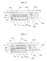
- FIG. 13 is a cross-sectional diagram showing an image display device where a liquid crystal panel, which is an image display panel, and a touch panel are made to make close contact with each other with a transparent resin layer in between;
- FIG. 14 is a cross-sectional diagram showing an image display device where the front panel and the touch panel are made to make close contact with the image display panel with a transparent resin layer in between;
- FIG. 15 is a cross-sectional diagram showing an image display device where a touch panel is incorporated into part of an image display panel
- FIG. 16 is a cross-sectional diagram showing the structure of the image display device shown in FIG. 15 with which a front panel is made to make contact with a transparent resin layer in between;
- FIG. 17 is a perspective diagram showing a touch panel used in the image display device according to the present invention.
- FIG. 18 is a plan diagram showing a flexible printed circuit used for the touch panel in FIG. 17 ;
- FIG. 19 is a perspective diagram showing a touch panel substrate used for the touch panel in FIG. 17 .
- the image display device is a liquid crystal display device having a liquid crystal panel LCP and a touch panel TP provided on the front surface of the liquid crystal panel is characterized in that wires connected to the liquid crystal panel and wires connected to the touch panel are included in one flexible printed circuit FPC, which is first connected (FOG 1 ) to the liquid crystal panel (specifically, a TFT substrate (TFTS)) and then connected (FOG 2 ) to the touch panel.
- FPC flexible printed circuit
- the image display device is described using a liquid crystal display device as an example.
- the image display device is not limited to a liquid crystal display device and may be other image display devices, such as an organic electroluminescent display device. Therefore, the liquid crystal panel in the following description may be other image display panels.
- the flexible printed circuit and the liquid crystal panel which is an image display panel
- the flexible printed circuit and the touch panel are connected to each other.
- the flexible printed circuit is connected to the touch panel of which the task is hindered by the liquid crystal panel connected to the flexible printed circuit.
- the intervals between the wires on the touch panel are greater that on the liquid crystal panel, and therefore no connections become defective even when the connections slide somewhat.
- the connections of the flexible printed circuit to the liquid crystal panel and the touch panel can be prevented from being defective.
- the liquid crystal panel LCP which is an image display panel, has image display panel terminal electrodes for the connection with the flexible printed circuit FPC, whereas the touch panel TP has touch panel terminal electrodes TPC (TPC 1 and TPC 2 , see FIG. 19 ) for the connection with the flexible printed circuit FPC.
- the flexible printed circuit FPC has terminals for the image display panel LCPT for the connection with the image display panel terminal electrodes and terminals for the touch panel TPT for the connection with the touch panel terminal electrodes TPC (see FIG. 5 ).
- the flexible printed circuit FPC is connected to the liquid crystal panel and the touch panel using anisotropic conductive films, where the glass transition temperature Tg of the resin that forms the anisotropic conductive film is higher for the first anisotropic conductive film (FOG 1 ) used for the connection between the liquid crystal panel and the flexible printed circuit than for the second anisotropic conductive film (FOG 2 ) used for the connection between the touch panel and the flexible printed circuit.
- Tg of the resin that forms the anisotropic conductive film is higher for the first anisotropic conductive film (FOG 1 ) used for the connection between the liquid crystal panel and the flexible printed circuit than for the second anisotropic conductive film (FOG 2 ) used for the connection between the touch panel and the flexible printed circuit.
- the anisotropic conductive films have such a structure that conductive particles are dispersed within an insulating and adhesive resin film. According to the method for adhesion using an anisotropic conductive film, an anisotropic conductive film is intervened between the liquid crystal panel, which is an image display panel, and the flexible printed circuit or between the touch panel and the flexible printed circuit, and a press head heated to approximately 180° C. is pressed against the connection portion so that the two are connected to each other.
- the glass transition temperature of the resin that forms the anisotropic conductive film is higher for the anisotropic conductive film used for the connection with the liquid crystal panel than for the anisotropic conductive film used for the connection with the touch panel, and therefore it is possible to prevent such a problem that the previous connection with the liquid crystal panel disengages or slides from occurring due to the heat for the connection between the touch panel and the flexible printed circuit after the connection with the liquid crystal panel.
- FIGS. 7 to 9 the embodiment shown in FIGS. 7 to 9 is described, where wires are connected to a touch panel through electrodes (TPE 1 , TPE 2 ) provided on the two sides of a touch panel substrate (TPS) in such a manner that the wires are included in one flexible printed circuit FPC.
- TPE 1 , TPE 2 touch panel substrate
- FIGS. 7 and 8 are a perspective diagram ( FIG. 7 ) and a cross-sectional diagram ( FIG. 8 ) showing a touch panel having electrodes for the touch panel (TPE 1 , TPE 2 ) on the two sides of a touch panel substrate (TPS) formed of an insulating substrate having high transparency for light.
- the plan diagram of FIG. 9 shows an example of a flexible printed circuit used for the touch panel in FIG. 7 .
- a driving IC (TPIC) for driving the touch panel is mounted on part of the flexible printed circuit.
- two portions of terminals TPT 1 and TPT 2 are provided on the flexible printed circuit as the terminals for the touch panel connected to the electrodes on the two sides, front and rear, of the touch panel.
- the connection between the touch panel and the flexible printed circuit is FOG contact bonds using anisotropic conductive films.
- FIGS. 17 to 19 show a touch panel having electrodes for the touch panel (TPE 1 ) on the two sides of the touch panel substrate TPS in the same manner as in FIG. 7 .
- the touch panel terminal electrodes TPC on the touch panel TP include front terminal electrodes TPC 1 provided on the front surface of the touch panel substrate and rear terminal electrodes TPC 2 provided on the rear surface of the touch panel.
- the front terminal electrodes TPC 1 on the touch panel are connected to the flexible printed circuit FPC through a second anisotropic conductive film FOG 2
- the rear terminal electrodes TPC 2 on the touch panel are connected to the flexible printed circuit FPC through a third anisotropic conductive film FOG 3 .
- the glass transition temperature of the resin that forms the anisotropic conductive film is different between the second anisotropic conductive film FOG 2 and the third anisotropic conductive film FOG 3 .
- FIG. 10 is a cross-sectional diagram showing the liquid crystal display device with a touch panel having electrodes for the touch panel on the two sides shown in FIG. 7 .
- Flexible printed circuits that can be used in the liquid crystal display device in FIG. 10 include those where terminals for the liquid crystal panel (LCPT) and terminals for the touch panel (TPT 1 ) are located along the facing sides as in FIG. 11 and those where terminals for the liquid crystal panel (LCPT) and terminals for the touch panel (TPT 1 ) are located along sides on the same side as in FIG. 12 .
- the intervals of the wires for the connection on the touch panel are smaller for those represented by TPT 1 than those represented by TPT 2 .
- the terminals to be connected to the wires with smaller intervals should be provided along the outer periphery of the flexible printed circuit as represented by TPT 1 in order to increase the efficiency for the connection task.
- the flexible printed circuit has connection terminals in three locations, LCPT, TPT 1 and TPT 2 . Therefore, the terminals for the liquid crystal panel (LCPT) are connected to the liquid crystal panel, and then the touch panel is connected.
- LCPT liquid crystal panel
- the glass transition temperature Tg of the resin that forms the anisotropic conductive film (FOG 1 to FOG 3 in FIG. 3 ) is always higher for the anisotropic conductive film used for the first connection than that of the anisotropic conductive film used for the following connection (FOG 1 >FOG 2 >FOG 3 for Tg).
- the liquid crystal panel (LCP) and the touch panel (TP) to be made to make close contact with a transparent resin layer (TR 1 ) in between, and in addition, as shown in FIG. 14 , it is possible for the front panel (FW) and the touch panel to be made to make close contact with a transparent resin layer (TR 2 ) in between.
- the thickness of the liquid crystal display device as a whole can be reduced, and in addition the mechanical strength of the display device as a whole can be increased.
- an advantage of the connection between the liquid crystal panel LCP and the touch panel TP using one flexible printed circuit FPC can be used in the integration of a circuit for driving the touch panel TP into the driver chip (DRC 1 ) mounted on the liquid crystal panel so that the driving IC for the touch panel can be omitted, which makes it possible to reduce the number of parts and the cost for manufacture.
- the driving IC (TPIC) for driving the touch panel is mounted on the part of the flexible printed circuit FPC that is the farthest from the front panel FW in the direction of the thickness of the liquid crystal display device (upward and downward direction in the figure).
- the driving IC (TPIC) can be prevented from interfering with the front panel (FW) due to its position, which contributes to the reduction in the thickness of the device as a whole.
- FIG. 15 is a cross-sectional diagram showing a liquid crystal display device where a touch panel is integrated into part of a liquid crystal panel LCP.
- electrodes for the touch panel TPE
- CFS color filter substrate
- terminal electrodes TPC are connected to the electrodes for the touch panel
- the terminal electrodes TPC and the flexible printed circuit FPC are connected through an FOG contact bond (FOG 2 ).
- a circuit for driving the touch panel TP is integrated in the driver chip (DRC 1 ) mounted on the liquid crystal panel in the same manner as in the embodiment in FIG. 13 .
- FIG. 16 shows the liquid crystal display device in FIG. 15 to which the structure for making the front panel (FW) make close contact with the liquid crystal panel with a transparent resin layer (TR 2 ) in between.
- the structure in FIG. 16 makes it possible to further increase the advantage of the liquid crystal display panel where the thickness is reduced by integrating the touch panel into the liquid crystal panel.
- the driving IC (TPIC) for driving the touch panel is mounted on the part of the flexible printed circuit FPC that is the farthest from the front panel (FW) in the direction of the thickness (upward and downward direction in the figure) of the liquid crystal display device in the same manner as in the embodiment in FIG. 14 .
- FIG. 17 is a perspective diagram showing a touch panel substrate TPS to which a flexible printed circuit FPC is connected. This is different from that in FIG. 7 in the location where the terminals for the touch panel TPT on the flexible printed circuit are connected to the touch panel terminal electrodes TPC on the touch panel TP. In FIG. 17 , the location along a side where the terminals for the touch panel TPT are connected to the touch panel terminal electrodes TPC is different between the upper side of the touch panel and the lower side of the touch panel when the touch panel having the flexible printed circuit is viewed from the top.
- FIG. 18 is a plan diagram showing the flexible printed circuit FPC in FIG. 17 where first terminals for the touch panel TPT 1 and second terminals for the touch panel TPT 2 are along the facing sides.
- the first terminals for the touch panel TPT 1 on the flexible printed circuit are first connected to the front terminal electrodes TPC 1 in FIG. 19 , and then the portion with the second terminals for the touch panel TPT 2 is folded back in order to be connected to the rear terminal electrodes TPC 2 .
- the touch panel terminal electrodes TPC on the touch panel TP include front terminal electrodes TPC 1 provided on the front surface of the touch panel substrate TPS and rear terminal electrodes TPC 2 provided on the rear surface of the touch panel substrate TPS in the same manner as in FIGS. 7 and 8 .
- the front surface is the side where the observer sees an image displayed on the image display device
- the rear surface is the image display panel side.
- the front terminal electrodes TPC 1 are connected to the flexible printed circuit through a second anisotropic conductive film FOG 2 while the rear terminal electrodes TPC 2 are connected to the flexible printed circuit through a third anisotropic conductive film FOG 3 in the same manner as in FIG. 10 .
- the front terminal electrodes TPC 1 and the rear terminal electrodes TPC 2 are located along the same side when viewed from the top. This structure makes the interface IFT of the flexible printed circuit FPC be concentrated in one portion, which makes the connection with an external apparatus easier.
- FIG. 19 is a perspective diagram showing the substrate TPS of the touch panel TP in FIG. 17 where the direction of the short sides of the rectangular touch panel is the direction X, the direction of the long sides is the direction Y and the direction of the thickness is the direction Z.
- the front terminal electrodes TPC 1 and the rear terminal electrodes TPC 2 on the touch panel are along a side in the direction X in different locations.
- the front terminal electrodes TPC 1 are connected to the front electrodes TPE 1 that form the touch panel, whereas the rear terminal electrodes TPC 2 are connected to the rear electrodes TPE 2 that form the touch panel.
- the front electrodes TPE 1 are touch panel electrodes made of electrodes running in the direction X and in the direction Y, for example.
- the rear electrodes TPE 2 are a transparent conductive film for shielding the noise emitted by the display panel, for example.
- the front terminal electrodes TPC 1 on the touch panel and the first terminals for the touch panel TPT 1 on the flexible printed circuit FPC are connected through the second anisotropic conductive film FOG 2
- the rear terminal electrodes TPC 2 on the touch panel and the second terminals for the touch panel TPT 2 on the flexible printed circuit FPC are connected through the third anisotropic conductive film FOG 3 .
- the front terminal electrodes TPC 1 and the rear terminal electrodes TPC 2 are located along one side of the rectangular touch panel in different locations. No other terminal electrodes are on the rear side of terminal electrodes in the same location, and therefore the flexible printed circuit FPC can be prevented from sliding due to the heat when heat and pressure are applied to one side for the thermal connection using the anisotropic conductive film.
- the glass transition temperature of the resin that forms the anisotropic conductive film may be different between the second anisotropic conductive film FOG 2 and the third anisotropic film FOG 3 .
- the front terminal electrodes FPC 1 and the rear terminal electrodes FPC 2 are made of a number of terminals.
- the intervals between the terminals for the front terminal electrodes TPC 1 are smaller than the intervals between the rear terminal electrodes TPC 2 .
- the glass transition temperature of the resin in the second anisotropic conductive film may be higher than the glass transition temperature of the resin in the third anisotropic conductive film.
- the image display panel and the touch panel may be connected using one flexible printed circuit as in FIG. 11 .
- the touch panel in FIG. 17 may be made to make close contact with the image display panel with a transparent resin layer in between.
- a front panel may be provided on the front surface of the touch panel with a transparent resin layer in between.
- the front terminal electrodes TPC 1 and the rear terminal electrodes TPC 2 are located along one side of the touch panel in different locations in the structure as described above so that the same working effect can be expected.
- the present invention can provide a liquid crystal display device where a liquid crystal panel and a touch panel are connected through wires in one flexible printed circuit in such a manner that the liquid crystal panel and the touch panel are connected through wires with high precision, and no problems arise, such as the portion that has once been connected disengaging.
- a flexible printed circuit FPC can be secured to the two sides, front and rear, of one substrate with high precision by applying heat and pressure to anisotropic conductive films on the substrate.
Abstract
Description
(2) The image display device according to the above (1), characterized in that the flexible printed circuit is connected to the image display panel and the touch panel using anisotropic conductive films, and the glass transition temperature of the resin that forms the anisotropic conductive film used for the connection between the image display panel and the flexible printed circuit is higher than that of the anisotropic conductive film used for the connection between the touch panel and the flexible printed circuit.
(3) The image display device according to the above (1) or (2), characterized in that the touch panel has terminal electrodes provided on the two sides, front and rear, of the touch panel substrate, and wires connected to the terminal electrodes on each side of the touch panel are provided in the flexible printed circuit.
(4) An image display device having an image display panel and a touch panel provided on the front surface of the image display panel, characterized in that the touch panel has front terminal electrodes provided on the front surface of the touch panel substrate and rear terminal electrodes provided on the rear surface of the touch panel substrate, the touch panel comprises wires connected to the front terminal electrodes and the rear terminal electrodes in one flexible printed circuit, and the front terminal electrodes and the rear terminal electrodes on the touch panel are respectively connected to the flexible printed circuit using anisotropic conductive films in such a manner that the glass transition temperature of the resin that forms the anisotropic conductive film is different between the anisotropic conductive film used for the front terminal electrodes and the anisotropic conductive film used for the rear terminal electrodes.
(5) The image display device according to the above (4), characterized in that the image display panel and the touch panel are made to make close contact with each other with a transparent resin layer in between.
(6) The image display device according to the above (5), characterized in that the image display device further comprises a front panel, which is made to make close contact with the touch panel with a transparent resin layer in between.
(7) The image display device according to the above (4), characterized in that the front terminal electrodes and the rear terminal electrodes are provided along the same side when the touch panel is viewed from the top.
(8) The image display device according to the above (7), characterized in that the image display panel and the touch panel are connected through one flexible printed circuit, the image display panel and the flexible printed circuit are connected through a first anisotropic conductive film, front terminal electrodes of the touch panel and the flexible printed circuit are connected through a second anisotropic conductive film, rear terminal electrodes of the touch panel and the flexible printed circuit are connected through a third anisotropic conductive film, the glass transition temperature of the resin that forms the anisotropic conductive film is different between the second anisotropic conductive film and the third anisotropic conductive film, and the front terminal electrodes and the rear terminal electrodes are located in different places, and the second anisotropic film and the third anisotropic conductive film are located in different places when the touch panel is viewed from the top.
(9) The image display device according to the above (8), characterized in that the front terminal electrodes and the rear terminal electrodes are respectively formed of a number of terminals in such a manner that the intervals at which the terminals are located are smaller for the front terminal electrodes than for the rear terminal electrodes, and the glass transition temperature of the resin that forms the second anisotropic conductive film is higher than the glass transition temperature of the resin that forms the third anisotropic conductive film.
Claims (10)
Applications Claiming Priority (2)
| Application Number | Priority Date | Filing Date | Title |
|---|---|---|---|
| JP2010-239621 | 2010-10-26 | ||
| JP2010239621A JP2012093498A (en) | 2010-10-26 | 2010-10-26 | Image display device |
Publications (2)
| Publication Number | Publication Date |
|---|---|
| US20120098774A1 US20120098774A1 (en) | 2012-04-26 |
| US9001054B2 true US9001054B2 (en) | 2015-04-07 |
Family
ID=45972599
Family Applications (1)
| Application Number | Title | Priority Date | Filing Date |
|---|---|---|---|
| US13/280,420 Active 2032-11-30 US9001054B2 (en) | 2010-10-26 | 2011-10-25 | Image display device |
Country Status (2)
| Country | Link |
|---|---|
| US (1) | US9001054B2 (en) |
| JP (1) | JP2012093498A (en) |
Cited By (3)
| Publication number | Priority date | Publication date | Assignee | Title |
|---|---|---|---|---|
| US20130314883A1 (en) * | 2012-04-13 | 2013-11-28 | Shanghai Tianma Micro-electronics Co., Ltd. | Connecting device, flat panel device, image sensor, display and touch apparatus |
| US20140347870A1 (en) * | 2013-05-24 | 2014-11-27 | Inventec (Pudong) Technology Corporation | Flexible printed circuit board and circuit board assembly having the same |
| CN104780703A (en) * | 2015-04-28 | 2015-07-15 | 京东方科技集团股份有限公司 | Flexible circuit board and touch display device |
Families Citing this family (29)
| Publication number | Priority date | Publication date | Assignee | Title |
|---|---|---|---|---|
| WO2012002019A1 (en) * | 2010-06-29 | 2012-01-05 | シャープ株式会社 | Display device |
| KR101694429B1 (en) * | 2011-03-04 | 2017-01-10 | 삼성전자주식회사 | Touch screen panel display |
| KR20140038823A (en) * | 2012-09-21 | 2014-03-31 | 삼성디스플레이 주식회사 | Display panel and method of fabricating the same |
| JP6073098B2 (en) * | 2012-09-27 | 2017-02-01 | シャープ株式会社 | Flexible wiring board and information processing apparatus |
| US9928762B2 (en) * | 2012-09-28 | 2018-03-27 | Apple Inc. | Electronic devices with flexible circuit light shields |
| KR102024860B1 (en) * | 2012-10-10 | 2019-09-25 | 삼성디스플레이 주식회사 | Display device having touchscreen panel |
| CN103729079A (en) * | 2012-10-10 | 2014-04-16 | 宸鸿科技(厦门)有限公司 | Touch display device and manufacturing method thereof |
| KR101940187B1 (en) * | 2012-10-25 | 2019-01-21 | 삼성디스플레이 주식회사 | Two side display device and manufacturing method thereof |
| WO2014073143A1 (en) * | 2012-11-06 | 2014-05-15 | パナソニック液晶ディスプレイ株式会社 | Liquid crystal display device and method for manufacturing liquid crystal display device |
| JP5840598B2 (en) * | 2012-12-17 | 2016-01-06 | 株式会社ジャパンディスプレイ | Display device with touch detection function, electronic device, and manufacturing method of display device with touch detection function |
| CN103970336B (en) * | 2013-02-01 | 2017-09-29 | 群创光电股份有限公司 | Touch display panel and touch display device |
| KR102017158B1 (en) | 2013-03-04 | 2019-09-02 | 삼성전자주식회사 | Chip on film package and display device including the same |
| JP6240889B2 (en) * | 2013-04-12 | 2017-12-06 | パナソニックIpマネジメント株式会社 | refrigerator |
| JP6240890B2 (en) * | 2013-04-12 | 2017-12-06 | パナソニックIpマネジメント株式会社 | refrigerator |
| JP6201142B2 (en) * | 2013-04-12 | 2017-09-27 | パナソニックIpマネジメント株式会社 | refrigerator |
| US9269915B2 (en) * | 2013-09-18 | 2016-02-23 | Semiconductor Energy Laboratory Co., Ltd. | Display device |
| JP6432111B2 (en) * | 2014-10-09 | 2018-12-05 | 富士通クライアントコンピューティング株式会社 | Electronic equipment and touch panel unit |
| KR20160050146A (en) * | 2014-10-28 | 2016-05-11 | 삼성디스플레이 주식회사 | Display device |
| KR102233188B1 (en) * | 2014-10-29 | 2021-03-30 | 삼성디스플레이 주식회사 | Display device |
| US10067583B2 (en) * | 2015-03-31 | 2018-09-04 | Sony Corporation | Virtual borderless display |
| KR102369089B1 (en) * | 2015-04-17 | 2022-03-02 | 삼성디스플레이 주식회사 | Flexible display device |
| CN105068678A (en) * | 2015-07-31 | 2015-11-18 | 张维谦 | Method and apparatus for turning point fire of shooting game |
| CN204884440U (en) * | 2015-08-27 | 2015-12-16 | 京东方科技集团股份有限公司 | Flexible display panel and flexible display device |
| JP6264363B2 (en) * | 2015-12-03 | 2018-01-24 | Smk株式会社 | Touch sensor, touch panel and electronic device |
| KR102481250B1 (en) * | 2018-03-08 | 2022-12-26 | 삼성디스플레이 주식회사 | Display device |
| US10627945B2 (en) * | 2018-03-29 | 2020-04-21 | Anhui Huami Information Technology Co., Ltd. | Touchscreen, method for touch detection, and wearable device |
| CN208172458U (en) * | 2018-05-31 | 2018-11-30 | 北京京东方技术开发有限公司 | display device and flexible circuit board |
| KR102600528B1 (en) * | 2018-06-18 | 2023-11-09 | 삼성디스플레이 주식회사 | Display device |
| CN111929938B (en) * | 2020-08-27 | 2023-07-21 | 上海创功通讯技术有限公司 | Display panel, display device and manufacturing method of display panel |
Citations (6)
| Publication number | Priority date | Publication date | Assignee | Title |
|---|---|---|---|---|
| JP2003280541A (en) | 2002-03-25 | 2003-10-02 | Seiko Epson Corp | Electro-optical device, semiconductor element and electronic equipment |
| JP2005038231A (en) | 2003-07-16 | 2005-02-10 | Kawaguchiko Seimitsu Co Ltd | Screen input type display device |
| US7268770B1 (en) * | 1998-01-09 | 2007-09-11 | Nissha Printing Co., Ltd. | Liquid crystal display of touch input type, and method of manufacture |
| US20100253647A1 (en) * | 2007-11-12 | 2010-10-07 | Mitsubishi Electric Corporation | Touch panel and display device comprising the same |
| US20110012845A1 (en) * | 2009-07-20 | 2011-01-20 | Rothkopf Fletcher R | Touch sensor structures for displays |
| US8034261B2 (en) * | 2007-11-08 | 2011-10-11 | Cheil Industries, Inc. | Anisotropic conductive film composition, anisotropic conductive film including the same, and associated methods |
-
2010
- 2010-10-26 JP JP2010239621A patent/JP2012093498A/en active Pending
-
2011
- 2011-10-25 US US13/280,420 patent/US9001054B2/en active Active
Patent Citations (6)
| Publication number | Priority date | Publication date | Assignee | Title |
|---|---|---|---|---|
| US7268770B1 (en) * | 1998-01-09 | 2007-09-11 | Nissha Printing Co., Ltd. | Liquid crystal display of touch input type, and method of manufacture |
| JP2003280541A (en) | 2002-03-25 | 2003-10-02 | Seiko Epson Corp | Electro-optical device, semiconductor element and electronic equipment |
| JP2005038231A (en) | 2003-07-16 | 2005-02-10 | Kawaguchiko Seimitsu Co Ltd | Screen input type display device |
| US8034261B2 (en) * | 2007-11-08 | 2011-10-11 | Cheil Industries, Inc. | Anisotropic conductive film composition, anisotropic conductive film including the same, and associated methods |
| US20100253647A1 (en) * | 2007-11-12 | 2010-10-07 | Mitsubishi Electric Corporation | Touch panel and display device comprising the same |
| US20110012845A1 (en) * | 2009-07-20 | 2011-01-20 | Rothkopf Fletcher R | Touch sensor structures for displays |
Cited By (4)
| Publication number | Priority date | Publication date | Assignee | Title |
|---|---|---|---|---|
| US20130314883A1 (en) * | 2012-04-13 | 2013-11-28 | Shanghai Tianma Micro-electronics Co., Ltd. | Connecting device, flat panel device, image sensor, display and touch apparatus |
| US9615477B2 (en) * | 2012-04-13 | 2017-04-04 | Shanghai Tianma Micro-electronics Co., Ltd. | Connecting device, flat panel device, image sensor, display and touch apparatus |
| US20140347870A1 (en) * | 2013-05-24 | 2014-11-27 | Inventec (Pudong) Technology Corporation | Flexible printed circuit board and circuit board assembly having the same |
| CN104780703A (en) * | 2015-04-28 | 2015-07-15 | 京东方科技集团股份有限公司 | Flexible circuit board and touch display device |
Also Published As
| Publication number | Publication date |
|---|---|
| JP2012093498A (en) | 2012-05-17 |
| US20120098774A1 (en) | 2012-04-26 |
Similar Documents
| Publication | Publication Date | Title |
|---|---|---|
| US9001054B2 (en) | Image display device | |
| US10459554B2 (en) | Display device | |
| US8823668B2 (en) | Liquid crystal device | |
| KR102020982B1 (en) | Flexible display divice and method of manufacturing the same | |
| US11129281B2 (en) | Flexible circuit film and electronic device comprising the same | |
| US8581862B2 (en) | Liquid crystal display device | |
| CN111128011A (en) | Flexible display device and electronic apparatus including the same | |
| US9504155B2 (en) | Touch sensor built-in display device structure | |
| US20080232047A1 (en) | Mounting structure, electro-optical device, input device, method of manufacturing mounting structure, and electronic apparatus | |
| US20140063433A1 (en) | Method to design the integrated full coverage lcd module cover glass | |
| US8379163B2 (en) | Display device | |
| US10416509B2 (en) | Display panel, electronic device, and display panel fabrication method | |
| US20150022741A1 (en) | Display device, electronic device, and touch panel | |
| JP5535739B2 (en) | Display device | |
| KR102424969B1 (en) | Display device and method for manufacturing the same | |
| US20210210568A1 (en) | Substrate, display panel and display device | |
| JP2011221371A5 (en) | ||
| JP2009300854A (en) | Liquid crystal display panel, electronic equipment and display panel | |
| JP2007273578A (en) | Electronic component connection structure | |
| JP2011247959A (en) | Display device | |
| US20180103565A1 (en) | Display device | |
| CN205405007U (en) | Display device | |
| JP2006210809A (en) | Wiring board and mounting structure, and electro-optical device and electronic equipment | |
| CN205844710U (en) | Mobile terminal and liquid crystal display module thereof | |
| CN211554551U (en) | Backlight display module with fingerprint identification function and electronic equipment thereof |
Legal Events
| Date | Code | Title | Description |
|---|---|---|---|
| AS | Assignment |
Owner name: PANASONIC LIQUID CRYSTAL DISPLAY CO., LTD., JAPAN Free format text: ASSIGNMENT OF ASSIGNORS INTEREST;ASSIGNORS:ABE, HIDEAKI;KOBAYASHI, SETSUO;ABE, HIRONOBU;SIGNING DATES FROM 20111006 TO 20111017;REEL/FRAME:027112/0653 Owner name: HITACHI DISPLAYS, LTD., JAPAN Free format text: ASSIGNMENT OF ASSIGNORS INTEREST;ASSIGNORS:ABE, HIDEAKI;KOBAYASHI, SETSUO;ABE, HIRONOBU;SIGNING DATES FROM 20111006 TO 20111017;REEL/FRAME:027112/0653 |
|
| AS | Assignment |
Owner name: JAPAN DISPLAY INC., JAPAN Free format text: CHANGE OF NAME;ASSIGNOR:JAPAN DISPLAY EAST, INC.;REEL/FRAME:032385/0383 Effective date: 20130401 Owner name: JAPAN DISPLAY EAST, INC., JAPAN Free format text: CHANGE OF NAME;ASSIGNOR:HITACHI DISPLAYS, LTD.;REEL/FRAME:032385/0282 Effective date: 20120401 |
|
| STCF | Information on status: patent grant |
Free format text: PATENTED CASE |
|
| FEPP | Fee payment procedure |
Free format text: PAYOR NUMBER ASSIGNED (ORIGINAL EVENT CODE: ASPN); ENTITY STATUS OF PATENT OWNER: LARGE ENTITY |
|
| MAFP | Maintenance fee payment |
Free format text: PAYMENT OF MAINTENANCE FEE, 4TH YEAR, LARGE ENTITY (ORIGINAL EVENT CODE: M1551); ENTITY STATUS OF PATENT OWNER: LARGE ENTITY Year of fee payment: 4 |
|
| MAFP | Maintenance fee payment |
Free format text: PAYMENT OF MAINTENANCE FEE, 8TH YEAR, LARGE ENTITY (ORIGINAL EVENT CODE: M1552); ENTITY STATUS OF PATENT OWNER: LARGE ENTITY Year of fee payment: 8 |
|
| AS | Assignment |
Owner name: PANASONIC INTELLECTUAL PROPERTY CORPORATION OF AMERICA, CALIFORNIA Free format text: NUNC PRO TUNC ASSIGNMENT;ASSIGNOR:PANASONIC LIQUID CRYSTAL DISPLAY CO., LTD.;REEL/FRAME:065615/0327 Effective date: 20230828 |