US8991984B2 - Liquid ejecting head, liquid ejecting apparatus, and piezoelectric element - Google Patents
Liquid ejecting head, liquid ejecting apparatus, and piezoelectric element Download PDFInfo
- Publication number
- US8991984B2 US8991984B2 US13/847,712 US201313847712A US8991984B2 US 8991984 B2 US8991984 B2 US 8991984B2 US 201313847712 A US201313847712 A US 201313847712A US 8991984 B2 US8991984 B2 US 8991984B2
- Authority
- US
- United States
- Prior art keywords
- piezoelectric
- electrode
- piezoelectric layer
- liquid ejecting
- piezoelectric element
- Prior art date
- Legal status (The legal status is an assumption and is not a legal conclusion. Google has not performed a legal analysis and makes no representation as to the accuracy of the status listed.)
- Expired - Fee Related
Links
Images


Classifications
-
- B—PERFORMING OPERATIONS; TRANSPORTING
- B41—PRINTING; LINING MACHINES; TYPEWRITERS; STAMPS
- B41J—TYPEWRITERS; SELECTIVE PRINTING MECHANISMS, i.e. MECHANISMS PRINTING OTHERWISE THAN FROM A FORME; CORRECTION OF TYPOGRAPHICAL ERRORS
- B41J2/00—Typewriters or selective printing mechanisms characterised by the printing or marking process for which they are designed
- B41J2/005—Typewriters or selective printing mechanisms characterised by the printing or marking process for which they are designed characterised by bringing liquid or particles selectively into contact with a printing material
- B41J2/01—Ink jet
- B41J2/135—Nozzles
- B41J2/14—Structure thereof only for on-demand ink jet heads
- B41J2/14201—Structure of print heads with piezoelectric elements
- B41J2/14233—Structure of print heads with piezoelectric elements of film type, deformed by bending and disposed on a diaphragm
-
- B—PERFORMING OPERATIONS; TRANSPORTING
- B41—PRINTING; LINING MACHINES; TYPEWRITERS; STAMPS
- B41J—TYPEWRITERS; SELECTIVE PRINTING MECHANISMS, i.e. MECHANISMS PRINTING OTHERWISE THAN FROM A FORME; CORRECTION OF TYPOGRAPHICAL ERRORS
- B41J2/00—Typewriters or selective printing mechanisms characterised by the printing or marking process for which they are designed
- B41J2/005—Typewriters or selective printing mechanisms characterised by the printing or marking process for which they are designed characterised by bringing liquid or particles selectively into contact with a printing material
- B41J2/01—Ink jet
- B41J2/135—Nozzles
- B41J2/16—Production of nozzles
- B41J2/1607—Production of print heads with piezoelectric elements
- B41J2/161—Production of print heads with piezoelectric elements of film type, deformed by bending and disposed on a diaphragm
-
- B—PERFORMING OPERATIONS; TRANSPORTING
- B41—PRINTING; LINING MACHINES; TYPEWRITERS; STAMPS
- B41J—TYPEWRITERS; SELECTIVE PRINTING MECHANISMS, i.e. MECHANISMS PRINTING OTHERWISE THAN FROM A FORME; CORRECTION OF TYPOGRAPHICAL ERRORS
- B41J2/00—Typewriters or selective printing mechanisms characterised by the printing or marking process for which they are designed
- B41J2/005—Typewriters or selective printing mechanisms characterised by the printing or marking process for which they are designed characterised by bringing liquid or particles selectively into contact with a printing material
- B41J2/01—Ink jet
- B41J2/135—Nozzles
- B41J2/16—Production of nozzles
- B41J2/1621—Manufacturing processes
- B41J2/1623—Manufacturing processes bonding and adhesion
-
- B—PERFORMING OPERATIONS; TRANSPORTING
- B41—PRINTING; LINING MACHINES; TYPEWRITERS; STAMPS
- B41J—TYPEWRITERS; SELECTIVE PRINTING MECHANISMS, i.e. MECHANISMS PRINTING OTHERWISE THAN FROM A FORME; CORRECTION OF TYPOGRAPHICAL ERRORS
- B41J2/00—Typewriters or selective printing mechanisms characterised by the printing or marking process for which they are designed
- B41J2/005—Typewriters or selective printing mechanisms characterised by the printing or marking process for which they are designed characterised by bringing liquid or particles selectively into contact with a printing material
- B41J2/01—Ink jet
- B41J2/135—Nozzles
- B41J2/16—Production of nozzles
- B41J2/1621—Manufacturing processes
- B41J2/1626—Manufacturing processes etching
- B41J2/1628—Manufacturing processes etching dry etching
-
- B—PERFORMING OPERATIONS; TRANSPORTING
- B41—PRINTING; LINING MACHINES; TYPEWRITERS; STAMPS
- B41J—TYPEWRITERS; SELECTIVE PRINTING MECHANISMS, i.e. MECHANISMS PRINTING OTHERWISE THAN FROM A FORME; CORRECTION OF TYPOGRAPHICAL ERRORS
- B41J2/00—Typewriters or selective printing mechanisms characterised by the printing or marking process for which they are designed
- B41J2/005—Typewriters or selective printing mechanisms characterised by the printing or marking process for which they are designed characterised by bringing liquid or particles selectively into contact with a printing material
- B41J2/01—Ink jet
- B41J2/135—Nozzles
- B41J2/16—Production of nozzles
- B41J2/1621—Manufacturing processes
- B41J2/1626—Manufacturing processes etching
- B41J2/1629—Manufacturing processes etching wet etching
-
- B—PERFORMING OPERATIONS; TRANSPORTING
- B41—PRINTING; LINING MACHINES; TYPEWRITERS; STAMPS
- B41J—TYPEWRITERS; SELECTIVE PRINTING MECHANISMS, i.e. MECHANISMS PRINTING OTHERWISE THAN FROM A FORME; CORRECTION OF TYPOGRAPHICAL ERRORS
- B41J2/00—Typewriters or selective printing mechanisms characterised by the printing or marking process for which they are designed
- B41J2/005—Typewriters or selective printing mechanisms characterised by the printing or marking process for which they are designed characterised by bringing liquid or particles selectively into contact with a printing material
- B41J2/01—Ink jet
- B41J2/135—Nozzles
- B41J2/16—Production of nozzles
- B41J2/1621—Manufacturing processes
- B41J2/164—Manufacturing processes thin film formation
- B41J2/1642—Manufacturing processes thin film formation thin film formation by CVD [chemical vapor deposition]
-
- B—PERFORMING OPERATIONS; TRANSPORTING
- B41—PRINTING; LINING MACHINES; TYPEWRITERS; STAMPS
- B41J—TYPEWRITERS; SELECTIVE PRINTING MECHANISMS, i.e. MECHANISMS PRINTING OTHERWISE THAN FROM A FORME; CORRECTION OF TYPOGRAPHICAL ERRORS
- B41J2/00—Typewriters or selective printing mechanisms characterised by the printing or marking process for which they are designed
- B41J2/005—Typewriters or selective printing mechanisms characterised by the printing or marking process for which they are designed characterised by bringing liquid or particles selectively into contact with a printing material
- B41J2/01—Ink jet
- B41J2/135—Nozzles
- B41J2/16—Production of nozzles
- B41J2/1621—Manufacturing processes
- B41J2/164—Manufacturing processes thin film formation
- B41J2/1645—Manufacturing processes thin film formation thin film formation by spincoating
-
- B—PERFORMING OPERATIONS; TRANSPORTING
- B41—PRINTING; LINING MACHINES; TYPEWRITERS; STAMPS
- B41J—TYPEWRITERS; SELECTIVE PRINTING MECHANISMS, i.e. MECHANISMS PRINTING OTHERWISE THAN FROM A FORME; CORRECTION OF TYPOGRAPHICAL ERRORS
- B41J2/00—Typewriters or selective printing mechanisms characterised by the printing or marking process for which they are designed
- B41J2/005—Typewriters or selective printing mechanisms characterised by the printing or marking process for which they are designed characterised by bringing liquid or particles selectively into contact with a printing material
- B41J2/01—Ink jet
- B41J2/135—Nozzles
- B41J2/16—Production of nozzles
- B41J2/1621—Manufacturing processes
- B41J2/164—Manufacturing processes thin film formation
- B41J2/1646—Manufacturing processes thin film formation thin film formation by sputtering
-
- H01L41/0805—
-
- H01L41/183—
-
- H01L41/1878—
-
- H—ELECTRICITY
- H10—SEMICONDUCTOR DEVICES; ELECTRIC SOLID-STATE DEVICES NOT OTHERWISE PROVIDED FOR
- H10N—ELECTRIC SOLID-STATE DEVICES NOT OTHERWISE PROVIDED FOR
- H10N30/00—Piezoelectric or electrostrictive devices
- H10N30/704—Piezoelectric or electrostrictive devices based on piezoelectric or electrostrictive films or coatings
-
- H—ELECTRICITY
- H10—SEMICONDUCTOR DEVICES; ELECTRIC SOLID-STATE DEVICES NOT OTHERWISE PROVIDED FOR
- H10N—ELECTRIC SOLID-STATE DEVICES NOT OTHERWISE PROVIDED FOR
- H10N30/00—Piezoelectric or electrostrictive devices
- H10N30/80—Constructional details
- H10N30/85—Piezoelectric or electrostrictive active materials
- H10N30/852—Composite materials, e.g. having 1-3 or 2-2 type connectivity
-
- H—ELECTRICITY
- H10—SEMICONDUCTOR DEVICES; ELECTRIC SOLID-STATE DEVICES NOT OTHERWISE PROVIDED FOR
- H10N—ELECTRIC SOLID-STATE DEVICES NOT OTHERWISE PROVIDED FOR
- H10N30/00—Piezoelectric or electrostrictive devices
- H10N30/80—Constructional details
- H10N30/85—Piezoelectric or electrostrictive active materials
- H10N30/853—Ceramic compositions
- H10N30/8561—Bismuth-based oxides
-
- B—PERFORMING OPERATIONS; TRANSPORTING
- B41—PRINTING; LINING MACHINES; TYPEWRITERS; STAMPS
- B41J—TYPEWRITERS; SELECTIVE PRINTING MECHANISMS, i.e. MECHANISMS PRINTING OTHERWISE THAN FROM A FORME; CORRECTION OF TYPOGRAPHICAL ERRORS
- B41J2/00—Typewriters or selective printing mechanisms characterised by the printing or marking process for which they are designed
- B41J2/005—Typewriters or selective printing mechanisms characterised by the printing or marking process for which they are designed characterised by bringing liquid or particles selectively into contact with a printing material
- B41J2/01—Ink jet
- B41J2/135—Nozzles
- B41J2/14—Structure thereof only for on-demand ink jet heads
- B41J2/14201—Structure of print heads with piezoelectric elements
- B41J2/14233—Structure of print heads with piezoelectric elements of film type, deformed by bending and disposed on a diaphragm
- B41J2002/14241—Structure of print heads with piezoelectric elements of film type, deformed by bending and disposed on a diaphragm having a cover around the piezoelectric thin film element
-
- B—PERFORMING OPERATIONS; TRANSPORTING
- B41—PRINTING; LINING MACHINES; TYPEWRITERS; STAMPS
- B41J—TYPEWRITERS; SELECTIVE PRINTING MECHANISMS, i.e. MECHANISMS PRINTING OTHERWISE THAN FROM A FORME; CORRECTION OF TYPOGRAPHICAL ERRORS
- B41J2/00—Typewriters or selective printing mechanisms characterised by the printing or marking process for which they are designed
- B41J2/005—Typewriters or selective printing mechanisms characterised by the printing or marking process for which they are designed characterised by bringing liquid or particles selectively into contact with a printing material
- B41J2/01—Ink jet
- B41J2/135—Nozzles
- B41J2/14—Structure thereof only for on-demand ink jet heads
- B41J2002/14419—Manifold
-
- H01L41/318—
-
- H—ELECTRICITY
- H10—SEMICONDUCTOR DEVICES; ELECTRIC SOLID-STATE DEVICES NOT OTHERWISE PROVIDED FOR
- H10N—ELECTRIC SOLID-STATE DEVICES NOT OTHERWISE PROVIDED FOR
- H10N30/00—Piezoelectric or electrostrictive devices
- H10N30/01—Manufacture or treatment
- H10N30/07—Forming of piezoelectric or electrostrictive parts or bodies on an electrical element or another base
- H10N30/074—Forming of piezoelectric or electrostrictive parts or bodies on an electrical element or another base by depositing piezoelectric or electrostrictive layers, e.g. aerosol or screen printing
- H10N30/077—Forming of piezoelectric or electrostrictive parts or bodies on an electrical element or another base by depositing piezoelectric or electrostrictive layers, e.g. aerosol or screen printing by liquid phase deposition
- H10N30/078—Forming of piezoelectric or electrostrictive parts or bodies on an electrical element or another base by depositing piezoelectric or electrostrictive layers, e.g. aerosol or screen printing by liquid phase deposition by sol-gel deposition
Definitions
- the present invention relates to a liquid ejecting head and a liquid ejecting apparatus, each including piezoelectric element that changes the pressure in a pressure generating chamber communicating with a nozzle aperture and includes a piezoelectric layer and electrodes applying a voltage to the piezoelectric layer, and to the piezoelectric element.
- a liquid ejecting head that discharges liquid through a nozzle aperture.
- the liquid ejecting head includes a piezoelectric element including a piezoelectric layer and a first and a second electrode provided for the piezoelectric layer.
- the piezoelectric layer is made of a complex oxide containing bismuth, iron, barium and titanium and having a perovskite structure. The iron content in the piezoelectric layer is higher at the interface with the second electrode than other portions in the thickness direction of the piezoelectric layer.
- the piezoelectric layer is made of a complex oxide having a perovskite structure containing bismuth, iron, barium and titanium, and the iron content in the piezoelectric layer is higher at the interface with the second electrode than other portions in the thickness direction. Consequently, the piezoelectric element of the embodiment produces a larger strain than piezoelectric elements in which the iron content in the piezoelectric layer at the interface with the second electrode is not increased, and accordingly exhibits larger displacement.
- FIG. 2 is a plan view of the recording head according to the embodiment.
- FIGS. 5A to 5C are sectional views showing the manufacturing process according to the embodiment.
- FIGS. 6A and 6B are sectional views showing the manufacturing process according to the embodiment.
- FIGS. 7A to 7C are sectional views showing the manufacturing process according to the embodiment.
- FIGS. 8A and 8B are sectional views showing the manufacturing process according to the embodiment.
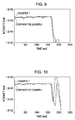
- FIG. 9 is a plot showing Fe compositional profiles measured along the depth of piezoelectric elements by SIMS.
- FIG. 10 is a plot showing Bi compositional profiles measured along the depth of piezoelectric elements by SIMS.
- FIG. 11 is a plot of S-V curves of the piezoelectric elements of Examples 1 and 2 and Comparative Example 1.
- FIG. 12 is a schematic view of a recording apparatus according to an embodiment of the invention.
- the flow channel substrate 10 has a plurality of pressure generating chambers 12 arranged in parallel in the width direction of the pressure generating chambers 12 .
- the flow channel substrate 10 also has a communicating section 13 therein located outside the pressure generating chambers 12 in the longitudinal direction of the pressure generating chambers 12 .
- the communicating section 13 communicates with the pressure generating chambers 12 through corresponding ink supply channels 14 and communication paths 15 .
- the communicating section 13 communicates with a reservoir section 31 formed in a protective substrate (described later) to define part of a reservoir acting as a common ink chamber of the pressure generating chambers 12 .
- piezoelectric elements 300 are disposed on the adhesion layer 56 .
- Each piezoelectric element 300 has a multilayer structure including the first electrode 60 made of platinum, a piezoelectric layer 70 having a small thickness of 2 ⁇ m or less, preferably 0.3 to 1.5 ⁇ m, and a second electrode 80 .
- the piezoelectric element 300 mentioned herein refers to the portion including the first electrode 60 , the piezoelectric layer 70 and the second electrode 80 .
- one of the electrodes of the piezoelectric element 300 acts as a common electrode, and the other electrode and the piezoelectric layer 70 are formed for each pressure generating chamber 12 by patterning.
- the complex oxide containing Bi, Fe, Ba and Ti and having a perovskite structure can be represented by a complex oxide having a perovskite structure of a mixed crystal of bismuth ferrate and barium titanate, or a solid solution in which bismuth ferrate and barium titanate are uniformly dissolved. Bismuth ferrate and barium titanate cannot be detected independently in an X-ray diffraction pattern.
- the two compositions may be considered to be the same complex oxide. (1 ⁇ x )[Bi(Fe 1-y M y )O 3 ] ⁇ x [BaTiO 3 ] (2)
- the second electrode 80 provided for each piezoelectric element 300 is connected to a lead electrode 90 made of, for example, gold (Au).
- the lead electrode 90 extends from the end of the second electrode 80 near the ink supply channel 14 to the upper surface of the elastic film and, optionally, to the upper surface of an insulating film.
- the flow channel substrate 10 may have only the pressure generating chambers 12 , and the ink supply channels 14 communicating between the reservoir 100 and the respective pressure generating chambers 12 are formed in a member between the flow channel substrate 10 and the protective substrate 30 , such as the elastic film 50 and an optionally provided insulating film.
- the protective substrate 30 has a through hole 33 passing through the protective substrate 30 in the thickness direction. The ends of the lead electrodes 90 extending from the piezoelectric elements 300 are exposed in the through hole 33 .
- a drive circuit 120 is secured on the protective substrate 30 and drives the piezoelectric elements 300 arranged in parallel.
- the drive circuit 120 may be a circuit board, a semiconductor integrated circuit (IC) or the like.
- the drive circuit 120 is electrically connected to each lead electrode 90 with a conductive connection wire 121 , such as bonding wire.
- a compliance substrate 40 including a sealing film 41 and a fixing plate 42 is joined on the protective substrate 30 .
- the sealing film 41 is made of a flexible material having a low rigidity, and seals one end of the reservoir section 31 .
- the fixing plate 42 is made of a relatively hard material. The portion of the fixing plate 42 opposing the reservoir 100 is completely removed to form an opening 43 ; hence the reservoir 100 is closed at one end only with the flexible sealing film 41 .
- the ink jet recording head I of the present embodiment draws an ink through an ink inlet connected to an external ink supply unit (not shown).
- the ink is delivered to fill the spaces from the reservoir 100 to the nozzle apertures 21 .
- the ink jet recording head I applies a voltage between the first electrode 60 and each second electrode 50 corresponding to the pressure generating chambers 12 , according to the recording signal from the drive circuit 120 .
- the elastic film 50 , the adhesion layer 56 , the first electrode 60 and the piezoelectric layers 70 are deformed to increase the internal pressure in the pressure generating chambers 12 , thereby ejecting the ink through the nozzle apertures 21 .
- the present embodiment ensures high adhesion between the first electrode 60 and the piezoelectric layer 70 , the first electrode 60 is prevented from separating from the piezoelectric layer 70 even if the piezoelectric element is repeatedly operated.
- the ink jet recording head or liquid ejecting head can exhibit high durability and reliability.
- FIGS. 4A to 8B are sectional views of the pressure generating chamber taken in the longitudinal direction.
- a silicon dioxide film that will form an elastic film 50 is formed of silicon dioxide (SiO 2 ) or the like, by thermal oxidation or the like, on the surface of a silicon flow channel substrate wafer 110 .
- an adhesion layer 56 is formed of, for example, titanium oxide on the SiO 2 elastic film 50 by sputtering, thermal oxidation or the like, as shown in FIG. 4B .
- a platinum first electrode 60 is formed over the entire surface of the adhesion layer 56 by sputtering.
- a piezoelectric layer 70 is formed on the first electrode 60 .
- the piezoelectric layer 70 may be formed by any method without particular limitation.
- a chemical solution method may be applied, such as a sol-gel method or a metal-organic decomposition (MOD) method in which a solution of organic metal compounds containing Bi, Fe, Mn, Ti and Ba dissolved or dispersed in a solvent is applied onto the first electrode 60 , and the coating of the solution is dried and then fired to form a metal oxide piezoelectric layer 70 .
- Other methods may be used, such as laser ablation, sputtering, pulsed laser deposition (PLD), CVD or aerosol deposition, irrespective of liquid process or solid process.
- a sol or MOD solution (precursor solution) containing organic metal compounds containing Bi, Fe, Mn, Ti and Ba in such proportions as the resulting layer can have a desired composition is applied onto the first electrode 60 by spin coating or the like to form a piezoelectric precursor film 71 (coating step).
- the precursor solution is prepared by mixing organic metal compounds containing Bi, Fe, Mn, Ti and Ba so that the metals have desired mole fractions, and dissolving or dispersing the mixture in an organic solvent such as an alcohol.
- the mole ratios of the metals in the precursor solution satisfy the following relationships 0.01 ⁇ Ba/Bi ⁇ 0.6 and 0.01 ⁇ Mn/Bi ⁇ 0.1.
- Organic metal compounds containing Bi, Fe, Mn, Ti or Ba include metal alkoxides, organic acid salts, and ⁇ -diketone complexes.
- the organic metal compound containing Bi may be bismuth 2-ethylhexanoate.
- the organic metal compound containing Fe may be iron 2-ethylhexanoate.
- the piezoelectric precursor film 71 is dried for a certain time by being heated to a predetermined temperature (for example, 150 to 200° C.) (drying step). Then, the dried piezoelectric precursor film 71 is degreased by being heated to a predetermined temperature (for example, 350 to 450° C.) and allowed to stand at that temperature for a certain time (degreasing step).
- the degreasing mentioned herein is performed to remove the organic components from the piezoelectric precursor film 71 , for example, as NO 2 , CO 2 or H 2 O.
- the drying and degreasing may be performed in any atmosphere without particular limitation, and may be performed in the air, an oxygen atmosphere or an inert gas atmosphere. The steps of coating, drying and degreasing may be repeated.
- the precursor solution was dropped onto the surface of the substrate on which the titanium oxide film and the first electrode 60 had been formed, and was then subjected to spin coating at a speed of 3000 rpm, thus forming a piezoelectric precursor film (coating step). Then, the piezoelectric precursor film on the substrate was dried on a hot plate at 180° C. for 2 minutes (drying step). The piezoelectric precursor film was further subjected to degreasing on a hot plate at 350° C. for 2 minutes (degreasing step). The sequence of the steps of coating, drying and degreasing was repeated three times, and, then, the resulting precursor films were fired at 800° C. for 5 minutes in an oxygen atmosphere using a rapid thermal annealing (RTA) apparatus (firing step).
- RTA rapid thermal annealing
- FIGS. 9 and 10 show the results along the depth of the piezoelectric layer
- FIG. 10 shows the Bi compositional profiles along the depth of the piezoelectric layer.
- the piezoelectric element 300 of the above embodiment includes the first electrode 60 , the piezoelectric layer 70 and the second electrode 80 that are formed in that order on a substrate (flow channel substrate 10 ), the structure of the piezoelectric element is not limited to this structure.
- an embodiment of the invention can be applied to a vertical vibration piezoelectric element including layers of a piezoelectric material and an electrode material alternately formed so as to expand and contract in an axis direction.
- the ink jet recording apparatus II shown in FIG. 12 includes recording head units 1 A and 1 B each including the ink jet recording head I, and cartridges 2 A and 2 B for supplying ink are removably mounted in the respective recoding head units 1 A and 1 B.
- the recording head units 1 A and 1 B are loaded on a carriage 3 secured for movement along a carriage shaft 5 of an apparatus body 4 .
- the recording head units 1 A and 1 B discharge, for example, a black ink composition and a color ink composition, respectively.
- the piezoelectric elements according to embodiments of the invention can be used in other equipment, for example, ultrasonic oscillators and other ultrasonic wave devices, ultrasonic motors, piezoelectric sensors that detect deformation of the piezoelectric layer as electrical signals, pressure sensors, and pyroelectric sensors such as IR sensors, without being limited to the use in liquid ejecting heads such as ink jet recording heads.
- the piezoelectric element according to an embodiment of the invention may be applied to a ferroelectric element of a ferroelectric memory device.
Landscapes
- Engineering & Computer Science (AREA)
- Manufacturing & Machinery (AREA)
- Chemical & Material Sciences (AREA)
- Ceramic Engineering (AREA)
- Composite Materials (AREA)
- Materials Engineering (AREA)
- Particle Formation And Scattering Control In Inkjet Printers (AREA)
- Semiconductor Memories (AREA)
Abstract
Description
(1−x)[BiFeO3 ]−x[BaTiO3] (1)
-
- (0<x<0.40)
(Bi1-xBax)(Fe1-xTix)O3 (1′) - (0<x<0.40)
- (0<x<0.40)
(1−x)[Bi(Fe1-yMy)O3 ]−x[BaTiO3] (2)
-
- (0<x<0.40, 0.01<y<0.10)
(Bi1-xBax)((Fe1-yMy)1-xTix)O3 (2′) - (0<x<0.40, 0.01<y<0.10)
- (0<x<0.40, 0.01<y<0.10)
Claims (3)
Applications Claiming Priority (2)
| Application Number | Priority Date | Filing Date | Title |
|---|---|---|---|
| JP2012072573A JP2013207002A (en) | 2012-03-27 | 2012-03-27 | Liquid jet head, liquid jet apparatus and piezoelectric element |
| JP2012-072573 | 2012-03-27 |
Publications (2)
| Publication Number | Publication Date |
|---|---|
| US20130257999A1 US20130257999A1 (en) | 2013-10-03 |
| US8991984B2 true US8991984B2 (en) | 2015-03-31 |
Family
ID=49234408
Family Applications (1)
| Application Number | Title | Priority Date | Filing Date |
|---|---|---|---|
| US13/847,712 Expired - Fee Related US8991984B2 (en) | 2012-03-27 | 2013-03-20 | Liquid ejecting head, liquid ejecting apparatus, and piezoelectric element |
Country Status (2)
| Country | Link |
|---|---|
| US (1) | US8991984B2 (en) |
| JP (1) | JP2013207002A (en) |
Citations (3)
| Publication number | Priority date | Publication date | Assignee | Title |
|---|---|---|---|---|
| US20070241642A1 (en) * | 2006-04-12 | 2007-10-18 | Seiko Epson Corporation | Piezoelectric material and piezoelectric device |
| US20090230211A1 (en) | 2008-03-12 | 2009-09-17 | Fujifilm Corporation | Perovskite oxide, process for producing the perovskite oxide, and piezoelectric device |
| JP2009252789A (en) | 2008-04-01 | 2009-10-29 | Seiko Epson Corp | Piezoelectric material and piezoelectric element |
Family Cites Families (6)
| Publication number | Priority date | Publication date | Assignee | Title |
|---|---|---|---|---|
| JP2010214841A (en) * | 2009-03-18 | 2010-09-30 | Seiko Epson Corp | Liquid ejection head, liquid ejection device, and actuator device |
| WO2010114148A1 (en) * | 2009-03-31 | 2010-10-07 | Canon Kabushiki Kaisha | Ceramic, piezoelectric device, and production method thereof |
| JP5681398B2 (en) * | 2009-07-09 | 2015-03-04 | 富士フイルム株式会社 | Perovskite oxide, ferroelectric composition, piezoelectric body, piezoelectric element, and liquid ejection device |
| JP5839157B2 (en) * | 2010-03-02 | 2016-01-06 | セイコーエプソン株式会社 | Liquid ejecting head, liquid ejecting apparatus, piezoelectric element, ultrasonic sensor and infrared sensor |
| JP5527527B2 (en) * | 2010-03-12 | 2014-06-18 | セイコーエプソン株式会社 | Liquid ejecting head and liquid ejecting apparatus |
| JP2011222849A (en) * | 2010-04-13 | 2011-11-04 | Seiko Epson Corp | Liquid injection head, liquid injector and piezoelectric device |
-
2012
- 2012-03-27 JP JP2012072573A patent/JP2013207002A/en not_active Withdrawn
-
2013
- 2013-03-20 US US13/847,712 patent/US8991984B2/en not_active Expired - Fee Related
Patent Citations (4)
| Publication number | Priority date | Publication date | Assignee | Title |
|---|---|---|---|---|
| US20070241642A1 (en) * | 2006-04-12 | 2007-10-18 | Seiko Epson Corporation | Piezoelectric material and piezoelectric device |
| US20090230211A1 (en) | 2008-03-12 | 2009-09-17 | Fujifilm Corporation | Perovskite oxide, process for producing the perovskite oxide, and piezoelectric device |
| JP2009242229A (en) | 2008-03-12 | 2009-10-22 | Fujifilm Corp | Perovskite oxide, process for producing the same, piezoelectric body, piezoelectric element, and liquid discharging device |
| JP2009252789A (en) | 2008-04-01 | 2009-10-29 | Seiko Epson Corp | Piezoelectric material and piezoelectric element |
Also Published As
| Publication number | Publication date |
|---|---|
| JP2013207002A (en) | 2013-10-07 |
| US20130257999A1 (en) | 2013-10-03 |
Similar Documents
| Publication | Publication Date | Title |
|---|---|---|
| US9356223B2 (en) | Liquid ejecting head and liquid ejecting apparatus | |
| US8573754B2 (en) | Methods for manufacturing liquid ejecting head and piezoelectric element, liquid ejecting head, liquid ejecting apparatus, and piezoelectric element | |
| US8662644B2 (en) | Liquid ejecting head and liquid ejecting apparatus, and piezoelectric element | |
| US9425379B2 (en) | Piezoelectric element and piezoelectric element application device | |
| US8608289B2 (en) | Liquid ejecting head, liquid ejecting apparatus, and piezoelectric element | |
| US10734570B2 (en) | Piezoelectric element and piezoelectric element applied device | |
| US8770723B2 (en) | Piezoelectric element, liquid ejecting head, and liquid ejecting apparatus | |
| US8636343B2 (en) | Liquid ejecting head, liquid ejecting apparatus, and piezoelectric element | |
| JP6146599B2 (en) | Piezoelectric element, liquid ejecting head, liquid ejecting apparatus, ultrasonic device and sensor | |
| US9312791B2 (en) | Piezoelectric element, liquid ejecting head, liquid ejecting apparatus, ultrasonic sensor, piezoelectric motor, and power generating apparatus | |
| US9385299B2 (en) | Liquid ejecting head, liquid ejecting apparatus, and piezoelectric element | |
| US8991984B2 (en) | Liquid ejecting head, liquid ejecting apparatus, and piezoelectric element | |
| JP2013098441A (en) | Liquid injection head, liquid injection device and piezoelectric element | |
| JP2013098442A (en) | Liquid injection head, liquid injection device and piezoelectric element | |
| US8746856B2 (en) | Piezoelectric element, liquid ejecting head, and liquid ejecting apparatus | |
| JP2015061048A (en) | Liquid ejecting head, liquid ejecting apparatus, and piezoelectric element | |
| JP6350810B2 (en) | Piezoelectric material, piezoelectric element, liquid ejecting head, liquid ejecting apparatus, and ultrasonic measuring apparatus | |
| US8783837B2 (en) | Liquid jet head, liquid jet apparatus, and piezoelectric element | |
| JP2014194992A (en) | Liquid injection head, liquid injection apparatus, and piezoelectric element | |
| JP5915848B2 (en) | Piezoelectric element manufacturing method, liquid ejecting head manufacturing method, liquid ejecting apparatus manufacturing method, ultrasonic device manufacturing method, and sensor manufacturing method | |
| US8632169B2 (en) | Liquid ejecting head, liquid ejecting apparatus, piezoelectric element, and method for evaluating piezoelectric layer | |
| JP2013165195A (en) | Liquid injection head, liquid injection device and piezoelectric element | |
| CN116896973A (en) | Piezoelectric element and piezoelectric element application device |
Legal Events
| Date | Code | Title | Description |
|---|---|---|---|
| AS | Assignment |
Owner name: SEIKO EPSON CORPORATION, JAPAN Free format text: ASSIGNMENT OF ASSIGNORS INTEREST;ASSIGNORS:KITADA, KAZUYA;ASAKAWA, TSUTOMU;SIGNING DATES FROM 20130307 TO 20130308;REEL/FRAME:030050/0834 |
|
| STCF | Information on status: patent grant |
Free format text: PATENTED CASE |
|
| MAFP | Maintenance fee payment |
Free format text: PAYMENT OF MAINTENANCE FEE, 4TH YEAR, LARGE ENTITY (ORIGINAL EVENT CODE: M1551); ENTITY STATUS OF PATENT OWNER: LARGE ENTITY Year of fee payment: 4 |
|
| FEPP | Fee payment procedure |
Free format text: MAINTENANCE FEE REMINDER MAILED (ORIGINAL EVENT CODE: REM.); ENTITY STATUS OF PATENT OWNER: LARGE ENTITY |
|
| LAPS | Lapse for failure to pay maintenance fees |
Free format text: PATENT EXPIRED FOR FAILURE TO PAY MAINTENANCE FEES (ORIGINAL EVENT CODE: EXP.); ENTITY STATUS OF PATENT OWNER: LARGE ENTITY |
|
| STCH | Information on status: patent discontinuation |
Free format text: PATENT EXPIRED DUE TO NONPAYMENT OF MAINTENANCE FEES UNDER 37 CFR 1.362 |
|
| FP | Lapsed due to failure to pay maintenance fee |
Effective date: 20230331 |