US8975964B2 - BEMF monitor gain calibration stage in hard disk drive servo integrated circuit - Google Patents
BEMF monitor gain calibration stage in hard disk drive servo integrated circuit Download PDFInfo
- Publication number
- US8975964B2 US8975964B2 US13/759,848 US201313759848A US8975964B2 US 8975964 B2 US8975964 B2 US 8975964B2 US 201313759848 A US201313759848 A US 201313759848A US 8975964 B2 US8975964 B2 US 8975964B2
- Authority
- US
- United States
- Prior art keywords
- ladder
- fine
- banks
- bank
- fine ladder
- Prior art date
- Legal status (The legal status is an assumption and is not a legal conclusion. Google has not performed a legal analysis and makes no representation as to the accuracy of the status listed.)
- Active, expires
Links
- 238000004519 manufacturing process Methods 0.000 claims 2
- 235000020637 scallop Nutrition 0.000 abstract description 10
- 241000237509 Patinopecten sp. Species 0.000 abstract description 9
- 238000000034 method Methods 0.000 abstract description 6
- 238000013461 design Methods 0.000 abstract description 5
- 230000003121 nonmonotonic effect Effects 0.000 abstract description 4
- 208000032750 Device leakage Diseases 0.000 abstract 2
- 241000237503 Pectinidae Species 0.000 abstract 1
- 235000021162 brunch Nutrition 0.000 abstract 1
- 230000000694 effects Effects 0.000 description 12
- 230000003044 adaptive effect Effects 0.000 description 6
- 230000003071 parasitic effect Effects 0.000 description 6
- 230000007423 decrease Effects 0.000 description 4
- XUIMIQQOPSSXEZ-UHFFFAOYSA-N Silicon Chemical compound [Si] XUIMIQQOPSSXEZ-UHFFFAOYSA-N 0.000 description 3
- 229910052710 silicon Inorganic materials 0.000 description 3
- 239000010703 silicon Substances 0.000 description 3
- 239000007787 solid Substances 0.000 description 2
- 229920000954 Polyglycolide Polymers 0.000 description 1
- 238000007792 addition Methods 0.000 description 1
- 238000013459 approach Methods 0.000 description 1
- 238000004364 calculation method Methods 0.000 description 1
- 238000012217 deletion Methods 0.000 description 1
- 230000037430 deletion Effects 0.000 description 1
- 230000009977 dual effect Effects 0.000 description 1
- 238000012886 linear function Methods 0.000 description 1
- 238000005259 measurement Methods 0.000 description 1
- 238000012986 modification Methods 0.000 description 1
- 230000004048 modification Effects 0.000 description 1
- 238000012544 monitoring process Methods 0.000 description 1
- 235000010409 propane-1,2-diol alginate Nutrition 0.000 description 1
- 238000006467 substitution reaction Methods 0.000 description 1
- 239000000758 substrate Substances 0.000 description 1
- 238000012546 transfer Methods 0.000 description 1
Images


Classifications
-
- H—ELECTRICITY
- H03—ELECTRONIC CIRCUITRY
- H03G—CONTROL OF AMPLIFICATION
- H03G3/00—Gain control in amplifiers or frequency changers
-
- H—ELECTRICITY
- H03—ELECTRONIC CIRCUITRY
- H03G—CONTROL OF AMPLIFICATION
- H03G1/00—Details of arrangements for controlling amplification
- H03G1/0005—Circuits characterised by the type of controlling devices operated by a controlling current or voltage signal
- H03G1/0088—Circuits characterised by the type of controlling devices operated by a controlling current or voltage signal using discontinuously variable devices, e.g. switch-operated
-
- H—ELECTRICITY
- H03—ELECTRONIC CIRCUITRY
- H03G—CONTROL OF AMPLIFICATION
- H03G3/00—Gain control in amplifiers or frequency changers
- H03G3/001—Digital control of analog signals
Definitions
- This application is directed, in general, to amplifiers in Hard Disk Drives (HDD) servo system and, more specifically, to a gain calibration of an amplifier in monitoring back electro-motive force (BEMF) of VCM motor in servo integrated circuits (ICs).
- HDD Hard Disk Drives
- BEMF back electro-motive force
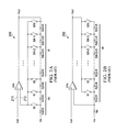
- FIG. 1 illustrates a prior art BEMF system 100 having an A 1 gain amplifier 110 of a Voice Coil Motor (VCM) 120 BEMF monitor in HDD servo IC.
- VCM Voice Coil Motor
- the VCM motor 120 In gain calibration mode, the VCM motor 120 is made still so its BEMF voltage is zero. Meanwhile, about 100 mA current is forced flowing through VCM motor and sense resistor Rs. The voltage drop on the sense resistor Rs is amplified by a digital programmable gain amplifier A 1 , and the A 1 gain output is cancelled out with VCM voltage at A 2 gain stage 130 . Make A 2 output zero by digitally changing A 1 gain, A 1 amplifier 110 gain is digitally calibrated to be equal to a ratio of motor resistance R VCM and sense resistance R SNS , that is,
- a 2 amplifier 130 output is an estimation of VCM motor BEMF voltage.
- a 13-bit DAC is used for A 1 programmable gain stage 110 to achieve required mV-level BEMF voltage measurement accuracy.
- FIGS. 2A and 2B illustrate two prior art Programmable Gain Amplifier (PGA) approaches to BEMF monitor gain calibration of A 1 gain 110 .
- switches of a first prior art PGA 200 performing gain programmability are tied to an operational amplifier's (OPA's) negative input node, and the switch on-state resistance R ds,on does not contribute to PGA gain error, because of an infinite impedance, thus zero input bias current to the inputs 211 and 212 of CMOS OPA.
- OPA's operational amplifier's
- the scheme of the PGA 200 also has a disadvantage.
- the PGA 200 gain which is R f /R in , moves from 63 to 62/2 then to 61/3 which are non-linear gain steps.
- the PGA 200 does not have a linear transfer function although the digital code linearly changes. This lack of linearity does not meet system level requirements for typical servo systems.
- an alternative prior art PGA 250 of the A 1 gain 110 the input resistance R in between input Vin and the OPA negative input node is fixed, and the feedback resistance R f is linearly coded by switches.
- the gain of the PGA 250 of an A 1 PGA 110 is a linear function of the linearly coded resistance.
- the A 1 gain is linear to the digital code change only when the switch on-state resistances are ideally zero.
- the switch on-state resistances S 1 -SN are in the signal path and they contribute to the amplifier gain error, unlike the prior art PGA 200 .
- the switch resistances S( 1 )-S(N) and the poly resistors R(N) that create the gain for the PGA 250 have different temperature coefficients and voltage coefficients, and it can traverse into gain error over temperature variation and over voltage signal excursion during the operation.
- FIG. 3 shows a prior art dual ladder DAC, with NMOS resistors used in the fine ladder forming a 13 bit programmable PGA.
- FIG. 3 illustrates a prior art dual-ladder architecture of 6+7, that is, implementing 6-bit in a coarse ladder and 7-bit in a fine ladder. This avoids the large number of switches and resistors used in either the PGA 200 or the PGA 250 .
- the resistance of on-state switch 321 and 322 between a coarse ladder 310 and a fine ladder 320 are considered as one unit of the fine ladder 320 ;
- MOS resistors 323 , 324 , 325 , 326 are used in the fine ladder 320 , where a MOS resistor is defined as a MOS device working in deep triode region. Therefore, all the units along the fine ladder are same type of elements and they match with each other very well (over temperature and process variations) and the DAC DNL/INL performance is improved and silicon area is reduced.
- R CL // ( NR FL ) R CL should be less than 0.5LSB.
- R FL should be designed larger than a specific value.
- ratio (N ⁇ R FL )/R CL is too large and over a certain threshold, the nominal current flowing through the fine ladder 320 is so small that it is conquered by the current leakage in the fine ladder 320 .
- PGA 300 if equal resistances are used in the coarse ladder 310 , the resulting programmable gain is not linear to the digital code as illustrated as line 330 . To obtain the linear gain as line 331 , the resistances in the coarse ladder 310 have to be carefully computed and they must not be equal.
- the fine ladder 420 nominal current is mostly leaked away locally at the back gate parasitic p-n junction diodes 424 and 425 in MOS resistors 421 , back gate parasitic p-n junction diodes 426 and 427 in MOS resistor 422 and so on, as well as back gate parasitic p-n junction of switches 431 , 432 and so on, all associated with the fine ladder 420 .
- ratio (N ⁇ R FL )/R CL is too large and the nominal current flowing through fine ladder 420 is small and comparable to leakage current, the net current goes through fine ladder MOS resistor channel notably decreases due to local MOS back gate leakage.
- MOS resistors are used in the DAC fine ladder 420 and its resistances are designed to be much larger than the coarse ladder 410 unit resistance, that is, a large ratio (N ⁇ R FL )/R CL .
- An undesired side-effect is that the nominal current of the fine ladder 420 , which is a ratio R CL /(N ⁇ R FL +R CL ) of the total current from Vin to Vout of the PGA stage, become extremely small.
- a first aspect provides an apparatus including a hard drive preamplifier, the hard drive preamplifier including: a coarse ladder having a plurality of resistors, wherein each of the plurality of resistors are individually addressable; a fine ladder that is coupled to the coarse ladder, wherein the find ladder includes a plurality of banks of FETs, each bank including a plurality of FETs, and a fine ladder controller, wherein the each of the plurality of banks of the fine ladder are controllable by the fine ladder controller.
- a second aspect provides a system including a hard drive preamplifier, the hard drive preamplifier including: a first amplifier having a first gain, the first amplifier including a coarse ladder having a plurality of resistors, wherein each of the plurality of resistors are individually addressable; a fine ladder that is coupled to the coarse ladder, wherein the find ladder includes a plurality of banks of FETs, each bank including a plurality of FETs, and a fine ladder controller, wherein the each of the plurality of banks of the fine ladder are controllable by the fine ladder controller, a second amplifier having a second gain, a summer coupled to an output of the first gain and the second gain.
- a third aspect provides a system a system including a hard drive preamplifier, the hard drive preamplifier including: a first amplifier having a first gain, the first amplifier including a coarse ladder having a plurality of resistors, wherein each of the plurality of resistors are individually addressable; a fine ladder that is coupled to the coarse ladder, wherein the find ladder includes a plurality of banks of FETs, each bank including a plurality of FETs, and a fine ladder controller, wherein the each of the plurality of banks of the fine ladder are controllable by the fine ladder controller, a second amplifier having a second gain, a summer coupled to an output of the first gain and the second gain, wherein, each of the FETs is an NFET, wherein a PMOS is coupled to each corresponding NFET.
- FIG. 1 illustrates BEMF monitor 100 with a BEMF digital programmable gain amplifier
- FIG. 2A illustrates a first prior art PGA of the BEMF programmable gain amplifier of FIG. 1 ;
- FIG. 2B illustrates a second prior art PGA of the BEMF programmable gain amplifier of FIG. 1 ;
- FIG. 3 illustrates a prior art PGA 300 where design trade off of “shunt effect” and ‘leakage effect” simultaneously exist.
- FIG. 4 illustrates a prior art PGA 400 where the back gate current leakage conquer the nominal fine ladder current, the voltage potential along the fine ladder does not monotonically decreases and non-linear gain scallop occurs.
- FIG. 5 illustrates a new art BEMF programmable gain amplifier 500 having a plurality of levels of fine ladder adaptive control and back gate leakage current compensation
- FIG. 6 illustrates that the back gate leakage current of NMOS devices associated with node 599 is locally compensated by PMOS devices back gate leakage current.
- FIG. 7 illustrates a comparison between the prior art gain plot (red trace with non-linear scallop) and the new art gain plot (purple straight line) while digital gain control code is programmed from 0000H to 1FFFH.
- FIG. 4 illustrated is one aspect, to avoid the on-state switch resistance effect and achieve 13-bit resolution and accuracy on the programmable gain amplifier, the schematic in FIG. 2A (with no Rdson effect on gain accuracy) has been chosen and it is improved to be linear with respect to the programming code.
- every resistance unit in the coarse ladder should be carefully calculated. Given a minimum gain G MIN and a maximum gain G MAX and a targeted coarse ladder resolution implementation (e.g.
- FIG. 5 illustrated is a circuit 500 for new art PGA in servo BEMF monitor circuit.
- an adaptive control on the fine ladder depends on which coarse ladder resistor is shunted so the ratio (N ⁇ R FL )/R CL is adaptively adjusted, therefore the net current flowing through every unit in the fine ladder is kept relatively constant.
- the fine ladder resistance is adaptively adjusted be its smallest, to keep the fine ladder current, which is a ratio R 1 /(R 1 +4R 2 ) of total current, be a constant and far away from the level easily conquered by leakage current.
- the fine ladder adaptive control logic circuit 510 set output control signal 511 ‘high’ and other control signal 512 , 513 514 ‘low’, so that only one fine ladder bank with MOS resistor aspect ratio 1*(W/L) is turned on and all other three NMOS resistor banks (respectively with MOS resistor of aspect ratio 8(W/L), 4(W/L), 2(W/L) are turned off, and equivalent fine ladder resistance of 64*R 2 is shunted with R( 64 ).
- the fine ladder resistance is also adaptively adjusted be its largest, to keep the fine ladder current, which is a ratio R( 64 )/(R( 64 )+64*R 2 ) of total current, be a constant and far away from the level easily conquered by leakage current.
- a bank of PMOS devices 570 is parallel coupled with the NMOS banks 571 , 572 , 573 , 574 .
- the PMOS bank 570 has exactly same device count and each device is parallel tied to the corresponding each NMOS device in NMOS banks During the operation, the gate of each PMOS device in the PMOS bank 570 is permanently connected to logic “1”, so that the PMOS devices are turned off all the time during the operation.
- the PMOS bank 570 is turned off and it is out of circuit operation, however, the back gate leakage currents of the PMOS devices (the leakage current flows through PMOS source/drain parasitic diode from 1.8V back gate NWELL to its source/drain) are used to compensate for the local leakage current generated by the NMOS devices (the leakage current flows from NMOS drain/source to back gate substrate ground).
- the back gate leakage current of NMOS parasitic diodes is provided by a local PMOS back-gate leakage current.
- PMOS devices 532 , 533 and NMOS devices 581 , 582 , 583 , 584 all associated with node 599 , have been drawn for simplicity.
- the channels of fine ladder MOS resistors experience same amount net current from the beginning to the end along the fine ladder, without being distracted by local leakage current. Therefore the current flowing through the fine ladder is consistently in one direction and it is far away the current level conquered by the leakage current, thus the non-linear scallop described earlier has been eliminated.
- the PMOS/NMOS back gate leakage is independent of the PMOS/NMOS on or off state, therefore the back gate of the PMOS and NMOS banks in the fine ladder presents a constant leakage current all the time, no matter how many number of the NMOS banks are turned on or turned off. That is, the leakage compensation is independent of the adaptive control operation of NMOS banks.
- FIG. 7 illustrates a comparison between the prior art gain plot (dashed trace) and the new art gain plot (solid trace) while digital programming code excises from 0000H to 1FFFH.
- the lower left portion shows the zoom-in plot of the most right portion of FIG. 6 , the non-linear scallop can be clearly observed in prior art gain plot (red trace) and completely eliminated in new art gain plot (solid trace).
Landscapes
- Analogue/Digital Conversion (AREA)
Abstract
Description
V A2OUT =V VCM −V A1OUT=(V VCM
As shown in Equation (1),
to
The A1 gain is linear to the digital code change only when the switch on-state resistances are ideally zero.
should be less than 0.5LSB. To reach the goal, RFL should be designed larger than a specific value. On the other hand, if ratio (N×RFL)/RCL is too large and over a certain threshold, the nominal current flowing through the
Claims (14)
Priority Applications (1)
| Application Number | Priority Date | Filing Date | Title |
|---|---|---|---|
| US13/759,848 US8975964B2 (en) | 2012-02-06 | 2013-02-05 | BEMF monitor gain calibration stage in hard disk drive servo integrated circuit |
Applications Claiming Priority (3)
| Application Number | Priority Date | Filing Date | Title |
|---|---|---|---|
| US201261595340P | 2012-02-06 | 2012-02-06 | |
| US201261625485P | 2012-04-17 | 2012-04-17 | |
| US13/759,848 US8975964B2 (en) | 2012-02-06 | 2013-02-05 | BEMF monitor gain calibration stage in hard disk drive servo integrated circuit |
Publications (2)
| Publication Number | Publication Date |
|---|---|
| US20130200954A1 US20130200954A1 (en) | 2013-08-08 |
| US8975964B2 true US8975964B2 (en) | 2015-03-10 |
Family
ID=48902373
Family Applications (1)
| Application Number | Title | Priority Date | Filing Date |
|---|---|---|---|
| US13/759,848 Active 2033-05-30 US8975964B2 (en) | 2012-02-06 | 2013-02-05 | BEMF monitor gain calibration stage in hard disk drive servo integrated circuit |
Country Status (1)
| Country | Link |
|---|---|
| US (1) | US8975964B2 (en) |
Families Citing this family (4)
| Publication number | Priority date | Publication date | Assignee | Title |
|---|---|---|---|---|
| US10264363B2 (en) | 2015-03-24 | 2019-04-16 | Tdk Corporation | MEMS microphone with improved sensitivity |
| US10587794B2 (en) * | 2018-04-25 | 2020-03-10 | Semiconductor Components Industries, Llc | Methods and apparatus for actuator control |
| CN109104157B (en) * | 2018-07-19 | 2021-04-02 | 电子科技大学 | A self-zeroing operational amplifier |
| CN112636753B (en) * | 2020-12-16 | 2024-04-09 | 普源精电科技股份有限公司 | Digital-to-analog converter |
Citations (3)
| Publication number | Priority date | Publication date | Assignee | Title |
|---|---|---|---|---|
| US5523721A (en) * | 1992-05-20 | 1996-06-04 | Fujitsu Limited | Digitally controlled variable gain circuit |
| US6538508B2 (en) * | 2001-04-27 | 2003-03-25 | Broadcom Corporation | Programmable gain amplifier with glitch minimization |
| US20070075769A1 (en) * | 2005-09-30 | 2007-04-05 | Thomas Blon | Circuit configuration having a feedback operational amplifier |
-
2013
- 2013-02-05 US US13/759,848 patent/US8975964B2/en active Active
Patent Citations (3)
| Publication number | Priority date | Publication date | Assignee | Title |
|---|---|---|---|---|
| US5523721A (en) * | 1992-05-20 | 1996-06-04 | Fujitsu Limited | Digitally controlled variable gain circuit |
| US6538508B2 (en) * | 2001-04-27 | 2003-03-25 | Broadcom Corporation | Programmable gain amplifier with glitch minimization |
| US20070075769A1 (en) * | 2005-09-30 | 2007-04-05 | Thomas Blon | Circuit configuration having a feedback operational amplifier |
Also Published As
| Publication number | Publication date |
|---|---|
| US20130200954A1 (en) | 2013-08-08 |
Similar Documents
| Publication | Publication Date | Title |
|---|---|---|
| US6617888B2 (en) | Low supply voltage differential signal driver | |
| US7425866B2 (en) | Digitally adjusted variable gain amplifier (VGA) using switchable differential pairs | |
| KR101629063B1 (en) | Power amplifier | |
| US7663420B2 (en) | MOS resistance controlling device and MOS attenuator | |
| US8975964B2 (en) | BEMF monitor gain calibration stage in hard disk drive servo integrated circuit | |
| WO2014070701A1 (en) | Method and apparatus for load adaptive ldo bias and compensation | |
| US20210219396A1 (en) | Current control circuitry | |
| US7154329B2 (en) | Method and apparatus for compensating amplifier output for temperature and process variations | |
| US7253700B1 (en) | Circuit for controlling a linear-in-decibels attenuator circuit using an analog control signal | |
| US9966913B2 (en) | Linear-in-dB, low-voltage, programmable/variable gain amplifier (PGA) using recursive current division | |
| US7969130B2 (en) | Voltage supply interface with current sensitivity and reduced series resistance | |
| KR20180054903A (en) | Variable-gain amplifier with improved power-supply noise rejection | |
| US7911293B2 (en) | Thermometer coded attenuator | |
| CN106464222B (en) | Programmable Gain Amplifier PGA and Programmable Resistor Network Circuit | |
| US20130027092A1 (en) | Digital Output Driver | |
| US9705524B2 (en) | R2R digital-to-analog converter circuit | |
| WO2017007566A1 (en) | Apparatus and method for measuring load current by applying compensated gain to voltage derived from drain-to-source voltage of power gating device | |
| US9374064B1 (en) | Micro-step resistance networks | |
| KR20150106734A (en) | Apparatus for driving actuator of camera module in mobile device | |
| US7800441B2 (en) | Feedback amplifier and audio system thererof | |
| CN108781061A (en) | Amplifying circuit, receiving circuit and semiconductor integrated circuit | |
| US7525366B2 (en) | Offset compensation using non-uniform calibration | |
| US8077060B2 (en) | Distributed threshold adjustment for high speed receivers | |
| KR20130029622A (en) | Circuit for controlling bias of power amplification module | |
| US8791682B2 (en) | Noise rejecting high-side power switch |
Legal Events
| Date | Code | Title | Description |
|---|---|---|---|
| AS | Assignment |
Owner name: TEXAS INSTRUMENTS INCORPORATED, TEXAS Free format text: ASSIGNMENT OF ASSIGNORS INTEREST;ASSIGNORS:LI, QUNYING;TAN, WENXIAO;SWIZE, GREGORY;SIGNING DATES FROM 20130204 TO 20130205;REEL/FRAME:029758/0691 |
|
| STCF | Information on status: patent grant |
Free format text: PATENTED CASE |
|
| MAFP | Maintenance fee payment |
Free format text: PAYMENT OF MAINTENANCE FEE, 4TH YEAR, LARGE ENTITY (ORIGINAL EVENT CODE: M1551); ENTITY STATUS OF PATENT OWNER: LARGE ENTITY Year of fee payment: 4 |
|
| MAFP | Maintenance fee payment |
Free format text: PAYMENT OF MAINTENANCE FEE, 8TH YEAR, LARGE ENTITY (ORIGINAL EVENT CODE: M1552); ENTITY STATUS OF PATENT OWNER: LARGE ENTITY Year of fee payment: 8 |