US8975880B2 - Internal capacitor linear regulator with transient dip compensator for internal-switch switching regulator - Google Patents
Internal capacitor linear regulator with transient dip compensator for internal-switch switching regulator Download PDFInfo
- Publication number
- US8975880B2 US8975880B2 US13/243,041 US201113243041A US8975880B2 US 8975880 B2 US8975880 B2 US 8975880B2 US 201113243041 A US201113243041 A US 201113243041A US 8975880 B2 US8975880 B2 US 8975880B2
- Authority
- US
- United States
- Prior art keywords
- voltage
- type transistor
- coupled
- switching regulator
- output
- Prior art date
- Legal status (The legal status is an assumption and is not a legal conclusion. Google has not performed a legal analysis and makes no representation as to the accuracy of the status listed.)
- Active, expires
Links
Images


Classifications
-
- H—ELECTRICITY
- H02—GENERATION; CONVERSION OR DISTRIBUTION OF ELECTRIC POWER
- H02M—APPARATUS FOR CONVERSION BETWEEN AC AND AC, BETWEEN AC AND DC, OR BETWEEN DC AND DC, AND FOR USE WITH MAINS OR SIMILAR POWER SUPPLY SYSTEMS; CONVERSION OF DC OR AC INPUT POWER INTO SURGE OUTPUT POWER; CONTROL OR REGULATION THEREOF
- H02M3/00—Conversion of DC power input into DC power output
- H02M3/02—Conversion of DC power input into DC power output without intermediate conversion into AC
- H02M3/04—Conversion of DC power input into DC power output without intermediate conversion into AC by static converters
- H02M3/10—Conversion of DC power input into DC power output without intermediate conversion into AC by static converters using discharge tubes with control electrode or semiconductor devices with control electrode
- H02M3/145—Conversion of DC power input into DC power output without intermediate conversion into AC by static converters using discharge tubes with control electrode or semiconductor devices with control electrode using devices of a triode or transistor type requiring continuous application of a control signal
- H02M3/155—Conversion of DC power input into DC power output without intermediate conversion into AC by static converters using discharge tubes with control electrode or semiconductor devices with control electrode using devices of a triode or transistor type requiring continuous application of a control signal using semiconductor devices only
- H02M3/156—Conversion of DC power input into DC power output without intermediate conversion into AC by static converters using discharge tubes with control electrode or semiconductor devices with control electrode using devices of a triode or transistor type requiring continuous application of a control signal using semiconductor devices only with automatic control of output voltage or current, e.g. switching regulators
- H02M3/158—Conversion of DC power input into DC power output without intermediate conversion into AC by static converters using discharge tubes with control electrode or semiconductor devices with control electrode using devices of a triode or transistor type requiring continuous application of a control signal using semiconductor devices only with automatic control of output voltage or current, e.g. switching regulators including plural semiconductor devices as final control devices for a single load
- H02M3/1588—Conversion of DC power input into DC power output without intermediate conversion into AC by static converters using discharge tubes with control electrode or semiconductor devices with control electrode using devices of a triode or transistor type requiring continuous application of a control signal using semiconductor devices only with automatic control of output voltage or current, e.g. switching regulators including plural semiconductor devices as final control devices for a single load comprising at least one synchronous rectifier element
-
- H—ELECTRICITY
- H03—ELECTRONIC CIRCUITRY
- H03K—PULSE TECHNIQUE
- H03K2217/00—Indexing scheme related to electronic switching or gating, i.e. not by contact-making or -breaking covered by H03K17/00
- H03K2217/0081—Power supply means, e.g. to the switch driver
-
- Y—GENERAL TAGGING OF NEW TECHNOLOGICAL DEVELOPMENTS; GENERAL TAGGING OF CROSS-SECTIONAL TECHNOLOGIES SPANNING OVER SEVERAL SECTIONS OF THE IPC; TECHNICAL SUBJECTS COVERED BY FORMER USPC CROSS-REFERENCE ART COLLECTIONS [XRACs] AND DIGESTS
- Y02—TECHNOLOGIES OR APPLICATIONS FOR MITIGATION OR ADAPTATION AGAINST CLIMATE CHANGE
- Y02B—CLIMATE CHANGE MITIGATION TECHNOLOGIES RELATED TO BUILDINGS, e.g. HOUSING, HOUSE APPLIANCES OR RELATED END-USER APPLICATIONS
- Y02B70/00—Technologies for an efficient end-user side electric power management and consumption
- Y02B70/10—Technologies improving the efficiency by using switched-mode power supplies [SMPS], i.e. efficient power electronics conversion e.g. power factor correction or reduction of losses in power supplies or efficient standby modes
-
- Y02B70/1466—
Definitions
- Embodiments described herein generally relate to switching regulators, and more particularly integrated circuit switching regulators which generate internal supply voltages for driving the power switches. More specifically, the invention relates to switching regulators in which low-dropout voltage regulators (“LDOs”) provide an intermediate supply voltage for driving power transistors under circumstances in which a supply voltage is greater than a gate drive voltage of a power transistor of the regulator.
- LDOs low-dropout voltage regulators
- a switching regulator that can absorb switching energy when driving the output power switches utilizing an internal capacitor without the need for an external capacitor.
- FIG. 1 (Prior Art) is a block diagram of a known switching regulator.
- FIG. 2 (Prior Art) is a block diagram of another known switching regulator.
- FIG. 3 is a block diagram of a switching regulator according to an exemplary embodiment of the present invention.
- FIG. 4 (Prior Art) is schematic diagram of a known switching regulator.
- FIG. 5 (Prior Art) is a schematic diagram of another known switching regulator.
- FIG. 6 is a schematic diagram of a switching regulator according to an exemplary embodiment of the present invention.
- FIGS. 7A , 7 B, and 7 C illustrate certain aspects of the operation of a switching regulator and waveforms of signals at different elements of an exemplary embodiment of a switching regulator according to the invention.
- FIGS. 8A and 8B illustrate certain additional aspects of a switching regulator and waveforms of signals at different elements of an exemplary embodiment of a switching regulator according to the invention.
- FIGS. 9A and 9B illustrate certain aspects of a dip compensator and waveforms of signals at different elements of a dip compensator of an exemplary embodiment of a switching regulator according to the invention.
- FIG. 10 is a flowchart 1000 of a process illustrating operation of an embodiment of a switching regulator according to the invention.
- FIG. 1 is a block diagram of a known switching regulator 100 .
- the switching regulator 100 includes a signal generator 106 which is provided an unregulated voltage 102 and a loopback voltage 104 .
- the signal generator 106 provides a signal 107 to a switching block 108 .
- the signal 107 is first provided to a pre-drivers block 110 .
- the output of the pre-drivers block 110 is coupled to a switching transistors block 112 . Switching transistors of switching transistors block 112 are switched “ON” and “OFF” by the output provided by the pre-driver block 110 .
- An output of the switching block 108 is provided to an inductor 114 and an external capacitor 116 which is connected to a ground 118 .
- a regulated voltage 120 is provided to a load 122 .
- FIG. 2 (Prior Art) is a block diagram of another known switching regulator 200 .
- Switching regulator 200 includes a signal generator 206 receiving an input unregulated voltage 202 and a loopback voltage 204 .
- Inductor 216 , external capacitor 218 , ground 220 and load 222 function essentially the same as their respective counterpart elements shown in FIG. 1 (Prior Art).
- Signal generator 206 provides a signal 207 to a switching block 208 .
- Low-dropout regulators (“LDOs”) 210 provide an output 211 which is coupled, along with the signal 207 from signal generator 206 , to a pre-drivers block 212 .
- the output of pre-drivers block 212 is coupled to the switching transistors block 214 .
- switching transistors block 214 switching transistors are turned “ON” and “OFF” by the output provided by the pre-drivers block 212 .
- An output of the switching block 208 is provided to an inductor 216 and an external capacitor 218 which is connected to a ground 220 .
- a regulated voltage 222 is provided to load 224 .
- FIG. 4 is a schematic diagram of a known switching regulator 400 .
- a signal generator 401 may be functionally similar to signal generator 106 .
- a switching block 403 may function similarly to switching block 108 .
- the switching regulator 400 includes respective pre-drivers 402 and 404 coupled to a p-type switching transistor 406 and a n-type transistor 408 .
- a supply voltage 410 is provided to pre-drivers 402 and 404 .
- the respective drains of the p-type transistor 406 and the n-type transistor 408 are coupled to external components 412 .
- These external components 412 including an inductor 414 and a capacitor 416 provide a loopback voltage 416 to the controller 418 , which also receives a reference voltage 420 .
- a controller 418 drives a Non Overlap Generator 422 .
- Pre-drivers 402 and 404 are connected to a ground 424 . Since, capacitor 416 is an external capacitor (external to an integrated circuit in chip in which switching regulator 400 is formed), the gate drive voltage of the respective transistors ( 406 and 408 ) can be equal to the supply voltage 410 . This equal level of the gate drive voltages and the supply voltage 410 allows there to be no over-voltage stress on any of the transistor junctions.
- FIG. 5 is a schematic diagram of another known switching regulator 500 .
- Signal generator 501 is functionally similar to signal generator 206 and switching block 503 is functionally similar to switching block 208 .
- Switching regulator 500 includes pre-drivers 502 and 504 coupled to respective p-type switching transistor 506 and a n-type switching transistor 508 .
- Two off-chip capacitors 509 and 510 that are a part of external components 512 , each having a value of 100 nF, are provided to absorb transient current from the switching of respective power transistors 506 and 508 .
- the respective drains of the p-type transistor 506 and the n-type transistor 508 are coupled to external components 512 .
- These external components 512 comprise of an inductor 516 and a capacitor 518 , and provide a loopback voltage 520 to a controller 522 .
- a reference voltage (“Vref”) 524 is also provided to the controller 522 .
- the controller 522 along with a LDO ( 528 ) drives the Non Overlap Generator 526 . Furthermore, a p-transistor side LDO (“PLDO”) 530 and a n-transistor side LDO (“NLDO”) 532 , are provided to generate respective intermediate voltages (“VPLDO” 534 and “VNDLO” 536 ) for the respective switching transistors ( 506 and 508 ). A ground 538 provides a completed circuit path for current switched by switching transistors 506 and 508 .
- PLDO p-transistor side LDO
- NLDO n-transistor side LDO
- the gate drive voltage of the transistors ( 506 and 508 ) is limited to the respective intermediate voltages ( 534 and 536 ).
- the maximum gate source voltage is limited to (Vsupply 514 ⁇ VPLDO 534 ) whereas for n-type transistor 508 , the gate source voltage is limited to (VNLDO 536 ⁇ ground 538 ).
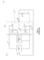
- FIG. 3 is a block diagram of a switching regulator 300 according to an exemplary embodiment of the present invention.
- Switching regulator 300 includes a signal generator 306 having an unregulated voltage 302 input, and receiving a loopback voltage 304 .
- Switching regulator 300 is intended to drive an external load 322 .
- the signal generator 306 provides a signal 307 to a switching block 308 .
- an output 311 of LDOs 310 along with signal 307 from signal generator 306 , is provided to the pre-drivers block 312 .
- the output 313 of the pre-drivers block 312 is coupled to the dip compensators block 314 , which contains dip compensators. Functional aspects of dip compensators are described later in the specification.
- the dip compensators block 314 is coupled to an input of the switching transistors block 316 , which includes switching transistors that are switched “ON” and “OFF” based on the output 313 provided by the pre-drivers block 312 .
- Internal capacitors 318 are provided within switching transistors block 316 .
- An output of the switching block 308 is provided to an inductor 324 and an external capacitor 326 which is connected to a ground 328 .
- a regulated voltage 320 which is equivalent to the loopback voltage 304 is provided to load 322 .
- FIG. 6 is a schematic diagram illustrating certain aspects of a switching regulator 600 according to an exemplary embodiment of the present invention.
- signal generator 601 may be functionally similar to signal generator 306 and switching block 603 may be functionally similar to switching block 308 .
- the switching regulator 600 includes pre-drivers 602 and 604 coupled to respective p-type transistor 606 and a n-type transistor 608 .
- Two internal capacitors 610 and 612 that are coupled to a supply to ground rail of the respective pre-drivers ( 602 and 604 ) are included.
- the internal capacitors 610 and 612 may have a capacitance in a range of 80 pF to 160 pF, with a preferable value of 140 pF.
- the capacitance level of the internal capacitors 610 and 612 is substantially equal to the gate capacitances of respective transistors 606 and 608 . In other embodiments, the capacitance level of the internal capacitors 610 and 612 may be two times to the level of gate capacitances of respective transistors 606 and 608 .
- the respective drains of the p-type transistor 606 and the n-type transistor 608 are configured to provide an output voltage 616 .
- the respective drains of the p-type transistor 606 and the n-type transistor 608 are coupled to external components 650 .
- These external components 650 comprise of an inductor 652 and a capacitor 654 , and provide a loopback voltage 622 to a controller 624 .
- a reference voltage (“Vref”) 626 is also provided to a controller 624 .
- the controller 624 is coupled to a Non Overlap Generator 628 .
- a p-transistor side LDO (“PLDO”) 630 and a n-transistor side LDO (“NLDO”) 632 are provided to generate respective intermediate voltages (VPLDO 634 and VNDLO 636 ) for the respective transistors ( 606 and 608 ).
- VPLDO 634 and VNDLO 636 respective intermediate voltages
- VNDLO 636 respective intermediate voltages
- a ground connection 638 completes a circuit patch for currents switched by transistors 606 and 608 .
- An internal capacitor region 640 further includes a PLDO Dip Compensator 642 and NLDO Dip Compensator 644 .
- the gate of the p-type transistor 606 is provided a value of pgate 646 and the gate of the n-type transistor 608 is provided a value of ngate 648 .
- LDO 630 and NLDO 632 Internally miller compensated LDOs (PLDO 630 and NLDO 632 ) are used to compensate for the load capacitance of the internal capacitors 610 and 612 .
- the LDOs ( 630 and 632 ) provide DC voltage regulation for the intermediate supply (VPLDO 634 and VNLDO 636 ).
- the PLDO 630 and NDLO 632 each respectively act as a slow correction loop for the voltage regulation.
- each of the respective slow loops Working in parallel with each of the respective slow loops are the respective PLDO Dip Compensator 642 and the respective NLDO Dip Compensator 644 .
- Each of the Dip Compensators acts as a fast localized loop that corrects any voltage dip due to the turning “ON” of a power transistor.
- FIG. 7A illustrates, certain aspects of a switching regulator 700 according to another exemplary embodiment of the present invention.
- a switching regulator 700 includes a NLDO 702 that provides an intermediate voltage (“VNDLO”) 704 to an internal capacitor 706 and a pre-driver 708 .
- VNDLO intermediate voltage
- the pre-driver 708 is illustrated in its “OFF” state and is connected to a Capacitor (“NSW Capacitor”) 710 .
- the NSW Capacitor 710 represents a gate capacitance of a n-type transistor (not shown).
- the voltage that is provided to the NSW Capacitor 710 is ngate 712 .
- FIG. 7B illustrates certain aspects of the switching regulator 700 according to another exemplary embodiment of the present invention. Specifically, FIG. 7 b illustrates aspects of a switching regulator 700 , with the pre-driver 708 is illustrated in an “ON” state.
- FIG. 7C illustrates a waveform of the VNLDO 704 being provided by the NDLO 702 , and the levels of ngate 712 in various states of being “ON” and “OFF”. DeltaV in each of the respective waveform represents a change in the voltage level of that specific element.
- VNLDO 704 When, the pre-driver 708 is in an “ON” state, a charge is transferred from the internal capacitor 706 to the NSW Capacitor 710 . Since the turn-on time is quite fast and the NLDO 702 cannot react to the instantaneous change, VNLDO 704 will dip according to a charge transfer rule. If the capacitance of the internal capacitor 706 is equal to the capacitance of NSW Capacitor 710 , then the amount of the voltage dip is equal to a level of VNLDO 704 divided by 2 .
- the recovery of the voltage will depend on the LDO output transconductance (“gm”) and the recovery time constant is usually gm/(value of the internal capacitor 706 plus the value of the NSW Capacitor 710 ).
- gm LDO output transconductance
- the recovery time constant is usually gm/(value of the internal capacitor 706 plus the value of the NSW Capacitor 710 ).
- FIG. 8A illustrates, certain aspects of a switching regulator 800 according to another exemplary embodiment of the present invention.
- a NDLO 802 provides an intermediate voltage 804 to an internal capacitor 806 and a pre-driver 808 .
- the pre-driver 808 is an “ON” state and is connected to a Capacitor (“NSW Capacitor”) 810 .
- the pre-driver 808 is configured to be able to be put in an “OFF” state as well.
- the NSW Capacitor 810 represents a gate capacitance of a n-type transistor (not shown).
- the voltage that is provided to the NSW Capacitor 810 is ngate 812 .
- Coupled to the structure is a NLDO Dip Compensator 514 which provides a signal (“SW”) 816 through a switch 818 .
- a charging current (“Icharge”) 820 is also provided to the switch 818 , from a Voltage Supply 822 .
- the addition of the NLDO Dip Compensator 814 allows for a localized fast loop that reduces a voltage dip and speeds up recovery time.
- the NLDO dip compensator 814 provides the SW 816 that enables a charger to charge VNLDO 804 when pre-driver 808 is turned “ON”. In this case the voltage dip will be reduced and the recovery can be controlled by controlling Icharge 820 . This provides a fast charging path that pre-empts the on-chip capacitor charge loss, thereby reducing transient voltage drop.
- FIG. 8B illustrates the waveform of some of the elements shown in the FIG. 8 a embodiment.
- DeltaV in each of the respective waveforms represents a change in the voltage level of that specific element.
- SW 816 is the signal that is provided by the NLDO dip compensator 814 .
- FIG. 9A is a schematic diagram illustrating certain aspects of a Dip Compensator 900 according to exemplary embodiments of the present invention.
- Dip Compensator 900 functional similarly to NLDO Dip Compensator 642 .
- Dip Compensator 900 includes a NLDO Charger 902 and a NLDO Comparator 904 and a Schmitt Trigger section 906 .
- the NDLO Charger 902 includes a supply voltage (“Vsupply”) 908 , two p-type transistors ( 910 and 912 ), resistors ( 914 and 916 ) coupled to a p-type transistor 912 .
- an n-type transistor 918 connected to a ground 920 through a resistor 922 are included within a NDLO Charger 902 .
- the Schmitt Trigger section 906 generates reset pulses 924 by adding the output of a signal ngate 926 through a Schmitt trigger 928 and another signal ngateb 927 .
- a NOR gate 930 generates the reset pulses 924 that are provided to a comparator 932 in the NLDO comparator 904 .
- the reset pulses 924 reset the output of a comparator 932 to send out a high level of a signal (“SW”) 934 , which enables turning “ON” of the NLDO Charger circuit 902 .
- SW high level of a signal
- the comparator 932 will start to monitor the level of VNLDO 936 and a low pass version of VNLDO (“VNLDO LP”) 938 .
- VNLDO LP 938 is generated by the use of a resistor 940 , a capacitor 942 and a current source 944 which are connected to a ground 946 .
- the comparator 932 will issue a low value of SW 934 that that turns off the NLDO charger circuit 902 .
- the LDO will take over the recovery of the voltage level of VNLDO 936 .
- the amount of a charging current (not shown) produced by the NLDO charger 902 can be controlled by varying the resistance level of resistor 922 .
- the voltage drop across resistor 922 is the source follower voltage of n-type transistor 918 . If the SW 914 is at a high level and if the voltage being supplied is equal to VNLDO 936 , then the voltage generated across resistor 922 R 4 will be (VNLDO 936 -gate-to-source voltage of n-type transistor 918 ) and the current generated will be (VNLDO 936 -gate-to-source voltage of n-type transistor 918 )/(resistance level of resistor 922 ).
- This current will serve as a reference charge current that charges up the gate of transistor 910 first, as the initial current is blocked by resistor 916 .
- the blocking of the current by the resistor 916 allows the transistor 910 gate to charge up quickly, providing a large current to an internal capacitor (not shown) to aid in controlling the voltage dip.
- the gate voltage of transistor 912 will be equal to the gate voltage of transistor 910 .
- transistor 912 will behave as a conventional current mirror which provides a constant charging current to the internal capacitor.
- the charging current may be determined by the current mirror ratio between transistor 910 and transistor 912 . If the ratio is determined to be k. Then the charger current from transistor 910 will be equal to
- FIG. 9B illustrates waveforms of signals at some of the elements shown in FIG. 9 a .
- a waveform of the VNLDO 936 and VNLDO LP 938 , SW 934 , ngate 926 , ngateb 927 , and reset 924 are presented.
- Levels of ngate 927 in various states of being “ON” and “OFF” are presented.
- FIG. 10 is a flowchart 1000 illustrating the process by which switching regulators operate according to an exemplary embodiment of the present invention.
- An unregulated voltage is received in step 1002 .
- a switching clock is generated in step 1004 .
- a pre-driver Based on the switching clock, a pre-driver provides a voltage to a corresponding transistor to turn it on in step 1006 .
- a corresponding dip-compensator corrects a voltage dip caused by the turning on of the power transistor.
- Step 1010 entails outputting of the regulated voltage by thee transistors.
- This output voltage is provided as a loopback voltage back to step 1104 for generation of the switching clock, in a step 1012 .
- This output voltage may also be provided to a load.
Landscapes
- Engineering & Computer Science (AREA)
- Power Engineering (AREA)
- Dc-Dc Converters (AREA)
Abstract
Description
Claims (14)
Priority Applications (1)
| Application Number | Priority Date | Filing Date | Title |
|---|---|---|---|
| US13/243,041 US8975880B2 (en) | 2011-09-23 | 2011-09-23 | Internal capacitor linear regulator with transient dip compensator for internal-switch switching regulator |
Applications Claiming Priority (1)
| Application Number | Priority Date | Filing Date | Title |
|---|---|---|---|
| US13/243,041 US8975880B2 (en) | 2011-09-23 | 2011-09-23 | Internal capacitor linear regulator with transient dip compensator for internal-switch switching regulator |
Publications (2)
| Publication Number | Publication Date |
|---|---|
| US20130076320A1 US20130076320A1 (en) | 2013-03-28 |
| US8975880B2 true US8975880B2 (en) | 2015-03-10 |
Family
ID=47910577
Family Applications (1)
| Application Number | Title | Priority Date | Filing Date |
|---|---|---|---|
| US13/243,041 Active 2033-03-23 US8975880B2 (en) | 2011-09-23 | 2011-09-23 | Internal capacitor linear regulator with transient dip compensator for internal-switch switching regulator |
Country Status (1)
| Country | Link |
|---|---|
| US (1) | US8975880B2 (en) |
Cited By (1)
| Publication number | Priority date | Publication date | Assignee | Title |
|---|---|---|---|---|
| US20160020698A1 (en) * | 2013-03-14 | 2016-01-21 | Volterra Semiconductor LLC | Voltage Regulators with Kickback Protection |
Families Citing this family (6)
| Publication number | Priority date | Publication date | Assignee | Title |
|---|---|---|---|---|
| US9348383B2 (en) * | 2013-03-01 | 2016-05-24 | Intel Corporation | Apparatus for starting up switching voltage regulator |
| US9972995B2 (en) * | 2013-10-05 | 2018-05-15 | Taiwan Semiconductor Manufacturing Company Limited | Circuit with a droop compensating mechanism |
| US9645591B2 (en) * | 2014-01-09 | 2017-05-09 | Qualcomm Incorporated | Charge sharing linear voltage regulator |
| US9876494B2 (en) * | 2014-03-13 | 2018-01-23 | Maxim Integrated Products, Inc. | High voltage switching output driver |
| US9886048B2 (en) * | 2016-05-04 | 2018-02-06 | Qualcomm Incorporated | Headroom control in regulator systems |
| CN110888483A (en) * | 2019-12-11 | 2020-03-17 | 思瑞浦微电子科技(苏州)股份有限公司 | Electronic device based on dynamic zero compensation circuit |
Citations (4)
| Publication number | Priority date | Publication date | Assignee | Title |
|---|---|---|---|---|
| US20030128015A1 (en) * | 1999-12-30 | 2003-07-10 | Volterra Semiconductor Corporation A Delaware Corporation | Switching regulator with multiple power transistor driving voltages |
| US7064531B1 (en) * | 2005-03-31 | 2006-06-20 | Micrel, Inc. | PWM buck regulator with LDO standby mode |
| US7759916B2 (en) * | 2008-05-12 | 2010-07-20 | Microchip Technology Incorporated | Regulator with device performance dynamic mode selection |
| US7923976B2 (en) * | 2006-12-29 | 2011-04-12 | Texas Instruments Incorporated | Fault protection circuit, method of operating a fault protection circuit and a voltage regulator employing the same |
-
2011
- 2011-09-23 US US13/243,041 patent/US8975880B2/en active Active
Patent Citations (4)
| Publication number | Priority date | Publication date | Assignee | Title |
|---|---|---|---|---|
| US20030128015A1 (en) * | 1999-12-30 | 2003-07-10 | Volterra Semiconductor Corporation A Delaware Corporation | Switching regulator with multiple power transistor driving voltages |
| US7064531B1 (en) * | 2005-03-31 | 2006-06-20 | Micrel, Inc. | PWM buck regulator with LDO standby mode |
| US7923976B2 (en) * | 2006-12-29 | 2011-04-12 | Texas Instruments Incorporated | Fault protection circuit, method of operating a fault protection circuit and a voltage regulator employing the same |
| US7759916B2 (en) * | 2008-05-12 | 2010-07-20 | Microchip Technology Incorporated | Regulator with device performance dynamic mode selection |
Cited By (3)
| Publication number | Priority date | Publication date | Assignee | Title |
|---|---|---|---|---|
| US20160020698A1 (en) * | 2013-03-14 | 2016-01-21 | Volterra Semiconductor LLC | Voltage Regulators with Kickback Protection |
| US9847722B2 (en) * | 2013-03-14 | 2017-12-19 | Volterra Semiconductor LLC | Voltage regulators with kickback protection |
| US10243467B2 (en) | 2013-03-14 | 2019-03-26 | Volterra Semiconductor LLC | Voltage regulators with kickback protection |
Also Published As
| Publication number | Publication date |
|---|---|
| US20130076320A1 (en) | 2013-03-28 |
Similar Documents
| Publication | Publication Date | Title |
|---|---|---|
| US8975880B2 (en) | Internal capacitor linear regulator with transient dip compensator for internal-switch switching regulator | |
| JP6212225B2 (en) | Power converter soft start circuit | |
| US9030848B2 (en) | DC to DC converter | |
| US10008932B2 (en) | Synchronous rectification DC/DC converter | |
| US11435768B2 (en) | N-channel input pair voltage regulator with soft start and current limitation circuitry | |
| CN102455730A (en) | Semiconductor integrated circuit for regulator | |
| US20130278239A1 (en) | Precharge circuits and methods for dc-dc boost converters | |
| US20150365087A1 (en) | Duty cycle-controlled load switch | |
| US9240716B2 (en) | Switching power supply circuit | |
| CN108475984A (en) | DC-DC converters that have stable output characteristics over a wide range of input voltages and have devices that respond to input voltage variations | |
| JP5504782B2 (en) | Charge pump | |
| US9531259B2 (en) | Power supply circuit | |
| US20150002113A1 (en) | Power supply circuit | |
| US9929646B2 (en) | Charge pump circuit and step-down regulator circuit | |
| CN103631298B (en) | Linear stable | |
| US9559583B2 (en) | Power converter with a wave generator that filters a wave signal to generate an output voltage | |
| US8476878B2 (en) | Startup circuit for DC-DC converter | |
| CN104170228B (en) | Double-mode boost pressure controller | |
| CN103529901B (en) | Circuit used for supplying power for bootstrap circuit | |
| CN116780903B (en) | Direct-current voltage conversion circuit and chip | |
| US7570098B2 (en) | Active voltage-clamping gate driving circuit | |
| US10008923B2 (en) | Soft start circuit and power supply device equipped therewith | |
| US11239758B2 (en) | Power supply system with stable loop | |
| KR20070023596A (en) | Switching regulator | |
| US12339693B2 (en) | Circuit and system for actively discharging a power stage input node during power supply turn-on |
Legal Events
| Date | Code | Title | Description |
|---|---|---|---|
| AS | Assignment |
Owner name: BROADCOM CORPORATION, CALIFORNIA Free format text: ASSIGNMENT OF ASSIGNORS INTEREST;ASSIGNORS:CHAN, HUA BENG;CHEN, DEYU;LE, QUEENIE;REEL/FRAME:026961/0648 Effective date: 20110923 |
|
| STCF | Information on status: patent grant |
Free format text: PATENTED CASE |
|
| AS | Assignment |
Owner name: BANK OF AMERICA, N.A., AS COLLATERAL AGENT, NORTH CAROLINA Free format text: PATENT SECURITY AGREEMENT;ASSIGNOR:BROADCOM CORPORATION;REEL/FRAME:037806/0001 Effective date: 20160201 Owner name: BANK OF AMERICA, N.A., AS COLLATERAL AGENT, NORTH Free format text: PATENT SECURITY AGREEMENT;ASSIGNOR:BROADCOM CORPORATION;REEL/FRAME:037806/0001 Effective date: 20160201 |
|
| AS | Assignment |
Owner name: AVAGO TECHNOLOGIES GENERAL IP (SINGAPORE) PTE. LTD., SINGAPORE Free format text: ASSIGNMENT OF ASSIGNORS INTEREST;ASSIGNOR:BROADCOM CORPORATION;REEL/FRAME:041706/0001 Effective date: 20170120 Owner name: AVAGO TECHNOLOGIES GENERAL IP (SINGAPORE) PTE. LTD Free format text: ASSIGNMENT OF ASSIGNORS INTEREST;ASSIGNOR:BROADCOM CORPORATION;REEL/FRAME:041706/0001 Effective date: 20170120 |
|
| AS | Assignment |
Owner name: BROADCOM CORPORATION, CALIFORNIA Free format text: TERMINATION AND RELEASE OF SECURITY INTEREST IN PATENTS;ASSIGNOR:BANK OF AMERICA, N.A., AS COLLATERAL AGENT;REEL/FRAME:041712/0001 Effective date: 20170119 |
|
| MAFP | Maintenance fee payment |
Free format text: PAYMENT OF MAINTENANCE FEE, 4TH YEAR, LARGE ENTITY (ORIGINAL EVENT CODE: M1551); ENTITY STATUS OF PATENT OWNER: LARGE ENTITY Year of fee payment: 4 |
|
| AS | Assignment |
Owner name: AVAGO TECHNOLOGIES INTERNATIONAL SALES PTE. LIMITE Free format text: MERGER;ASSIGNOR:AVAGO TECHNOLOGIES GENERAL IP (SINGAPORE) PTE. LTD.;REEL/FRAME:047229/0408 Effective date: 20180509 |
|
| AS | Assignment |
Owner name: AVAGO TECHNOLOGIES INTERNATIONAL SALES PTE. LIMITE Free format text: CORRECTIVE ASSIGNMENT TO CORRECT THE EFFECTIVE DATE PREVIOUSLY RECORDED ON REEL 047229 FRAME 0408. ASSIGNOR(S) HEREBY CONFIRMS THE THE EFFECTIVE DATE IS 09/05/2018;ASSIGNOR:AVAGO TECHNOLOGIES GENERAL IP (SINGAPORE) PTE. LTD.;REEL/FRAME:047349/0001 Effective date: 20180905 |
|
| AS | Assignment |
Owner name: AVAGO TECHNOLOGIES INTERNATIONAL SALES PTE. LIMITE Free format text: CORRECTIVE ASSIGNMENT TO CORRECT THE PATENT NUMBER 9,385,856 TO 9,385,756 PREVIOUSLY RECORDED AT REEL: 47349 FRAME: 001. ASSIGNOR(S) HEREBY CONFIRMS THE MERGER;ASSIGNOR:AVAGO TECHNOLOGIES GENERAL IP (SINGAPORE) PTE. LTD.;REEL/FRAME:051144/0648 Effective date: 20180905 |
|
| MAFP | Maintenance fee payment |
Free format text: PAYMENT OF MAINTENANCE FEE, 8TH YEAR, LARGE ENTITY (ORIGINAL EVENT CODE: M1552); ENTITY STATUS OF PATENT OWNER: LARGE ENTITY Year of fee payment: 8 |