US8965159B1 - Implementing twisted pair waveguide for electronic substrates - Google Patents
Implementing twisted pair waveguide for electronic substrates Download PDFInfo
- Publication number
- US8965159B1 US8965159B1 US14/074,145 US201314074145A US8965159B1 US 8965159 B1 US8965159 B1 US 8965159B1 US 201314074145 A US201314074145 A US 201314074145A US 8965159 B1 US8965159 B1 US 8965159B1
- Authority
- US
- United States
- Prior art keywords
- twisted
- spinel
- generating
- recited
- conductor pair
- Prior art date
- Legal status (The legal status is an assumption and is not a legal conclusion. Google has not performed a legal analysis and makes no representation as to the accuracy of the status listed.)
- Expired - Fee Related
Links
Images


Classifications
-
- H—ELECTRICITY
- H05—ELECTRIC TECHNIQUES NOT OTHERWISE PROVIDED FOR
- H05K—PRINTED CIRCUITS; CASINGS OR CONSTRUCTIONAL DETAILS OF ELECTRIC APPARATUS; MANUFACTURE OF ASSEMBLAGES OF ELECTRICAL COMPONENTS
- H05K3/00—Apparatus or processes for manufacturing printed circuits
- H05K3/10—Apparatus or processes for manufacturing printed circuits in which conductive material is applied to the insulating support in such a manner as to form the desired conductive pattern
- H05K3/105—Apparatus or processes for manufacturing printed circuits in which conductive material is applied to the insulating support in such a manner as to form the desired conductive pattern by conversion of non-conductive material on or in the support into conductive material, e.g. by using an energy beam
-
- G—PHYSICS
- G02—OPTICS
- G02B—OPTICAL ELEMENTS, SYSTEMS OR APPARATUS
- G02B6/00—Light guides; Structural details of arrangements comprising light guides and other optical elements, e.g. couplings
- G02B6/44—Mechanical structures for providing tensile strength and external protection for fibres, e.g. optical transmission cables
- G02B6/4401—Optical cables
-
- H—ELECTRICITY
- H05—ELECTRIC TECHNIQUES NOT OTHERWISE PROVIDED FOR
- H05K—PRINTED CIRCUITS; CASINGS OR CONSTRUCTIONAL DETAILS OF ELECTRIC APPARATUS; MANUFACTURE OF ASSEMBLAGES OF ELECTRICAL COMPONENTS
- H05K1/00—Printed circuits
- H05K1/02—Details
- H05K1/0213—Electrical arrangements not otherwise provided for
- H05K1/0216—Reduction of cross-talk, noise or electromagnetic interference
- H05K1/0228—Compensation of cross-talk by a mutually correlated lay-out of printed circuit traces, e.g. for compensation of cross-talk in mounted connectors
-
- H—ELECTRICITY
- H05—ELECTRIC TECHNIQUES NOT OTHERWISE PROVIDED FOR
- H05K—PRINTED CIRCUITS; CASINGS OR CONSTRUCTIONAL DETAILS OF ELECTRIC APPARATUS; MANUFACTURE OF ASSEMBLAGES OF ELECTRICAL COMPONENTS
- H05K2201/00—Indexing scheme relating to printed circuits covered by H05K1/00
- H05K2201/09—Shape and layout
- H05K2201/09209—Shape and layout details of conductors
- H05K2201/09654—Shape and layout details of conductors covering at least two types of conductors provided for in H05K2201/09218 - H05K2201/095
- H05K2201/097—Alternating conductors, e.g. alternating different shaped pads, twisted pairs; Alternating components
-
- H—ELECTRICITY
- H05—ELECTRIC TECHNIQUES NOT OTHERWISE PROVIDED FOR
- H05K—PRINTED CIRCUITS; CASINGS OR CONSTRUCTIONAL DETAILS OF ELECTRIC APPARATUS; MANUFACTURE OF ASSEMBLAGES OF ELECTRICAL COMPONENTS
- H05K2203/00—Indexing scheme relating to apparatus or processes for manufacturing printed circuits covered by H05K3/00
- H05K2203/10—Using electric, magnetic and electromagnetic fields; Using laser light
- H05K2203/107—Using laser light
-
- H—ELECTRICITY
- H05—ELECTRIC TECHNIQUES NOT OTHERWISE PROVIDED FOR
- H05K—PRINTED CIRCUITS; CASINGS OR CONSTRUCTIONAL DETAILS OF ELECTRIC APPARATUS; MANUFACTURE OF ASSEMBLAGES OF ELECTRICAL COMPONENTS
- H05K2203/00—Indexing scheme relating to apparatus or processes for manufacturing printed circuits covered by H05K3/00
- H05K2203/11—Treatments characterised by their effect, e.g. heating, cooling, roughening
- H05K2203/1136—Conversion of insulating material into conductive material, e.g. by pyrolysis
-
- H—ELECTRICITY
- H05—ELECTRIC TECHNIQUES NOT OTHERWISE PROVIDED FOR
- H05K—PRINTED CIRCUITS; CASINGS OR CONSTRUCTIONAL DETAILS OF ELECTRIC APPARATUS; MANUFACTURE OF ASSEMBLAGES OF ELECTRICAL COMPONENTS
- H05K2203/00—Indexing scheme relating to apparatus or processes for manufacturing printed circuits covered by H05K3/00
- H05K2203/12—Using specific substances
- H05K2203/125—Inorganic compounds, e.g. silver salt
Definitions
- the present invention relates generally to the data processing field, and more particularly, relates to a method and structures for implementing an impedance-matched, low inductance, 3-dimensional (3D) twisted-pair waveguide within a printed circuit board dielectric material layer of electronic packaging.
- circuit board printed circuit board or PCB means a substrate or multiple layers (multi-layer) of substrates used for electronic packaging, for example, to electrically attach electrical components and should be understood to generally include circuit cards, printed circuit cards, backplanes, printed wiring cards, printed wiring boards, flex circuits, and ceramic or organic chip packaging substrates.
- U.S. Pat. No. 5,939,952 issued Aug. 17, 1999 to Noda et al., entitled “FLAT FLEXIBLE CABLE WITH PSEUDO-TWISTED CONDUCTORS” discloses a flat flexible electrical cable which includes a pair of pseudo-twisted conductors on a flexible dielectric substrate. Each conductor includes alternate straight and oblique sections. The straight sections of the conductors are generally parallel to each other and of uniform width. The oblique sections of the conductors cross each other at a crossover point. Each oblique section of each conductor is reduced in width uniformly in a direction from the straight-to-oblique transfer point of the respective conductor to the crossover point of the conductors.
- Principal aspects of the present invention are to provide a method and structures for implementing an impedance-matched, low inductance, 3-dimensional (3D) twisted-pair waveguide within a given dielectric material layer.
- Other important aspects of the present invention are to provide such method and structures substantially without negative effects and that overcome many of the disadvantages of prior art arrangements.
- a method and structures are provided for implementing impedance-matched, low inductance, 3-dimensional (3D) twisted-pairs within a given dielectric material layer.
- a dielectric material layer is loaded with an electrically insulating metal spinel compound at a set loading level.
- the spinel Upon exposure to a focused laser beam, the spinel is converted to a metallic particle with an electrical conductivity suitable for various applications.
- An impedance-matched, low inductance, 3-dimensional (3D) twisted-pair is generated using a laser direct structuring process with available fine depth control achieved with a laser.
- converting the spinel to a metallic particle with a set electrical conductivity includes generating an impedance-matched, low inductance, 3-dimensional twisted-pair waveguide.
- a laser direct structuring process exposing the electrically insulating metal spinel compound to a focused laser beam includes rastering the laser beam in an xy plane and controlling the focal depth in a z axis.
- FIG. 1 illustrates an example structure for implementing an impedance-matched, low inductance, 3-dimensional (3D) twisted-pair waveguide within a dielectric material layer in accordance with the preferred embodiment
- FIG. 2 is a flow chart illustrating exemplary steps for implementing an impedance-matched, low inductance, 3-dimensional (3D) twisted-pair waveguide within a dielectric material layer in accordance with the preferred embodiment
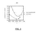
- FIG. 3 is a chart illustrating log resistivity for solution deposited and sputtered conducting spinel oxide films in accordance with a preferred embodiment.
- a method and structures are provided for implementing an impedance-matched, low inductance, 3-dimensional (3D) twisted-pair waveguide within a given dielectric material layer.
- An impedance-matched, low inductance, 3-dimensional (3D) twisted-pair waveguide is generated using a laser direct structuring process with a fine depth control achieved with a laser.
- a dielectric material layer is loaded with an electrically insulating metal spinel compound at a set loading level to be empirically determined. Upon exposure to a focused laser beam, the spinel is converted to a metallic particle with an electrical conductivity suitable for various applications.
- FIG. 1 there is shown an example structure for implementing an impedance-matched, low inductance, 3-dimensional (3D) twisted-pair or twisted-conductor pair generally designated by the reference character 100 within a dielectric material layer generally designated by the reference character 102 in accordance with preferred embodiments.
- the embedded impedance-matched, low inductance, 3-dimensional (3D) twisted-pair structure 100 provides, for example, an embedded 3D waveguide without disturbing signal wave propagation within the same dielectric material layer 102 .
- the twisted-pair structure 100 is formed in the given dielectric material layer 102 , such as a substrate used for electronic packaging, for example, circuit cards, printed circuit cards, backplanes, printed wiring cards, printed wiring boards, flex circuits, and ceramic or organic chip packaging substrates.
- the twisted-pair structure 100 includes a twisted-pair of a first conductor 104 and a second conductor 106 with an electrical insulator or an insulating dielectric 110 left between the conductors or traces 104 , 106 when generating embedded twisted pair structure.
- the conductors or traces 104 , 106 shown relative to an XY plane and a Z axis include respective conductor ends 112 and 114 , as shown.
- the embedded twisted-pair structure 100 is created using a laser direct structuring process modified to take advantage of the fine depth control that can be achieved with a laser, so that a true twisted pair 100 can be generated within a dielectric material 102 .
- FIG. 2 there is shown a flow chart illustrating exemplary steps for implementing an impedance-matched, low inductance, 3-dimensional (3D) twisted-pair waveguide within a dielectric material layer in accordance with the preferred embodiment.
- a given dielectric material layer is provided within a printed circuit board (PCB), flex or other electronic packaging dielectric layer.
- PCB printed circuit board
- the dielectric material layer is loaded with an electrically insulating metal spinel compound at a set loading level to be used for generating the twisted pair, as indicated in a block 204 .
- the electrically insulating metal spinel compound can be provided by a copper-containing spinel PK 3095 made by Ferro GmbH of Ferro Corporation, Mayfield Heights, Ohio 44124, USA.
- embedded twisted pairs in the given dielectric material layer are generated using laser direct structuring.
- the twisted pairs 100 advantageously are generated by rastering the laser in the XY plane and controlling the focal depth in the Z axis.
- the spinel in the electrically insulating metal spinel compound is converted into metal, such as copper (Cu) defining the twisted-pair of conductors 104 , 106 , as shown in FIG. 1 .
- the insulating dielectric 110 advantageously is left between the Cu traces or twisted-pair of conductors 104 , 106 thereby generating embedded twisted pair structure 100 in accordance with the preferred embodiment.
- FIG. 3 there is shown a chart illustrating conductivity values for solution-deposited and sputtered conducting spinel oxide films approaching almost metallic behavior in the case of the sputter deposited films provided in a publication entitled “Conducting spinel oxide films with infrared transparency” by Charles F. Windisch Jr., Kim F. Ferris, Gregory J. Exarhos, and, Shiv K. Sharma, Thin Solid Films 420-421 (2002) 89-99.
Abstract
Description
Claims (9)
Priority Applications (1)
| Application Number | Priority Date | Filing Date | Title |
|---|---|---|---|
| US14/074,145 US8965159B1 (en) | 2013-11-07 | 2013-11-07 | Implementing twisted pair waveguide for electronic substrates |
Applications Claiming Priority (1)
| Application Number | Priority Date | Filing Date | Title |
|---|---|---|---|
| US14/074,145 US8965159B1 (en) | 2013-11-07 | 2013-11-07 | Implementing twisted pair waveguide for electronic substrates |
Publications (1)
| Publication Number | Publication Date |
|---|---|
| US8965159B1 true US8965159B1 (en) | 2015-02-24 |
Family
ID=52473051
Family Applications (1)
| Application Number | Title | Priority Date | Filing Date |
|---|---|---|---|
| US14/074,145 Expired - Fee Related US8965159B1 (en) | 2013-11-07 | 2013-11-07 | Implementing twisted pair waveguide for electronic substrates |
Country Status (1)
| Country | Link |
|---|---|
| US (1) | US8965159B1 (en) |
Cited By (3)
| Publication number | Priority date | Publication date | Assignee | Title |
|---|---|---|---|---|
| US10320046B2 (en) * | 2015-06-09 | 2019-06-11 | At&T Intellectual Property I, L.P. | Apparatus and method utilizing a transmission medium with a plurality of hollow pathways |
| US10349532B2 (en) | 2017-07-20 | 2019-07-09 | International Business Machines Corporation | Method for implementing stub-less printed circuit board vias |
| US11025460B2 (en) | 2014-11-20 | 2021-06-01 | At&T Intellectual Property I, L.P. | Methods and apparatus for accessing interstitial areas of a cable |
Citations (17)
| Publication number | Priority date | Publication date | Assignee | Title |
|---|---|---|---|---|
| US3761842A (en) * | 1972-06-01 | 1973-09-25 | Bell Telephone Labor Inc | Twisted pair flat conductor cable with means to equalize impedance and propagation velocity |
| US4444801A (en) | 1981-01-14 | 1984-04-24 | Hitachi, Ltd. | Method and apparatus for correcting transparent defects on a photomask |
| EP0340997B1 (en) | 1988-05-02 | 1994-06-22 | Xerox Corporation | Electrically insulating polymer matrix with conductive path formed in situ |
| US5939952A (en) | 1996-05-24 | 1999-08-17 | Molex Incorporated | Flat flexible cable with pseudo-twisted conductors |
| US6071676A (en) | 1992-11-19 | 2000-06-06 | The University Court Of The University Of Dundee | Method of deposition |
| US6300846B1 (en) * | 1999-03-18 | 2001-10-09 | Molex Incorporated | Flat flexible cable with ground conductors |
| US6774741B2 (en) * | 2002-05-28 | 2004-08-10 | Decorp Americas, Inc. | Non-uniform transmission line and method of fabricating the same |
| US6807328B2 (en) | 1998-04-17 | 2004-10-19 | John Farah | Polished polyimide substrate |
| US6987428B2 (en) * | 2000-11-15 | 2006-01-17 | Intel Corporation | Electromagnetic coupler flexible circuit with a curved coupling portion |
| WO2006012057A1 (en) | 2004-06-30 | 2006-02-02 | Eastman Kodak Company | Forming electrical conductors on a substrate |
| US7031584B2 (en) | 2002-12-23 | 2006-04-18 | Electronics And Telecommunications Research Institute | Method for manufacturing optical waveguide using laser direct writing method and optical waveguide manufactured by using the same |
| US7391947B1 (en) | 2002-09-30 | 2008-06-24 | Translume, Inc. | Waveguide fabrication methods and devices |
| US20100136489A1 (en) | 2008-12-02 | 2010-06-03 | Tai Chao-Yi | Manufacturing device and manufacturing method for polymer waveguide device |
| GB2488575A (en) | 2011-03-02 | 2012-09-05 | Cretec Co Ltd | Method for forming a wiring pattern by laser irradiation |
| US8270788B2 (en) | 2006-05-19 | 2012-09-18 | Herman Peter R | Optical devices and digital laser method for writing waveguides, gratings, and integrated optical circuits |
| US8420301B2 (en) | 2011-02-28 | 2013-04-16 | Cretec Co., Ltd. | Method for forming a wiring pattern by laser irradiation |
| US8528203B2 (en) | 2011-06-07 | 2013-09-10 | International Business Machines Corporation | Providing selective via plating using laser resin activation |
-
2013
- 2013-11-07 US US14/074,145 patent/US8965159B1/en not_active Expired - Fee Related
Patent Citations (17)
| Publication number | Priority date | Publication date | Assignee | Title |
|---|---|---|---|---|
| US3761842A (en) * | 1972-06-01 | 1973-09-25 | Bell Telephone Labor Inc | Twisted pair flat conductor cable with means to equalize impedance and propagation velocity |
| US4444801A (en) | 1981-01-14 | 1984-04-24 | Hitachi, Ltd. | Method and apparatus for correcting transparent defects on a photomask |
| EP0340997B1 (en) | 1988-05-02 | 1994-06-22 | Xerox Corporation | Electrically insulating polymer matrix with conductive path formed in situ |
| US6071676A (en) | 1992-11-19 | 2000-06-06 | The University Court Of The University Of Dundee | Method of deposition |
| US5939952A (en) | 1996-05-24 | 1999-08-17 | Molex Incorporated | Flat flexible cable with pseudo-twisted conductors |
| US6807328B2 (en) | 1998-04-17 | 2004-10-19 | John Farah | Polished polyimide substrate |
| US6300846B1 (en) * | 1999-03-18 | 2001-10-09 | Molex Incorporated | Flat flexible cable with ground conductors |
| US6987428B2 (en) * | 2000-11-15 | 2006-01-17 | Intel Corporation | Electromagnetic coupler flexible circuit with a curved coupling portion |
| US6774741B2 (en) * | 2002-05-28 | 2004-08-10 | Decorp Americas, Inc. | Non-uniform transmission line and method of fabricating the same |
| US7391947B1 (en) | 2002-09-30 | 2008-06-24 | Translume, Inc. | Waveguide fabrication methods and devices |
| US7031584B2 (en) | 2002-12-23 | 2006-04-18 | Electronics And Telecommunications Research Institute | Method for manufacturing optical waveguide using laser direct writing method and optical waveguide manufactured by using the same |
| WO2006012057A1 (en) | 2004-06-30 | 2006-02-02 | Eastman Kodak Company | Forming electrical conductors on a substrate |
| US8270788B2 (en) | 2006-05-19 | 2012-09-18 | Herman Peter R | Optical devices and digital laser method for writing waveguides, gratings, and integrated optical circuits |
| US20100136489A1 (en) | 2008-12-02 | 2010-06-03 | Tai Chao-Yi | Manufacturing device and manufacturing method for polymer waveguide device |
| US8420301B2 (en) | 2011-02-28 | 2013-04-16 | Cretec Co., Ltd. | Method for forming a wiring pattern by laser irradiation |
| GB2488575A (en) | 2011-03-02 | 2012-09-05 | Cretec Co Ltd | Method for forming a wiring pattern by laser irradiation |
| US8528203B2 (en) | 2011-06-07 | 2013-09-10 | International Business Machines Corporation | Providing selective via plating using laser resin activation |
Non-Patent Citations (2)
| Title |
|---|
| Laser Micro-Fabrication of Waveguide Devices-IPCOM000034732D, Jan. 27, 2005. |
| Laser Micro-Fabrication of Waveguide Devices—IPCOM000034732D, Jan. 27, 2005. |
Cited By (6)
| Publication number | Priority date | Publication date | Assignee | Title |
|---|---|---|---|---|
| US11025460B2 (en) | 2014-11-20 | 2021-06-01 | At&T Intellectual Property I, L.P. | Methods and apparatus for accessing interstitial areas of a cable |
| US10320046B2 (en) * | 2015-06-09 | 2019-06-11 | At&T Intellectual Property I, L.P. | Apparatus and method utilizing a transmission medium with a plurality of hollow pathways |
| US10784554B2 (en) | 2015-06-09 | 2020-09-22 | At&T Intellectual Property I, L.P. | Transmission medium and method of communication comprising a cable with a core, a cladding, and at least one metallic conductive layers |
| US10985436B2 (en) | 2015-06-09 | 2021-04-20 | At&T Intellectual Property I, L.P. | Apparatus and method utilizing a transmission medium with hollow waveguide cores |
| US10349532B2 (en) | 2017-07-20 | 2019-07-09 | International Business Machines Corporation | Method for implementing stub-less printed circuit board vias |
| US11064616B2 (en) | 2017-07-20 | 2021-07-13 | International Business Machines Corporation | Method of implementing stub-less PCB vias |
Similar Documents
| Publication | Publication Date | Title |
|---|---|---|
| US10993331B2 (en) | High-speed interconnects for printed circuit boards | |
| US10117328B1 (en) | Flexible circuit board and method for manufacturing same | |
| US8084695B2 (en) | Via structure for improving signal integrity | |
| US7589398B1 (en) | Embedded metal features structure | |
| US20080173476A1 (en) | Embedded waveguide and embedded electromagnetic shielding | |
| JP7155261B2 (en) | Additive Manufacturing Technology (AMT) Faraday Boundaries in Radio Frequency Circuits | |
| WO2006089701A1 (en) | Air void via tuning | |
| US10798829B2 (en) | Implementing backdrilling elimination utilizing anti-electroplate coating | |
| US8965159B1 (en) | Implementing twisted pair waveguide for electronic substrates | |
| TW202013816A (en) | Millimeter wave phased array | |
| TWI640235B (en) | High frequency copper silver mixed conductive line structure and method same | |
| US20200008325A1 (en) | Module | |
| JP2003249731A (en) | Printed circuit board of coaxial cable structure and method of manufacturing the same | |
| CN104378922A (en) | Exquisite circuit board forming method suitable for high-frequency circuit | |
| Gazizov et al. | Stable delay of microstrip line with side grounded conductors | |
| CN101389182A (en) | Printed circuit board | |
| JP2010108635A (en) | Connection structure and connecting method of coaxial cable and base board | |
| US10537024B2 (en) | Process for fabricating printed circuit assembly and printed circuit assembly thereof | |
| Piekarz et al. | Suspended microstrip low-pass filter realized using FDM type 3D printing with conductive copper-based filament | |
| KR101360666B1 (en) | Emi shield consisting of a flexible printed circuit board method of manufacturing | |
| US6541853B1 (en) | Electrically conductive path through a dielectric material | |
| DE102012103018B4 (en) | Composite insulating layer and method of making the same | |
| US11064616B2 (en) | Method of implementing stub-less PCB vias | |
| US20080289869A1 (en) | Novel via structure for improving signal integrity | |
| US9775253B2 (en) | Insulating film, printed circuit board using the same, and method of manufacturing the printed circuit board |
Legal Events
| Date | Code | Title | Description |
|---|---|---|---|
| AS | Assignment |
Owner name: INTERNATIONAL BUSINESS MACHINES CORPORATION, NEW Y Free format text: ASSIGNMENT OF ASSIGNORS INTEREST;ASSIGNORS:DOYLE, MATTHEW S.;KUCZYNSKI, JOSEPH;SPLITTSTOESSER, KEVIN A.;AND OTHERS;SIGNING DATES FROM 20131017 TO 20131104;REEL/FRAME:031562/0063 |
|
| STCF | Information on status: patent grant |
Free format text: PATENTED CASE |
|
| FEPP | Fee payment procedure |
Free format text: MAINTENANCE FEE REMINDER MAILED (ORIGINAL EVENT CODE: REM.); ENTITY STATUS OF PATENT OWNER: LARGE ENTITY |
|
| LAPS | Lapse for failure to pay maintenance fees |
Free format text: PATENT EXPIRED FOR FAILURE TO PAY MAINTENANCE FEES (ORIGINAL EVENT CODE: EXP.); ENTITY STATUS OF PATENT OWNER: LARGE ENTITY |
|
| STCH | Information on status: patent discontinuation |
Free format text: PATENT EXPIRED DUE TO NONPAYMENT OF MAINTENANCE FEES UNDER 37 CFR 1.362 |
|
| FP | Lapsed due to failure to pay maintenance fee |
Effective date: 20190224 |