US8963598B2 - Duty rate detecter and semiconductor device using the same - Google Patents
Duty rate detecter and semiconductor device using the same Download PDFInfo
- Publication number
- US8963598B2 US8963598B2 US14/090,795 US201314090795A US8963598B2 US 8963598 B2 US8963598 B2 US 8963598B2 US 201314090795 A US201314090795 A US 201314090795A US 8963598 B2 US8963598 B2 US 8963598B2
- Authority
- US
- United States
- Prior art keywords
- duty rate
- output
- signal
- duration
- logic
- Prior art date
- Legal status (The legal status is an assumption and is not a legal conclusion. Google has not performed a legal analysis and makes no representation as to the accuracy of the status listed.)
- Active
Links
Images


Classifications
-
- G—PHYSICS
- G11—INFORMATION STORAGE
- G11C—STATIC STORES
- G11C11/00—Digital stores characterised by the use of particular electric or magnetic storage elements; Storage elements therefor
- G11C11/21—Digital stores characterised by the use of particular electric or magnetic storage elements; Storage elements therefor using electric elements
- G11C11/34—Digital stores characterised by the use of particular electric or magnetic storage elements; Storage elements therefor using electric elements using semiconductor devices
- G11C11/40—Digital stores characterised by the use of particular electric or magnetic storage elements; Storage elements therefor using electric elements using semiconductor devices using transistors
- G11C11/401—Digital stores characterised by the use of particular electric or magnetic storage elements; Storage elements therefor using electric elements using semiconductor devices using transistors forming cells needing refreshing or charge regeneration, i.e. dynamic cells
- G11C11/4063—Auxiliary circuits, e.g. for addressing, decoding, driving, writing, sensing or timing
- G11C11/407—Auxiliary circuits, e.g. for addressing, decoding, driving, writing, sensing or timing for memory cells of the field-effect type
- G11C11/4076—Timing circuits
-
- H—ELECTRICITY
- H03—ELECTRONIC CIRCUITRY
- H03K—PULSE TECHNIQUE
- H03K5/00—Manipulating of pulses not covered by one of the other main groups of this subclass
- H03K5/156—Arrangements in which a continuous pulse train is transformed into a train having a desired pattern
- H03K5/1565—Arrangements in which a continuous pulse train is transformed into a train having a desired pattern the output pulses having a constant duty cycle
-
- H—ELECTRICITY
- H03—ELECTRONIC CIRCUITRY
- H03K—PULSE TECHNIQUE
- H03K3/00—Circuits for generating electric pulses; Monostable, bistable or multistable circuits
- H03K3/01—Details
- H03K3/017—Adjustment of width or dutycycle of pulses
-
- G—PHYSICS
- G11—INFORMATION STORAGE
- G11C—STATIC STORES
- G11C7/00—Arrangements for writing information into, or reading information out from, a digital store
- G11C7/10—Input/output [I/O] data interface arrangements, e.g. I/O data control circuits, I/O data buffers
-
- G—PHYSICS
- G11—INFORMATION STORAGE
- G11C—STATIC STORES
- G11C7/00—Arrangements for writing information into, or reading information out from, a digital store
- G11C7/22—Read-write [R-W] timing or clocking circuits; Read-write [R-W] control signal generators or management
Definitions
- Exemplary embodiments of the present invention relate to semiconductor device, and more particularly, to a duty rate detection circuit and a semiconductor device using the same.
- DDR SDRAM Double Data Rate Synchronous Dynamic Random Access Memory
- a semiconductor device uses the clock signal as a source and generates an internal clock signal based on the clock signal. Since the semiconductor device performs an operation based on the internal clock signal, the frequency of the internal clock signal becomes the operation frequency of the semiconductor device. Therefore, the operation rate of the semiconductor device may be increased only by increasing the frequency of the internal clock signal.
- many methods for increasing the operation rate of a semiconductor device with a fixed frequency have been suggested. Among the methods is a method of increasing the applicability of a clock signal.
- Conventional Single Data Rate (SDR) scheme is a method of outputting a data to a rising edge of a clock signal
- conventional Double Data Rate (DDR) scheme is a method of outputting a data to a rising edge and a falling edge of a clock signal.
- DDR scheme two data are outputted in one cycle of a clock signal. Therefore, when a semiconductor device with the DDR scheme and a semiconductor device with the SDR scheme receive clock signals of the same frequency, the semiconductor device with the DDR scheme may process twice as much data as the semiconductor device of the SDR scheme does. This signifies that the operation rate of the semiconductor device with the DDR scheme is twice as fast as that of the semiconductor device with the SDR scheme.
- the DDR scheme uses the rising edge and falling edge of a clock signal, it is important to maintain the duty rate of the clock signal at 50:50. In other words, the logic high duration and the logic low duration of the clock signal have to be the same. If the duty rate of the clock signal goes out of 50:50 due to jitter and/or other reasons, data outputted in response to the clock signal may not be reliable. Thus, a circuit for controlling the duty rate of the clock signal is needed, and the circuit is called a duty rate correction circuit.
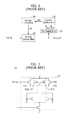
- FIG. 1 is a block diagram illustrating a conventional duty rate correction circuit.
- the duty rate correction circuit includes a duty rate correction block 110 , a clock dividing block 120 , a duty rate detection block 130 and a duty rate control block 140 .
- the duty rate correction block 110 is fed back with a duty control signal CTR, corrects the duty rate of an input clock signal CLK_IN and outputs a clock signal CLK_OUT with a corrected duty rate.
- the corrected clock signal CLK_OUT which is outputted from the duty rate correction block 110 , has almost the same duty rate as that of the input clock signal CLK_IN that may not have a duty rate of 50:50 before a duty rate correction operation is performed, and, after the duty rate correction operation is performed, the corrected clock signal CLK_OUT has a duty rate of 50:50.
- the clock dividing block divides the corrected clock signal CLK_OUT into a rising clock signal RCLK that corresponds to a rising edge and a falling dock signal FCLK that corresponds to a falling edge.
- the rising clock signal RCLK represents a logic high duration of the corrected clock signal CLK_OUT
- the falling clock signal FCLK represents a logic low duration of the corrected clock signal CLK_OUT. This will be described again later with reference to FIG. 3 .
- the duty rate detection block 130 detects a duty rate of the rising clock signal RCLK and the falling clock signal FCLK, which is the duty rate of the corrected clock signal CLK_OUT and generates a duty rate detection signal DET.
- the duty rate detection signal DET has a logic level value corresponding to the duty rate of the corrected clock signal CLK_OUT. For example, when the logic high duration of the corrected clock signal CLK_OUT is longer than the logic low duration, the duty rate detection signal DET may have a logic high value. When the logic low duration of the corrected clock signal CLK_OUT is longer than the logic high duration, the duty rate detection signal DET may have a logic low value.
- the duty rate control block 140 generates the control signal CTR for controlling the duty rate of the input clock signal CLK_IN in response to the duty rate detection signal DET.
- the control signal CTR is fed back into the duty rate correction block 110 , which controls the logic high duration or logic low duration of the input clock signal CLK_IN based on the control signal CTR and outputs the corrected clock signal CLK_OUT.
- the corrected dock signal CLK_OUT which is generated through the above-described duty rate correction operation, has a duty rate of 50:50.
- FIG. 2 is a circuit diagram illustrating the duty rate detection block 130 shown in FIG. 1 .
- the duty rate detection block 130 includes a sense amplifier 210 .
- the sense amplifier 210 may include a cross-couple-type sense amplification circuit, and it receives the rising clock signal RCLK and the falling clock signal FCLK to generate a first output signal OUT 1 and a second output signal OUT 2 .
- the sense amplifier 210 receives a strobe signal STB, and it controls starts of a charge operation and a discharge operation in response to the strobe signal STB.
- the duty rate detection signal DET shown in FIG. 1 is generated in response to the first output signal OUT 1 and the second output signal OUT 2
- FIG. 3 is a timing diagram illustrating operation of the sense amplifier 210 shown in FIG. 2 .
- the clock signal CLK_OUT is not fully corrected yet, and thus the logic high duration of the clock signal CLK_OUT is currently longer than the logic low duration.
- the logic high duration of the rising clock signal RCLK is longer than the logic high duration of the falling clock signal FCLK.
- the strobe signal STB is enabled and before a duty rate correction operation output are the first output signal OUT 1 and the second output signal OUT 2 , which are pre-charged with a predetermined voltage through a charge operation.
- the strobe signal STB is disabled, the first output signal OUT 1 is gradually discharged while still in the logic high duration of the rising clock signal RCLK, and the second output signal OUT 2 is gradually discharged while still in the logic high duration of the falling clock signal FCLK.
- the first output signal OUT 1 and the second output signal OUT 2 are amplified to predetermined voltage levels, respectively. Since the logic high duration of the rising clock signal RCLK is longer than the logic high duration of the falling clock signal FCLK in this example, the first output signal OUT 1 is pull-down amplified and the second output signal OUT 2 is pull-up amplified.
- the duty rate detection block 130 has the following drawbacks.
- the first output signal OUT 1 and the second output signal OUT 2 are respectively amplified to the predetermined voltage levels.
- the numbers of the discharges of the first output signal OUT 1 and of the second output signal OUT 2 may be different.
- the first output signal OUT 1 may be discharged seven times while the second output signal OUT 2 may be discharged six times.
- the amplification operation may be affected by the difference in the numbers of the discharges of the first output signal OUT 1 and of the second output signal OUT 2 . This means that the first output signal OUT 1 and the second output signal OUT 2 are not reliably compared, and thus means that the duty rate of the corrected clock signal CLK_OUT may not be accurately detected.
- Various embodiments of the present invention are directed to a duty rate detection circuit that may accurately detect the duty rate of a clock signal and a semiconductor device using the same.
- a duty rate detection circuit may include a duty rate detection block suitable for outputting a duty rate detection signal by detecting a duty rate of a clock signal having a first logic duration and a second logic duration and an output control block suitable for comparing the number of the first logic duration and the number of the second logic duration for a detection period and controlling an output moment of the duty rate detection signal.
- a semiconductor device may include a duty rate discharge unit suitable for performing a discharge operation in a first output terminal and a second output terminal during a first logic duration and a second logic duration of a clock signal, respectively, a level detection unit suitable for detecting voltage levels of the first output terminal and the second output terminal discharged to a predetermined target voltage level, an output unit suitable for detecting a duty rate of the clock signal at a moment when the number of the first logic duration and the number of the second logic duration representing the discharge operation time become the same after an output signal of the level detection unit is enabled and a locking information generation unit suitable for generating duty locking information by comparing the output signal of the level detection unit with an output signal of the output unit.
- a duty rate detection circuit may include a duty rate discharge unit suitable for respectively discharging a first terminal therein and a second terminal therein having corresponding predetermined voltage levels for corresponding duration between a first logic duration and a second logic duration of a clock signal, an output control unit suitable for generating a discharge detection signal synchronized with the first logic duration when one of the first terminal and the second terminal is discharged to a reference voltage level and an output unit suitable for detecting in response to the discharge detection signal synchronized with the first logic duration a duty rate of the clock signal based on the clock signal having toggled until the discharge detection signal is synchronized with the first logic duration, wherein, the duty rate discharge unit begin discharging in synchronized with the first logic duration.
- the duty rate detection circuit in accordance with the embodiments of the present invention may generate an accurate detection signal with the same number of discharges in the logic high duration and logic low duration of a clock signal.
- FIG. 1 is a block diagram illustrating a conventional duty rate correction circuit.
- FIG. 2 is a circuit diagram illustrating a duty rate detection block shown in FIG. 1 .
- FIG. 3 is a timing diagram illustrating operation of a sense amplifier shown in FIG. 2 .
- FIG. 4 is a block diagram illustrating a duty rate detection circuit in accordance with an embodiment of the present invention.
- FIG. 5 is a block diagram illustrating a duty rate detection block of the duty rate detection circuit shown in FIG. 4 .
- FIG. 6 is a block diagram illustrating an output control block of the duty rate detection circuit shown in FIG. 4 .
- FIG. 7 is a timing diagram illustrating operations of the duty rate detection circuit, the duty rate detection circuit and the output control block shown in FIGS. 4 to 6 .
- FIG. 8 is a block diagram illustrating a semiconductor device having the duty rate detection circuit shown in FIGS. 5 and 6 .
- FIGS. 9A to 9B are timing diagrams illustrating duty locking information of the semiconductor device shown in FIG. 8 .
- FIG. 4 is a block diagram illustrating a duty rate detection circuit in accordance with an embodiment of the present invention.
- the duty rate detection circuit includes a duty rate detection block 410 and an output control block 420 .
- the duty rate detection block 410 may receive a rising clock signal RCLK and a falling clock signal FCLK and generate a duty rate detection signal DET.
- the output control block 420 may compare the number of logic high durations of the rising clock signal RCLK with the number of logic high durations of the falling clock signal FCLK and control a time when the duty rate detection signal DET is output from the duty rate detection block 410 .
- the rising clock signal RCLK and the falling clock signal FCLK may represent the logic high duration and logic low duration of a corrected clock signal CLK_OUT as described with reference to FIG. 1 , respectively.
- the output control block 420 may receive the rising clock signal RCLK and the falling clock signal FCLK and generate a time control signal CTR_T.
- the duty rate detection block 410 outputs the duty rate detection signal DET in response to the time control signal CTR_T. This will be described again later.
- the duty rate detection circuit in accordance with the embodiment of the present invention may control the number of logic high durations of the corrected dock signal CLK_OUT and the number of logic low durations of the corrected clock signal CLK_OUT so that the numbers of the logic high and logic low durations respectively representing discharge time of the first and second output signals OUT 1 and OUT 2 may be the same.
- FIG. 5 is a block diagram illustrating a duty rate detection block of the duty rate detection circuit shown in FIG. 4
- the duty rate detection block 410 may include a strobe signal generation unit 510 , a duty rate discharge unit 520 , and an output unit 530 .
- the strobe signal generation unit 510 may synchronize an enable signal EN with the rising clock signal RCLK and output the strobe signal STB.
- the strobe signal generation unit 510 may be formed of a flip-flop circuit.
- the enable signal EN controls the discharge operation and charge operation of the duty rate discharge unit 520 .
- the duty rate discharge unit 520 may perform the discharge operation in response to the rising clock signal RCLK in response to the strobe signal STB synchronized with the rising clock signal RCLK.
- the duty rate discharge unit 520 may perform the discharge operation in response to each of the rising clock signal RCLK and the falling clock signal FCLK.
- the duty rate discharge unit 520 may be designed as a current mirror type, and it may include a first discharger 521 , a second discharger 522 , a loader 523 , chargers PM 1 and PM 2 , equalizers PM 3 and PM 4 , and an enabler NM 1 .
- the first discharger 521 may discharge an output terminal, through which the first output signal OUT 1 may be output, in response to the rising clock signal RCLK
- the second discharger 522 may discharges an output terminal, through which the second output signal OUT 2 may be output, in response to the falling clock signal FCL.
- the chargers PM 1 and PM 2 may respectively charge a first capacitor C 1 and a second capacitor C 2 in response to the strobe signal STB.
- the equalizers PM 3 and PM 4 may equalize the output terminals of the first output signal OUT 1 and the second output signal OUT 2 to the same voltage level in response to the strobe signal STB.
- the enabler NM 1 may control an enablement of the duty rate discharge unit 520 in response to the strobe signal STB.
- the duty rate discharge unit 520 may decide when the charge operation and the discharge operation may begin in response to the strobe signal STB.
- the output unit 530 may output the duty rate detection signal DET in response to the time control signal CTR_T based on the first output signal OUT 1 and the second output signal OUT 2 of the duty rate discharge unit 520 .
- the output unit 530 may be formed of an SR latch circuit.
- the SR latch circuit may generate an output signal of a logic high level or a logic low level according to the first output signal OUT 1 and the second output signal OUT 2 .
- FIG. 6 is a block diagram illustrating an output control block of the duty rate detection circuit shown in FIG. 4 .
- the output control block 420 may include a level detection unit 610 and a synchronization unit 620 .
- the level detection unit 610 may detect the first output signal OUT 1 and the second output signal OUT 2 discharged to a predetermined target voltage level. Discharge lowers the voltage levels of the first output signal OUT 1 and the second output signal OUT 2 . When any one of the first output signal OUT 1 and the second output signal OUT 2 is discharged to the predetermined target voltage level, the level detection unit 610 detects it and outputs a third output signal OUT 3 . Since the level detection unit 610 may detect any one output signal that is discharged first between the first output signal OUT 1 and the second output signal OUT 2 , the level detection unit 610 may be formed of an SR latch or an OR gate.
- the synchronization unit 620 may synchronize the output signal OUT 3 of the level detection unit 610 with the rising clock signal RCLK and may output the time control signal CTR_T.
- the synchronization unit 620 may be formed of a flip-flop circuit.
- the output unit 530 shown in FIG. 5 operating in response to the time control signal CTR_T synchronized with the rising clock signal RCLK may generate the duty rate detection signal DET where the failing clock signal FOLK is reflected. This will be described again later.
- FIG. 7 is a timing diagram illustrating operations of the duty rate detection circuit, the duty rate detection circuit and the output control block shown in FIGS. 4 to 6 .
- the first output signal OUT 1 and the second output signal OUT 2 may be pre-charged during the strobe signal STB has a logic low level.
- the strobe signal generation unit 510 may disable the strobe signal STB to a logic high level in synchronization with the rising clock signal RCLK.
- the duty rate discharge unit 520 may discharge the first output signal OUT 1 and the second output signal OUT 2 in response to the rising clock signal RCLK and the falling clock signal FCLK.
- the level detection unit 610 shown in FIG. 6 may detect the first output signal OUT 1 and the second output signal OUT 2 discharged to the predetermined level.
- the level detection unit 610 may enable the third output signal OUT 3 for example, at an N th rising clock signal RCLK.
- the synchronization unit 620 shown in FIG. 6 may generate the time control signal CTR_T by synchronizing the third output signal OUT 3 with the rising clock signal RCLK, and the output unit 530 shown in FIG. 5 may generate the duty rate detection signal DET based on the first output signal OUT 1 where the N th rising clock signal RCLK is reflected and the second output signal OUT 2 where an N th falling clock signal FCLK is reflected in response to the time control signal CTR_T.
- the discharges of the first output signal OUT 1 and the second output signal OUT 2 during both of the first to N th rising clock signals RCLK and the first to N th falling clock signals FCLK are reflected in the duty rate detection signal DET.
- the duty rate detection circuit in accordance with the embodiment of the present invention may make the number of pulses of the rising clock signal RCLK and the number of pulses of the falling dock signal FCLK that represent time periods of discharges of the first output signal OUT 1 and the second output signal OUT 2 to be the same, it is possible to accurately detect the duty rate of the rising clock signal RCLK and the falling clock signal FCLK.
- FIG. 8 is a block diagram illustrating a semiconductor device having the duty rate detection circuit shown in FIGS. 5 and 6 .
- the semiconductor device may include the strobe signal generation unit 510 , the duty rate discharge unit 520 , the output unit 530 , the level detection unit 610 , the synchronization unit 620 and a locking information generation unit 810 .
- the locking information generation unit 810 may compare the third output signal OUT 3 of the level detection unit 610 with the duty rate detection signal DET of the output unit 530 and may generate duty locking information INF_LOC.
- the duty locking information INF_LOC may indicate the duty rate of approximately 50:50 of the clock signal, which means that the logic high duration of the rising clock signal RCLK and the logic high duration of the falling clock signal FCLK are almost the same.
- FIGS. 9A to 98 are timing diagrams illustrating duty locking information of the semiconductor device shown in FIG. 8 .
- the third output signal OUT 3 has a logic high level when the logic high duration of the rising clock signal RCLK is longer than the logic high duration of the falling dock signal FCLK.
- the duty rate detection signal DET has a logic low level when the logic high duration of the falling clock signal FCLK is longer than the logic high duration of the rising clock signal RCLK; and the duty rate detection signal DET has a logic high level when the logic high duration of the rising clock signal RCLK is longer than the logic high duration of the falling clock signal FCLK.
- the third output signal OUT 3 of the logic high level indicates that the logic high duration of the rising clock signal RCLK is longer than the logic high duration of the falling clock signal FCLK.
- the duty rate detection signal DET of logic low level at the enablement of the time control signal CTR_T indicates that the logic high duration of the falling clock signal FCLK is longer than the logic high duration of the rising clock signal RCLK. This means that the logic high duration of the rising clock signal RCLK and the logic high duration of the falling clock signal FCLK are almost the same. Accordingly, the duty locking information INF_LOC is enabled to a logic high level.
- the third output signal OUT 3 of the logic high level indicates that the logic high duration of the rising clock signal RCLK is longer than the logic high duration of the falling clock signal FCLK.
- the duty rate detection signal DET of logic high level at the enablement of the time control signal CTR_T indicates that the logic high duration of the rising clock signal RCLK is longer than the logic high duration of the falling clock signal FCLK. This means that the logic high duration of the rising clock signal RCLK is still longer than the logic high duration of the falling clock signal FCLK. Accordingly, the duty rate of the clock signal has to be controlled continuously.
- the duty locking information INF_LOC is in a logic low level.
- the semiconductor device in accordance with the embodiment of the present invention may generate the duty locking information INF_LOC based on an accurate detection signal with the same number of discharges in the logic high duration and logic low duration of a clock signal.
- a circuit such as a locked loop may receive the duty locking information INF_LOC and be secured with a stable circuit operation.
- the duty rate detection circuit in accordance with the embodiment of the present invention may detect more accurate duty rate and may generate duty locking information.
- the duty rate of a clock signal is accurately detected and a circuit in need of an accurate duty rate may be provided with a highly reliably detection result.
- logic gates and transistors illustrated in the above embodiments of the present invention may be realized to have their positions and kinds differently according to the polarity of an input signal.
Landscapes
- Physics & Mathematics (AREA)
- Nonlinear Science (AREA)
- Engineering & Computer Science (AREA)
- Microelectronics & Electronic Packaging (AREA)
- Computer Hardware Design (AREA)
- Pulse Circuits (AREA)
- Dram (AREA)
Abstract
Description
Claims (14)
Applications Claiming Priority (2)
| Application Number | Priority Date | Filing Date | Title |
|---|---|---|---|
| KR10-2013-0069716 | 2013-06-18 | ||
| KR1020130069716A KR20140146868A (en) | 2013-06-18 | 2013-06-18 | Duty rate detecter and semiconductor device using the same |
Publications (2)
| Publication Number | Publication Date |
|---|---|
| US20140368245A1 US20140368245A1 (en) | 2014-12-18 |
| US8963598B2 true US8963598B2 (en) | 2015-02-24 |
Family
ID=52018705
Family Applications (1)
| Application Number | Title | Priority Date | Filing Date |
|---|---|---|---|
| US14/090,795 Active US8963598B2 (en) | 2013-06-18 | 2013-11-26 | Duty rate detecter and semiconductor device using the same |
Country Status (2)
| Country | Link |
|---|---|
| US (1) | US8963598B2 (en) |
| KR (1) | KR20140146868A (en) |
Citations (2)
| Publication number | Priority date | Publication date | Assignee | Title |
|---|---|---|---|---|
| KR20090045592A (en) | 2007-11-02 | 2009-05-08 | 주식회사 하이닉스반도체 | Duty cycle detection circuit and detection method |
| US20120154006A1 (en) * | 2010-12-17 | 2012-06-21 | Ahn Seung-Joon | Duty cycle correction circuit |
-
2013
- 2013-06-18 KR KR1020130069716A patent/KR20140146868A/en not_active Withdrawn
- 2013-11-26 US US14/090,795 patent/US8963598B2/en active Active
Patent Citations (3)
| Publication number | Priority date | Publication date | Assignee | Title |
|---|---|---|---|---|
| KR20090045592A (en) | 2007-11-02 | 2009-05-08 | 주식회사 하이닉스반도체 | Duty cycle detection circuit and detection method |
| US20120154006A1 (en) * | 2010-12-17 | 2012-06-21 | Ahn Seung-Joon | Duty cycle correction circuit |
| KR20120068318A (en) | 2010-12-17 | 2012-06-27 | 에스케이하이닉스 주식회사 | Duty cycle correction circuit |
Also Published As
| Publication number | Publication date |
|---|---|
| US20140368245A1 (en) | 2014-12-18 |
| KR20140146868A (en) | 2014-12-29 |
Similar Documents
| Publication | Publication Date | Title |
|---|---|---|
| US9780769B2 (en) | Duty cycle detector | |
| US8643416B2 (en) | Semiconductor device including a delay locked loop circuit | |
| US8710886B2 (en) | Semiconductor memory device and method for driving the same | |
| US7944260B2 (en) | Clock control circuit and a semiconductor memory apparatus having the same | |
| US9025410B2 (en) | Semiconductor memory devices and semiconductor system having parameters, and methods of testing the same | |
| KR100929824B1 (en) | Semiconductor device | |
| US8487671B2 (en) | Internal-clock adjusting circuit | |
| US10038432B2 (en) | Duty correction circuit | |
| US9196349B2 (en) | Semiconductor device | |
| US20150015310A1 (en) | Clock delay detecting circuit and semiconductor apparatus using the same | |
| KR101076889B1 (en) | data output control circuit | |
| US8729940B2 (en) | Delay locked loop circuit and semiconductor device having the same | |
| US8169842B2 (en) | Skew detector and semiconductor memory device using the same | |
| US20090097341A1 (en) | Semiconductor memory apparatus and method of driving the same | |
| US9065456B2 (en) | Semiconductor device having DLL circuit | |
| US20130088271A1 (en) | Semiconductor memory device and operating method thereof | |
| US8120403B2 (en) | Duty detection circuit | |
| US8963598B2 (en) | Duty rate detecter and semiconductor device using the same | |
| TWI407437B (en) | Semiconductor memory device and method for driving the semiconductor memory device | |
| US9570149B2 (en) | Output signal generation device having a phase adjustment unit and method for adjusting a phase difference between an input and an output signal | |
| US9129670B2 (en) | Semiconductor devices | |
| US9007115B2 (en) | Integrated circuit | |
| US9324385B2 (en) | Semiconductor device for generating initialization of information in response to a first clock and outputting the initialization information in response to a second clock | |
| US8866518B2 (en) | Power tracking circuit and semiconductor apparatus including the same | |
| TW201947591A (en) | Detecting circuit, DRAM, and method for determining a refresh frequency for a delay-locked loop module |
Legal Events
| Date | Code | Title | Description |
|---|---|---|---|
| AS | Assignment |
Owner name: SK HYNIX INC., KOREA, REPUBLIC OF Free format text: ASSIGNMENT OF ASSIGNORS INTEREST;ASSIGNOR:AHN, SUNG-HO;REEL/FRAME:031680/0856 Effective date: 20131111 |
|
| FEPP | Fee payment procedure |
Free format text: PAYOR NUMBER ASSIGNED (ORIGINAL EVENT CODE: ASPN); ENTITY STATUS OF PATENT OWNER: LARGE ENTITY |
|
| STCF | Information on status: patent grant |
Free format text: PATENTED CASE |
|
| MAFP | Maintenance fee payment |
Free format text: PAYMENT OF MAINTENANCE FEE, 4TH YEAR, LARGE ENTITY (ORIGINAL EVENT CODE: M1551) Year of fee payment: 4 |
|
| MAFP | Maintenance fee payment |
Free format text: PAYMENT OF MAINTENANCE FEE, 8TH YEAR, LARGE ENTITY (ORIGINAL EVENT CODE: M1552); ENTITY STATUS OF PATENT OWNER: LARGE ENTITY Year of fee payment: 8 |
|
| AS | Assignment |
Owner name: MIMIRIP LLC, TEXAS Free format text: ASSIGNMENT OF ASSIGNORS INTEREST;ASSIGNOR:SK HYNIX INC.;REEL/FRAME:067335/0246 Effective date: 20240311 |