US8938624B2 - Encryption key destruction for secure data erasure - Google Patents
Encryption key destruction for secure data erasure Download PDFInfo
- Publication number
- US8938624B2 US8938624B2 US13/234,134 US201113234134A US8938624B2 US 8938624 B2 US8938624 B2 US 8938624B2 US 201113234134 A US201113234134 A US 201113234134A US 8938624 B2 US8938624 B2 US 8938624B2
- Authority
- US
- United States
- Prior art keywords
- nvm
- storage device
- data
- storage
- destroying
- Prior art date
- Legal status (The legal status is an assumption and is not a legal conclusion. Google has not performed a legal analysis and makes no representation as to the accuracy of the status listed.)
- Active, expires
Links
Images


Classifications
-
- H—ELECTRICITY
- H04—ELECTRIC COMMUNICATION TECHNIQUE
- H04L—TRANSMISSION OF DIGITAL INFORMATION, e.g. TELEGRAPHIC COMMUNICATION
- H04L9/00—Cryptographic mechanisms or cryptographic arrangements for secret or secure communications; Network security protocols
- H04L9/08—Key distribution or management, e.g. generation, sharing or updating, of cryptographic keys or passwords
- H04L9/0891—Revocation or update of secret information, e.g. encryption key update or rekeying
-
- G—PHYSICS
- G06—COMPUTING OR CALCULATING; COUNTING
- G06F—ELECTRIC DIGITAL DATA PROCESSING
- G06F21/00—Security arrangements for protecting computers, components thereof, programs or data against unauthorised activity
- G06F21/60—Protecting data
- G06F21/62—Protecting access to data via a platform, e.g. using keys or access control rules
- G06F21/6209—Protecting access to data via a platform, e.g. using keys or access control rules to a single file or object, e.g. in a secure envelope, encrypted and accessed using a key, or with access control rules appended to the object itself
-
- G—PHYSICS
- G06—COMPUTING OR CALCULATING; COUNTING
- G06F—ELECTRIC DIGITAL DATA PROCESSING
- G06F21/00—Security arrangements for protecting computers, components thereof, programs or data against unauthorised activity
- G06F21/70—Protecting specific internal or peripheral components, in which the protection of a component leads to protection of the entire computer
- G06F21/78—Protecting specific internal or peripheral components, in which the protection of a component leads to protection of the entire computer to assure secure storage of data
- G06F21/79—Protecting specific internal or peripheral components, in which the protection of a component leads to protection of the entire computer to assure secure storage of data in semiconductor storage media, e.g. directly-addressable memories
-
- G—PHYSICS
- G06—COMPUTING OR CALCULATING; COUNTING
- G06F—ELECTRIC DIGITAL DATA PROCESSING
- G06F2221/00—Indexing scheme relating to security arrangements for protecting computers, components thereof, programs or data against unauthorised activity
- G06F2221/21—Indexing scheme relating to G06F21/00 and subgroups addressing additional information or applications relating to security arrangements for protecting computers, components thereof, programs or data against unauthorised activity
- G06F2221/2143—Clearing memory, e.g. to prevent the data from being stolen
Definitions
- the invention may be implemented in numerous ways, including as a process, an article of manufacture, an apparatus, a system, a composition of matter, and a computer readable medium such as a computer readable storage medium (e.g. media in an optical and/or magnetic mass storage device such as a disk, or an integrated circuit having non-volatile storage such as flash storage) or a computer network wherein program instructions are sent over optical or electronic communication links.
- a computer readable storage medium e.g. media in an optical and/or magnetic mass storage device such as a disk, or an integrated circuit having non-volatile storage such as flash storage
- program instructions are sent over optical or electronic communication links.
- these implementations, or any other form that the invention may take may be referred to as techniques.
- the Detailed Description provides an exposition of one or more embodiments of the invention that enable improvements in performance, efficiency, and utility of use in the field identified above.
- the Detailed Description includes an Introduction to facilitate the more rapid understanding of the remainder of the Detailed Description.
- FIG. 1A illustrates selected details of an embodiment of a Solid-State Disk (SSD) including an SSD controller compatible with encryption key destruction for secure data erasure.
- SSD Solid-State Disk
- FIG. 1B illustrates selected details of various embodiments of systems including one or more instances of the SSD of FIG. 1A .
- FIG. 1C illustrates selected details of an embodiment of a system providing encryption key destruction for secure data erasure via an external interface, with the system operating in a storage device mode.
- FIG. 2 illustrates the system of FIG. 1C , with the system operating in a key destruction mode.
- FIG. 3 illustrates selected details of an embodiment of a system providing encryption key destruction for secure data erasure via physical removal of key information, with the system operating in a storage device mode.
- FIG. 4 illustrates the system of FIG. 3 , with the system operating with key information physically removed.
- FIG. 5 illustrates selected details of an embodiment of powering up and booting firmware implementing cryptographic functions.
- Cryptographic erase of data storage devices is performed in various usage scenarios.
- the data storage devices are in a physically protected facility, such as a mechanical case or enclosure.
- the data storage devices are enabled for non-volatile data retention, and include data storage devices using technologies such as mechanical technologies, electrical technologies, and optical technologies.
- Some specific examples of a data storage device are an HDD and an SSD.
- Overall security control is improved, in some situations, using a relatively high performance, while relatively low cost and easy to operate mechanism, to perform cryptographically secure data erasure of the data storage devices.
- a key for encrypting data in a data storage device is unique and associated with the data storage device itself.
- the key is intended to be protected from access from outside of the device so that any data encrypted in the device with the key is secure “forever” (in cryptographic terms) in a physically protected facility (such as a drive case or enclosure).
- a physically protected facility such as a drive case or enclosure.
- Complexities arise if (or when) the device is damaged and leaves a secure data center for repair (such as by a manufacturer or a third party). Before the device leaves the data center, destruction of the key enables secure cryptographic erasure of the encrypted data.
- a storage device is rendered securely erased by electrical destruction of key material retained in a memory of the storage device, even when the storage device is otherwise inoperable.
- the memory (such as a non-volatile memory implemented via a flash chip) stores key material used to encrypt/decrypt storage data for the storage device.
- An eraser device is enabled to provide power and commands to the non-volatile memory when all or any portion of the storage device is inoperable.
- the commands include one or more erase or write commands to zeroize or otherwise destroy all or any portion of the key material, thus rendering any data encrypted with the destroyed key material inaccessible, and therefore securely erased.
- the non-volatile memory is included on a printed circuit board having an external interface and an edge connector compatible with the eraser device.
- the external interface and/or the edge connector are sealed to enable tamper detection.
- the memory is provided on a removable component (such as an external security device or a smartcard) that is coupled to the printed circuit board during storage operation.
- the storage device is rendered securely erased by removal and physically destruction (such as mechanically or electrically) to destroy the key information.
- the removable component is sealed (while coupled to the printed circuit board) to enable tamper detection.
- a system comprising:
- EC2 The system of EC1, wherein the eraser device is further enabled to perform the at least partial erasure of the non-volatile memory when one or more components of the storage device are inoperable.
- EC3 The system of EC1, wherein the eraser device is further enabled to perform the at least partial erasure of the non-volatile memory when operating power is not supplied to the storage device.
- EC7 The system of EC1, wherein the storage device is sealed in a mechanical enclosure having a seal that is broken to couple the eraser device to the storage device.
- EC8 The system of EC1, wherein all or any portion of the storage device is sealed in a physically protected facility having a seal that is broken to couple the eraser device to the storage device.
- EC11 The system of EC1, wherein the cryptographic key is determined at least in part in accordance with one or more programming counts associated with one or more non-volatile memory physical blocks storing all or any portion of the data.
- EC13 The system of EC12, wherein the removable component comprises an external security device or a smartcard.
- EC27 The method of EC23, EC24, or EC25, wherein the non-volatile memory is compatible with a form factor of at least one of a USB storage component, a CF storage component, an MMC storage component, an SD storage component, a Memory Stick storage component, and an xD-picture card storage component.
- EC29 The method of EC28, wherein the key material is original key material, and returning the storage device to operation comprises generating new key material that is different than the original key material.
- FIG. 1A illustrates selected details of an embodiment of SSD 101 including an SSD controller compatible with encryption key destruction for secure data erasure.
- the SSD controller is for managing non-volatile storage, such as implemented via NVM elements (e.g., flash memories).
- SSD Controller 100 is communicatively coupled via External KS 2 -NVM Interface 117 to a NVM comprising KS 2 1090 (illustrated in FIG. 1C ).
- SSD Controller 100 is communicatively coupled via one or more External Interfaces 110 to a host (not illustrated).
- External Interfaces 110 are one or more of: a SATA interface; a SAS interface; a PCIe interface; a Fibre Channel interface; an Ethernet Interface (such as 10 Gigabit Ethernet); a non-standard version of any of the preceding interfaces; a custom interface; or any other type of interface used to interconnect storage and/or communications and/or computing devices.
- SSD Controller 100 includes a SATA interface and a PCIe interface.
- SSD Controller 100 is further communicatively coupled via one or more Device Interfaces 190 to NVM 199 including one or more storage devices, such as one or more of Flash Device 192 .
- Device Interfaces 190 are one or more of: an asynchronous interface; a synchronous interface; a DDR synchronous interface; an ONFI compatible interface, such as an ONFI 2.2 or ONFI 3.0 compatible interface; a Toggle-mode compatible flash interface; a non-standard version of any of the preceding interfaces; a custom interface; or any other type of interface used to connect to storage devices.
- Each Flash Device 192 has, in some embodiments, one or more individual Flash Die 194 . According to type of a particular one of Flash Device 192 , a plurality of Flash Die 194 in the particular Flash Device 192 are optionally and/or selectively accessible in parallel. Flash Device 192 is merely representative of one type of storage device enabled to communicatively couple to SSD Controller 100 . In various embodiments, any type of storage device is usable, such as an SLC NAND flash memory, MLC NAND flash memory, NOR flash memory, read-only memory, static random access memory, dynamic random access memory, ferromagnetic memory, phase-change memory, racetrack memory, or any other type of memory device or storage medium.
- Device Interfaces 190 are organized as: one or more busses with one or more of Flash Device 192 per bus; one or more groups of busses with one or more of Flash Device 192 per bus, where busses in a group are generally accessed in parallel; or any other organization of one or more of Flash Device 192 onto Device Interfaces 190 .
- SSD Controller 100 has one or more modules, such as Host Interfaces 111 , KS 2 -NVM Interface 118 , Data Processing 121 , Buffer 131 , Map 141 , Recycler 151 , ECC 161 , Device Interface Logic 191 , and CPU 171 .
- the specific modules and interconnections illustrated in FIG. 1A are merely representative of one embodiment, and many arrangements and interconnections of some or all of the modules, as well as additional modules not illustrated, are conceived.
- Data Processing 121 and/or ECC 161 are combined with Buffer 131 .
- Host Interfaces 111 is directly coupled to Buffer 131 , and Data Processing 121 optionally and/or selectively operates on data stored in Buffer 131 .
- Device Interface Logic 191 is directly coupled to Buffer 131 , and ECC 161 optionally and/or selectively operates on data stored in Buffer 131 .
- Host Interfaces 111 sends and receives commands and/or data via External Interfaces 110 , and, in some embodiments, tracks progress of individual commands via Tag Tracking 113 .
- the commands include a read command specifying an address (such as an LBA) and an amount of data (such as a number of LBA quanta, e.g., sectors) to read; in response the SSD provides read status and/or read data.
- the commands include a pre-mapped read command specifying a location in NVM 199 and a length and/or a span of data in read unit quanta.
- the commands include a write command specifying an address (such as an LBA) and an amount of data (such as a number of LBA quanta, e.g., sectors) to write; in response the SSD provides write status and/or requests write data and optionally subsequently provides write status.
- the commands include a de-allocation command (e.g. a trim command) specifying one or more addresses (such as one or more LBAs) that no longer need be allocated; in response the SSD modifies the map accordingly and optionally provides de-allocation status.
- an ATA compatible TRIM command is an exemplary de-allocation command.
- the commands include a super capacitor test command or a data hardening success query; in response, the SSD provides appropriate status.
- Host Interfaces 111 is compatible with a SATA protocol and, using NCQ commands, is enabled to have up to 32 pending commands, each with a unique tag represented as a number from 0 to 31.
- Tag Tracking 113 is enabled to associate an external tag for a command received via External Interfaces 110 with an internal tag used to track the command during processing by SSD Controller 100 .
- Data Processing 121 optionally and/or selectively processes some or all data sent between Buffer 131 and External Interfaces 110 ; and Data Processing 121 optionally and/or selectively processes data stored in Buffer 131 .
- Data Processing 121 uses one or more Engines 123 to perform one or more of: formatting; reformatting; transcoding; and any other data processing and/or manipulation task.
- Buffer 131 stores data sent to/from External Interfaces 110 from/to Device Interfaces 190 .
- Buffer 131 additionally stores system data, such as some or all map tables, used by SSD Controller 100 to manage one or more of Flash Device 192 .
- Buffer 131 has one or more of: Memory 137 used for temporary storage of data; DMA 133 used to control movement of data to and/or from Buffer 131 ; and ECC-X 135 used to provide higher-level error correction and/or redundancy functions; and other data movement and/or manipulation functions.
- redundancy is at a flash device (e.g., multiple ones of Flash Device 192 ) level and/or a flash die (e.g., Flash Die 194 ) level instead of at a disk level.
- a flash device e.g., multiple ones of Flash Device 192
- a flash die e.g., Flash Die 194
- ECC 161 optionally and/or selectively processes some or all data sent between Buffer 131 and Device Interfaces 190 ; and ECC 161 optionally and/or selectively processes data stored in Buffer 131 .
- ECC 161 is used to provide lower-level error correction and/or redundancy functions, such as in accordance with one or more ECC techniques.
- ECC 161 implements one or more of: a CRC code; a Hamming code; an RS code; a BCH code; an LDPC code; a Viterbi code; a trellis code; a hard-decision code; a soft-decision code; an erasure-based code; any error detecting and/or correcting code; and any combination of the preceding.
- ECC 161 includes one or more decoders (such as LDPC decoders).
- Device Interface Logic 191 controls instances of Flash Device 192 via Device Interfaces 190 .
- Device Interface Logic 191 is enabled to send data to/from the instances of Flash Device 192 according to a protocol of Flash Device 192 .
- Device Interface Logic 191 includes Scheduling 193 to selectively sequence control of the instances of Flash Device 192 via Device Interfaces 190 .
- Scheduling 193 is enabled to queue operations to the instances of Flash Device 192 , and to selectively send the operations to individual ones of the instances of Flash Device 192 (or Flash Die 194 ) as individual ones of the instances of Flash Device 192 (or Flash Die 194 ) are available.
- Map 141 converts between data addressing used on External Interfaces 110 and data addressing used on Device Interfaces 190 , using Table 143 to map external data addresses to locations in NVM 199 .
- Map 141 converts LBAs used on External Interfaces 110 to block and/or page addresses targeting one or more Flash Die 194 , via mapping provided by Table 143 .
- the map points to a default value to return if the LBAs are read.
- the map is modified so that entries corresponding to the de-allocated LBAs point to one of the default values.
- the plurality of default values enables reading some de-allocated LBAs (such as in a first range) as one default value, while reading other de-allocated LBAs (such as in a second range) as another default value.
- the default values in various embodiments, are defined by flash memory, hardware, firmware, command and/or primitive arguments and/or parameters, programmable registers, or various combinations thereof.
- Map 141 uses Table 143 to perform and/or to look up translations between addresses used on External Interfaces 110 and data addressing used on Device Interfaces 190 .
- Table 143 is one or more of: a one-level map; a two-level map; a multi-level map; a map cache; a compressed map; any type of mapping from one address space to another; and any combination of the foregoing.
- Table 143 includes one or more of: static random access memory; dynamic random access memory; NVM (such as flash memory); cache memory; on-chip memory; off-chip memory; and any combination of the foregoing.
- Recycler 151 performs garbage collection. For example, in some embodiments, instances of Flash Device 192 contain blocks that must be erased before the blocks are re-writeable. Recycler 151 is enabled to determine which portions of the instances of Flash Device 192 are actively in use (e.g., allocated instead of de-allocated), such as by scanning a map maintained by Map 141 , and to make unused (e.g., de-allocated) portions of the instances of Flash Device 192 available for writing by erasing them. In further embodiments, Recycler 151 is enabled to move data stored within instances of Flash Device 192 to make larger contiguous portions of the instances of Flash Device 192 available for writing.
- instances of Flash Device 192 are selectively and/or dynamically configured to have one or more bands for storing data of different types and/or properties.
- a number, arrangement, size, and type of the bands is dynamically changeable. For example, data from a computing host is written into a hot (active) band, while data from Recycler 151 is written into a cold (less active) band.
- a size of the hot band grows, whereas if the computing host does random writes or few writes, then a size of the cold band grows.
- CPU 171 controls various portions of SSD Controller 100 .
- CPU 171 includes CPU Core 172 .
- CPU Core 172 is, according to various embodiments, one or more single-core or multi-core processors.
- the individual processors cores in CPU Core 172 are, in some embodiments, multi-threaded.
- CPU Core 172 includes instruction and/or data caches and/or memories.
- the instruction memory contains instructions to enable CPU Core 172 to execute programs (e.g. software sometimes called firmware) to control SSD Controller 100 .
- some or all of the firmware executed by CPU Core 172 is stored on instances of Flash Device 192 (as illustrated, e.g., as Firmware 106 of NVM 199 in FIG. 1B ).
- CPU 171 further includes: Key-Pair Management 183 to access and manage encrypted keys stored in NVM 199 and NVM 1051 enabling secure drive erasure, and; Command Management 173 to track and control commands received via External Interfaces 110 while the commands are in progress; Buffer Management 175 to control allocation and use of Buffer 131 ; Translation Management 177 to control Map 141 ; Coherency Management 179 to control consistency of data addressing and to avoid conflicts such as between external data accesses and recycle data accesses; Device Management 181 to control Device Interface Logic 191 ; Identity Management 182 to control modification and communication of identify information, and optionally other management units. None, any, or all of the management functions performed by CPU 171 are, according to various embodiments, controlled and/or managed by hardware, by software (such as firmware executing on CPU Core 172 or on a host connected via External Interfaces 110 ), or any combination thereof.
- Key-Pair Management 183 to access and manage encrypted keys stored in NVM 199 and NVM 1051 enabling secure drive erasure
- CPU 171 is enabled to perform other management tasks, such as one or more of: gathering and/or reporting performance statistics; implementing SMART; controlling power sequencing, controlling and/or monitoring and/or adjusting power consumption; responding to power failures; controlling and/or monitoring and/or adjusting clock rates; and other management tasks.
- Various embodiments include a computing-host flash memory controller that is similar to SSD Controller 100 and is compatible with operation with various computing hosts, such as via adaptation of Host Interfaces 111 and/or External Interfaces 110 .
- the various computing hosts include one or any combination of a computer, a workstation computer, a server computer, a storage server, a PC, a laptop computer, a notebook computer, a netbook computer, a PDA, a media player, a media recorder, a digital camera, a cellular handset, a cordless telephone handset, and an electronic game.
- all or any portions of an SSD controller are implemented on a single IC, a single die of a multi-die IC, a plurality of dice of a multi-die IC, or a plurality of ICs.
- Buffer 131 is implemented on a same die as other elements of SSD Controller 100 .
- Buffer 131 is implemented on a different die than other elements of SSD Controller 100 .
- FIG. 1B illustrates selected details of various embodiments of systems including one or more instances of the SSD of FIG. 1A .
- SSD 101 includes SSD Controller 100 coupled to NVM 1051 via External KS 2 -NVM Interface 117 , and further coupled to NVM 199 via Device Interfaces 190 .
- NVM 1051 is generally powered in the same manner as other components of SSD 101 (such as via External Host Interface 110 ).
- NVM 1051 is also enabled to be in situ powered and controlled via external coupling 1052 , and/or is detectably removable to enable ready external zeroizing, destruction, or replacement.
- the figure further illustrates various classes of embodiments: a single SSD coupled directly to a host, a plurality of SSDs each respectively coupled directly to a host via respective external interfaces, and one or more SSDs coupled indirectly to a host via various interconnection elements.
- one instance of SSD 101 is coupled directly to Host 102 via External Interfaces 110 (e.g. Switch/Fabric/Intermediate Controller 103 is omitted, bypassed, or passed-through).
- External Interfaces 110 e.g. Switch/Fabric/Intermediate Controller 103 is omitted, bypassed, or passed-through.
- each of a plurality of instances of SSD 101 is respectively coupled directly to Host 102 via a respective instance of External Interfaces 110 (e.g. Switch/Fabric/Intermediate Controller 103 is omitted, bypassed, or passed-through).
- each of one or more instances of SSD 101 is respectively coupled indirectly to Host 102 .
- Each indirect coupling is via a respective instance of External Interfaces 110 coupled to Switch/Fabric/Intermediate Controller 103 , and Intermediate Interfaces 104 coupling to Host 102 .
- Switch/Fabric/Intermediate Controller 103 also include Card Memory 112 C coupled via Memory Interface 180 and accessible by the SSDs.
- one or more of the SSDs, the Switch/Fabric/Intermediate Controller, and/or the Card Memory are included on a physically identifiable module, card, or pluggable element (e.g. I/O Card 116 ).
- SSD 101 (or variations thereof) corresponds to a SAS drive or a SATA drive that is coupled to an initiator operating as Host 102 .
- Host 102 is enabled to execute various elements of Host Software 115 , such as various combinations of OS 105 , Driver 107 , Application 109 , and Multi-Device Management Software 114 .
- Dotted-arrow 107 D is representative of Host Software F ⁇ I/O Device Communication, e.g. data sent/received to/from one or more of the instances of SSD 101 and from/to any one or more of OS 105 via Driver 107 , Driver 107 , and Application 109 , either via Driver 107 , or directly as a VF.
- OS 105 includes and/or is enabled to operate with drivers (illustrated conceptually by Driver 107 ) for interfacing with the SSD.
- drivers Illustrated conceptually by Driver 107
- Various versions of Windows e.g. 95, 98, ME, NT, XP, 2000, Server, Vista, and 7
- various versions of Linux e.g. Red Hat, Debian, and Ubuntu
- various versions of MacOS e.g. 8, 9 and X
- the drivers are standard and/or generic drivers (sometimes termed “shrink-wrapped” or “pre-installed”) operable with a standard interface and/or protocol such as SATA, AHCI, or NVM Express, or are optionally customized and/or vendor specific to enable use of commands specific to SSD 101 .
- Some drives and/or drivers have pass-through modes to enable application-level programs, such as Application 109 via Optimized NAND Access (sometimes termed ONA) or Direct NAND Access (sometimes termed DNA) techniques, to communicate commands directly to SSD 101 , enabling a customized application to use commands specific to SSD 101 even with a generic driver.
- ONA techniques include one or more of: use of non-standard modifiers (hints); use of vendor-specific commands; communication of non-standard statistics, such as actual NVM usage according to compressibility; and other techniques.
- DNA techniques include one or more of: use of non-standard commands or vendor-specific providing unmapped read, write, and/or erase access to the NVM; use of non-standard or vendor-specific commands providing more direct access to the NVM, such as by bypassing formatting of data that the I/O device would otherwise do; and other techniques.
- Examples of the driver are a driver without ONA or DNA support, an ONA-enabled driver, a DNA-enabled driver, and an ONA/DNA-enabled driver.
- Further examples of the driver are a vendor-provided, vendor-developed, and/or vendor-enhanced driver, and a client-provided, client-developed, and/or client-enhanced driver.
- Examples of the application-level programs are an application without ONA or DNA support, an ONA-enabled application, a DNA-enabled application, and an ONA/DNA-enabled application.
- Dotted-arrow 109 D is representative of Application ⁇ I/O Device Communication (e.g. bypass via a driver or bypass via a VF for an application), e.g. an ONA-enabled application and an ONA-enabled driver communicating with an SSD, such as without the application using the OS as an intermediary.
- Dotted-arrow 109 V is representative of Application F ⁇ I/O Device Communication (e.g. bypass via a VF for an application), e.g. a DNA-enabled application and a DNA-enabled driver communicating with an SSD, such as without the application using the OS or the driver as intermediaries.
- the firmware storage includes one or more firmware images (or portions thereof).
- a firmware image has, for example, one or more images of firmware, executed, e.g., by CPU Core 172 of SSD Controller 100 .
- a firmware image has, for another example, one or more images of constants, parameter values, and NVM device information, referenced, e.g. by the CPU core during the firmware execution.
- the one or more images of firmware correspond, e.g., to a current firmware image and zero or more previous (with respect to firmware updates) firmware images.
- the firmware provides for generic, standard, ONA, and/or DNA operating modes.
- one or more of the firmware operating modes are enabled (e.g. one or more APIs are “unlocked”) via keys or various software techniques, optionally communicated and/or provided by a driver.
- Host 102 includes Shadow Map 108 as a distinct hardware resource, while in other embodiments, a shadow map is implemented partially or entirely via Host Memory 112 H.
- Shadow Map 108 , the Host Memory 112 H, and Card Memory 112 C are one or more volatile and/or NVM elements, such as implemented via DRAM, SRAM, and/or flash devices.
- Further examples of the host memory are system memory, host main memory, host cache memory, host-accessible memory, and I/O device-accessible memory.
- Host 102 and/or one or more of the instances of SSD 101 are enabled to access Shadow Map 108 to save and retrieve all or any portions of mapping information usable to convert LBAs to block and/or page addresses targeting one or more portions of I/O device NVM, such as elements of one or more of the instances of NVM 199 .
- the Shadow Map follows (e.g. shadows) information in one or more of the instances of Map 141 .
- Information in the Shadow Map is updated via one or more of Host 102 (e.g. in conjunction with issuing a command to an SSD) and one or more of the instances of SSD 101 (e.g. in conjunction with processing a command from a host).
- one or more I/O devices access the shadow map and a host does not.
- one or more of the instances of SSD 101 are enabled to access Card Memory 112 C and/or Host Memory 112 H to save and restore state information internal to the respective SSD instance, such as when entering and exiting a sleep state.
- the SSD is coupled to the host directly via External Interfaces 110 .
- SSD Controller 100 is coupled to the host via one or more intermediate levels of other controllers, such as a RAID controller.
- SSD 101 (or variations thereof) corresponds to a SAS drive or a SATA drive and Switch/Fabric/Intermediate Controller 103 corresponds to an expander that is in turn coupled to an initiator, or alternatively Switch/Fabric/Intermediate Controller 103 corresponds to a bridge that is indirectly coupled to an initiator via an expander.
- Switch/Fabric/Intermediate Controller 103 includes one or more PCIe switches and/or fabrics.
- an SSD controller and/or a computing-host flash memory controller in combination with one or more NVMs are implemented as a non-volatile storage component, such as a USB storage component, a CF storage component, an MMC storage component, an SD storage component, a Memory Stick storage component, and an xD-picture card storage component.
- a non-volatile storage component such as a USB storage component, a CF storage component, an MMC storage component, an SD storage component, a Memory Stick storage component, and an xD-picture card storage component.
- all or any portions of an SSD controller are implemented in a host that the controller is to be coupled with (e.g., Host 102 of FIG. 1B ).
- all or any portions of an SSD controller are implemented via hardware (e.g., logic circuitry), software and/or firmware (e.g., driver software or SSD control firmware), or any combination thereof.
- functionality of or associated with an ECC unit is implemented partially via software on a host and partially via a combination of firmware and hardware in an SSD controller.
- functionality of or associated with a recycler unit (such as similar to Recycler 151 of FIG. 1A ) is implemented partially via software on a host and partially via hardware in a computing-host flash memory controller.
- FIG. 1C illustrates selected details of an embodiment of a system providing encryption key destruction for secure data erasure via an external interface, with the system operating in a (normal) storage device mode.
- PCB 1010 implements one or more functions for SSD 101 of FIG. 1A (or other storage device), such as the various functions discussed in conjunction with FIGS. 1A and 1B , and including encrypting/decrypting storage data.
- the PCB includes Normal Power Sub-system 1020 , External Interface 1030 , Processor 1040 , Cipher Storage 1070 (enabled to store Cipher Key 1060 ), Key Storage KS 1 1080 , and Key Storage KS 2 1090 coupled as illustrated in the figure.
- the PCB includes a storage interface, such as External Host Interface 110 of FIGS. 1A and 1B (which in select embodiments is a SATA interface).
- the storage device is a Hard Disk Drive (HDD) rather than an SSD.
- the storage device and/or the PCB implement all or any portion of a TPM.
- KS 1 , KS 2 , and Cipher Storage 1070 are implemented by one or more NVRAMs, such as one or more flash or EEPROM chips or chips including same.
- KS 1 and the Cipher Storage are implemented in a same storage medium 1050 , which according to embodiment includes a same flash chip or a same rotating disk.
- KS 1 and the Cipher Storage are implemented in NVM 199 .
- KS 2 1090 is separately held in NVM 1051 , preferably having low-cost, a simple interface, and a small-footprint.
- Cipher Key 1060 is generated by Processor 1040 with inputs KS 1 1080 and KS 2 1090 during every power up of the storage device. More specifically, KS 1 and KS 2 are read, decrypted, and checked for consistency at every power up. If KS 1 and KS 2 are consistent, then decryption of previously stored data is enabled, and key information is derived from KS 1 and KS 2 . If KS 1 and KS 2 are inconsistent, then decryption of previously stored data is not possible, and key information that would otherwise have been derived from KS 1 and KS 2 is set to (new) random values. Every power up continues by determining Cipher Key 1060 based at least in part on the key information.
- Cipher Key 1060 enables decryption of data stored before the power up. If KS 1 and KS 2 were inconsistent, then Cipher Key 1060 (computed from the new random values for KS 1 and KS 2 ) is a new value (compared to a previous value of the Cipher Key), and does not enable decryption of data stored before the power up. Whether KS 1 and KS 2 were consistent or inconsistent, data stored after the power up is encrypted (and decrypted) according to Cipher Key 1060 . In some embodiments, determining, encrypting, and writing new values in KS 1 and KS 2 continue to be performed on every power up.
- the determining, encrypting, and writing are performed in accordance with predetermined criteria on selected subsequent power-up events.
- the determining includes injecting some newly computed random information that enables a subsequent consistency check at the next power up.
- External Interface 1030 comprises at least a connector for coupling to an Eraser Device (described below), and according to embodiment further comprises external interface adapter logic as required to enable the Eraser Device to control the non-volatile memory in which KS 2 is held.
- External Interface 1030 of the PCB and relevant parts or all of the enclosure are security sealed at a trusted site enabling tamper detection (such as unauthorized breaking of the seal(s), e.g. to read information from key storage KS 2 ).
- the sealing is compliant with a security standard, such as FIPS 140 .
- FIG. 2 illustrates the system of FIG. 1C , with the system operating in a key destruction mode.
- the PCB is powered off (such as by powering off the storage device).
- Any or all key material in KS 2 1090 is destroyed (such as by zeroizing) by breaking the protected facility sealing External Interface 1030 , and coupling Eraser Device 202 to the External Interface.
- the Eraser Device supplies power to KS 2 using an included External Power Supply.
- the Eraser Device issues one or more commands to zeroize all or any portion of key storage of KS 2 (such as via erase and/or write commands) using an included External Driver.
- the commands are sent from the Eraser Device to the External Interface and then to KS 2 via any convenient interconnection technology (such as an I 2 C bus).
- the Eraser Device is enabled to supply power and send commands to KS 2 when one or more faults have occurred in the storage device and/or the PCB.
- the faults include lack of operating power, failure of a component of the PCB (such as any of the elements illustrated as part of PCB 1010 in FIG. 1C ), failure of wiring between the components, and other malfunctions preventing the storage device from properly accessing storage data.
- the zeroizing includes erasing and overwriting with a non-secret pattern all or any portion of the key material in KS 2 1090 , such as in compliance with DoD 5220.22-M or another secure erase standard.
- secure erasure of a storage device includes resetting of formatting and/or mapping information, for example to enable proper interpretation of zeroized information as representing an erased device and/or to prevent decryption with an incorrect cipher key.
- the resetting is similar to all or any portion of operations performed by certain storage management commands (such as a TRIM command or an erase flash command).
- the contents of the SSD 101 of FIG. 1A are normally encrypted in a manner that permits normal use in conjunction with a password or other authentication scheme.
- the encryption also enables ready cryptographic erasure.
- the corresponding cryptographic keys are zeroized prior to shipping/moving the drive from a trusted/restricted site for servicing/repair, for inter-departmental transfer (such as inventory returns or as surplus), or other purpose where the drive's contents are not the purpose of the drive being shipped/moved, and when the drive contents are known to be sensitive/confidential or must be assumed so in accordance with a security protocol.
- the zeroizing of the keys performs the cryptographic erasure, guarding against the possibility that the password/authentication scheme has or can be compromised.
- the security seal or seals of the drive Prior to leaving the trusted site, the security seal or seals of the drive are first inspected. If the seal or seals have been compromised, it is viewed as unsafe to allow the drive to leave the trusted site, as KS 2 could have been copied enabling later substitution. If the seal or seals are intact, then key zeroizing is next performed before the drive is permitted to leave.
- the processor When the drive is functioning normally, the processor is easily programmed to at a minimum zeroize the cryptographic key material in one or both of KS 1 and KS 2 . However, particularly for servicing/repair, portions of the drive may not be operating normally, making it impossible to zeroize the cryptographic keys via the processor. Under such circumstances, the key destruction mode enables readily zeroizing KS 2 , which is sufficient to perform the cryptographic erasure. Without the key destruction mode, it might be necessary to substantially (and possibly quasi-destructively) mechanically alter the drive, such as by removal of the NVM 199 , to insure unauthorized access to the contents of the drive.
- KS 2 is implemented on a removable component (such as a card having flash memory, an external security device, or a smartcard), and the PCB includes an interface compatible with the removable component. While the removable component is coupled to the compatible interface (such as via insertion into a suitable plug, slot, or other opening provided on the storage device), data encryption/decryption proceeds using key material stored on the removable component.
- the removable component and compatible interface are selected for low-cost, a simple interface, and a small-footprint.
- the removable component is considered sacrificial, and it is selected to minimally provide for non-volatile retention of KS 2 and replacement at low cost. Removing the removable component (e.g.
- the removable component by decoupling the removable component from the PCB) enables data erasure, as key material on the removable component is no longer available to decrypt data. Destroying the removable component (such as mechanically or electrically) enables secure data erasure, as it is no longer possible to decrypt the data.
- a seal (such as applied while the removable component is coupled to the printed circuit board) enables discovery of removal of the removable component from the printed circuit board, thus enabling tamper detection.
- all or any portion of the removable component and the compatible interface (such as all or any portion of a device case or an enclosure) are security sealed at a trusted site. In some embodiments, the sealing is compliant with a security standard, such as FIPS 140 .
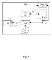
- FIG. 3 illustrates selected details of an embodiment of a system providing encryption key destruction for secure data erasure via physical removal of key information, with the system operating in a storage device mode. Elements of FIG. 3 are similar to FIG. 1C , except Key Storage KS 2 is implemented via Smartcard 302 electrically and mechanically coupled to Smartcard Interface 303 . In some embodiments, a seal is optionally used to detect removal of the removable component.
- the non-volatile memory, compatible socket, and interface may be a removable memory card (including, but not limited to MMC, SD, miniSD, microSD, and variants), other serial flash or EEPROM memory (including but not limited to SPI or I2C interfaces), and other non-volatile types.
- FIG. 4 illustrates the system of FIG. 3 , with the system operating with key information physically removed.
- the Smartcard has been removed, thus disabling access to any data encrypted using key material on KS 2 , as the encrypted data is no longer accessible without the key material.
- the Smartcard is destroyed, such as by mechanical or electrical techniques, to permanently prevent decryption of the encrypted data, thus providing secure erase of any data encrypted with the destroyed key material.
- FIG. 5 illustrates selected details of an embodiment of powering up and booting firmware implementing cryptographic functions.
- the cryptographic functions enable, for example, encryption/decryption of data according to key information stored in Key Storage KS 1 and Key Storage KS 2 , as performed by systems as illustrated in FIG. 1C and/or FIG. 3 .
- various combinations of all or portions of operations performed by a secure erasing device (such as Eraser Device 202 of FIG. 2 ), and portions of a processor, microprocessor, system-on-a-chip, application-specific-integrated-circuit, hardware accelerator, or other circuitry providing all or portions of the aforementioned operations, are specified by a specification compatible with processing by a computer system.
- the specification is in accordance with various descriptions, such as hardware description languages, circuit descriptions, netlist descriptions, mask descriptions, or layout descriptions.
- Example descriptions include: Verilog, VHDL, SPICE, SPICE variants such as PSpice, IBIS, LEF, DEF, GDS-II, OASIS, or other descriptions.
- the processing includes any combination of interpretation, compilation, simulation, and synthesis to produce, to verify, or to specify logic and/or circuitry suitable for inclusion on one or more integrated circuits.
- Each integrated circuit is designable and/or manufacturable according to a variety of techniques.
- the techniques include a programmable technique (such as a field or mask programmable gate array integrated circuit), a semi-custom technique (such as a wholly or partially cell-based integrated circuit), and a full-custom technique (such as an integrated circuit that is substantially specialized), any combination thereof, or any other technique compatible with design and/or manufacturing of integrated circuits.
- various combinations of all or portions of operations as described by a computer readable medium having a set of instructions stored therein are performed by execution and/or interpretation of one or more program instructions, by interpretation and/or compiling of one or more source and/or script language statements, or by execution of binary instructions produced by compiling, translating, and/or interpreting information expressed in programming and/or scripting language statements.
- the statements are compatible with any standard programming or scripting language (such as C, C++, Fortran, Pascal, Ada, Java, VBscript, and Shell).
- One or more of the program instructions, the language statements, or the binary instructions are optionally stored on one or more computer readable storage medium elements.
- some, all, or various portions of the program instructions are realized as one or more functions, routines, sub-routines, in-line routines, procedures, macros, or portions thereof.
- interconnect and function-unit bit-widths, clock speeds, and the type of technology used are variable according to various embodiments in each component block.
- the names given to interconnect and logic are merely exemplary, and should not be construed as limiting the concepts described.
- the order and arrangement of flowchart and flow diagram process, action, and function elements are variable according to various embodiments.
- value ranges specified, maximum and minimum values used, or other particular specifications are merely those of the described embodiments, are expected to track improvements and changes in implementation technology, and should not be construed as limitations.
Landscapes
- Engineering & Computer Science (AREA)
- Theoretical Computer Science (AREA)
- Computer Security & Cryptography (AREA)
- Computer Hardware Design (AREA)
- General Physics & Mathematics (AREA)
- General Engineering & Computer Science (AREA)
- Physics & Mathematics (AREA)
- Software Systems (AREA)
- Health & Medical Sciences (AREA)
- Bioethics (AREA)
- General Health & Medical Sciences (AREA)
- Computer Networks & Wireless Communication (AREA)
- Signal Processing (AREA)
- Storage Device Security (AREA)
Abstract
Description
-
- U.S. Provisional Application Ser. No. 61/383,017, filed 15 Sep. 2010, first named inventor Dmitry OBUKHOV, and entitled ENCRYPTION KEY DESTRUCTION FOR SECURE DATA ERASURE.
| Acronym | Description |
| EEPROM | Electrically Erasable Programmable Read Only randomly |
| accessible Memory | |
| FIPS | Federal Information Processing Standards |
| HDD | Hard Disk Drive |
| NVRAM | Non-Volatile Read/write randomly Accessible Memory |
| PCB | Printed Circuit Board |
| SATA | Serial Advanced Technology Attachment (Serial ATA) |
| SSD | Solid State Disk |
| TPM | Trusted Platform Module |
-
- a storage device enabled to encrypt and decrypt data according to a cryptographic key stored at least in part in an included non-volatile memory, the storage device having an external interface;
- an eraser device, separate from the storage device, and enabled to couple to the external interface; and
- wherein the eraser device is further enabled to destroy at least the part of the cryptographic key stored in the non-volatile memory, the destroying via at least partial erasure of the non-volatile memory.
-
- a removable component comprising a non-volatile memory enabled to store at least a portion of a cryptographic key;
- a storage device enabled to encrypt and decrypt data according to the cryptographic key, the storage device having an interface compatible with the removable component;
- a seal mechanism to detect uncoupling of the removable component from the interface; and
- wherein the cryptographic key is destroyable by mechanical manipulation or electrical overstressing of the removable component.
-
- encrypting data for storage in a storage device, the encrypting being in accordance with key material, the encrypting being within a secure facility;
- detecting one or more failures of the storage device;
- destroying, in response to the detecting, the key material; and
- transporting, after the destroying, the storage device outside of the secure facility.
-
- operating a storage device to store encrypted data;
- determining that at least a portion of the storage device is inoperable;
- destroying, after the determining, key material used to decrypt the encrypted data; and
- repairing, after the destroying, the storage device after the destroying.
-
- requiring first-user authentication and two key stores held in respective storage media to initialize a storage drive;
- operating the storage drive normally to encrypt and decrypt first-user data using a cipher key generated as a function of the two key stores;
- determining that at least a portion of the storage device is inoperable;
- zeroizing one of the key stores via a key-store external interface, after the determining and without normal power; and wherein the first-user data is unrecoverable, including with the first user authentication.
-
- requiring first-user authentication and two key stores held in respective storage media to initialize a storage drive;
- operating the storage drive normally to encrypt and decrypt first-user data using a cipher key generated as a function of the two key stores;
- determining that at least a portion of the storage device is inoperable;
- zeroizing one of the key stores via a key-store external interface, after the determining and without normal power, such that the first-user data is unrecoverable, including with the first user authentication; and
- restoring the drive to normal operation with respect to second-user data requiring second-user authentication.
System
Claims (27)
Priority Applications (2)
| Application Number | Priority Date | Filing Date | Title |
|---|---|---|---|
| US13/234,134 US8938624B2 (en) | 2010-09-15 | 2011-09-15 | Encryption key destruction for secure data erasure |
| US14/599,499 US9467288B2 (en) | 2010-09-15 | 2015-01-17 | Encryption key destruction for secure data erasure |
Applications Claiming Priority (2)
| Application Number | Priority Date | Filing Date | Title |
|---|---|---|---|
| US38301710P | 2010-09-15 | 2010-09-15 | |
| US13/234,134 US8938624B2 (en) | 2010-09-15 | 2011-09-15 | Encryption key destruction for secure data erasure |
Related Child Applications (1)
| Application Number | Title | Priority Date | Filing Date |
|---|---|---|---|
| US14/599,499 Continuation US9467288B2 (en) | 2010-09-15 | 2015-01-17 | Encryption key destruction for secure data erasure |
Publications (2)
| Publication Number | Publication Date |
|---|---|
| US20120093318A1 US20120093318A1 (en) | 2012-04-19 |
| US8938624B2 true US8938624B2 (en) | 2015-01-20 |
Family
ID=45934164
Family Applications (2)
| Application Number | Title | Priority Date | Filing Date |
|---|---|---|---|
| US13/234,134 Active 2031-11-27 US8938624B2 (en) | 2010-09-15 | 2011-09-15 | Encryption key destruction for secure data erasure |
| US14/599,499 Active US9467288B2 (en) | 2010-09-15 | 2015-01-17 | Encryption key destruction for secure data erasure |
Family Applications After (1)
| Application Number | Title | Priority Date | Filing Date |
|---|---|---|---|
| US14/599,499 Active US9467288B2 (en) | 2010-09-15 | 2015-01-17 | Encryption key destruction for secure data erasure |
Country Status (1)
| Country | Link |
|---|---|
| US (2) | US8938624B2 (en) |
Cited By (11)
| Publication number | Priority date | Publication date | Assignee | Title |
|---|---|---|---|---|
| US20150304108A1 (en) * | 2010-09-15 | 2015-10-22 | Seagate Technology Llc | Encryption Key Destruction For Secure Data Erasure |
| US20160378692A1 (en) * | 2013-12-08 | 2016-12-29 | Intel Corporation | Instructions and Logic to Provide Memory Access Key Protection Functionality |
| CN107590398A (en) * | 2017-09-26 | 2018-01-16 | 北京旅之星业新技术有限公司 | A kind of off line had both ruined the encryption safe storage method and device of key |
| US10133681B2 (en) | 2016-07-22 | 2018-11-20 | Seagate Technology Llc | Using encryption keys to manage data retention |
| US10373528B2 (en) | 2016-12-14 | 2019-08-06 | Western Digital Technologies, Inc. | Cell-level realization of burn after reading for NAND flash |
| US10536538B2 (en) | 2016-09-16 | 2020-01-14 | Microsoft Technology Licensing, Llc | Secure data erasure verification in hyperscale computing systems |
| US20220222384A1 (en) * | 2021-01-11 | 2022-07-14 | Micron Technology, Inc. | Encrypted key management |
| US12014059B2 (en) | 2021-12-20 | 2024-06-18 | Samsung Electronics Co., Ltd. | Storage devices, methods of operating storage devices, and methods of operating host devices |
| US12073095B2 (en) * | 2021-11-16 | 2024-08-27 | Samsung Electronics Co., Ltd. | Storage device performing a data protection operation and operation method thereof |
| US12321616B2 (en) | 2020-12-01 | 2025-06-03 | Micron Technology, Inc. | Memory systems and devices including examples of accessing memory and generating access codes using an authenticated stream cipher |
| US12541470B2 (en) | 2023-09-12 | 2026-02-03 | Samsung Electronics Co., Ltd. | Security-enhanced storage device |
Families Citing this family (116)
| Publication number | Priority date | Publication date | Assignee | Title |
|---|---|---|---|---|
| US20120069995A1 (en) * | 2010-09-22 | 2012-03-22 | Seagate Technology Llc | Controller chip with zeroizable root key |
| US20120079289A1 (en) * | 2010-09-27 | 2012-03-29 | Skymedi Corporation | Secure erase system for a solid state non-volatile memory device |
| DE102010048784B4 (en) * | 2010-10-18 | 2012-06-28 | Fraunhofer-Gesellschaft zur Förderung der angewandten Forschung e.V. | Sample carrier with sample data encryption and method for its use |
| US8909942B1 (en) * | 2012-03-30 | 2014-12-09 | Western Digital Technologies, Inc. | MRAM-based security for data storage systems |
| US8918651B2 (en) * | 2012-05-14 | 2014-12-23 | International Business Machines Corporation | Cryptographic erasure of selected encrypted data |
| US20140052899A1 (en) * | 2012-08-18 | 2014-02-20 | Yen Chih Nan | Memory address translation method for flash storage system |
| US20140064489A1 (en) * | 2012-08-31 | 2014-03-06 | High Density Devices As | Method, system and device for encryption key material erasure |
| US20140068277A1 (en) * | 2012-09-04 | 2014-03-06 | Markus T. Metzger | Secure Deletion of Data Stored in a Memory |
| US9798294B2 (en) * | 2012-09-18 | 2017-10-24 | Nxp B.V. | System, method and computer program product for detecting tampering in a product |
| TWM466297U (en) * | 2013-03-29 | 2013-11-21 | Sk Hynix Inc | Storage device with independent information storage space |
| US9990382B1 (en) * | 2013-04-10 | 2018-06-05 | Amazon Technologies, Inc. | Secure erasure and repair of non-mechanical storage media |
| US20140365743A1 (en) * | 2013-06-11 | 2014-12-11 | Seagate Technology Llc | Secure Erasure of Processing Devices |
| US9164694B1 (en) | 2013-06-19 | 2015-10-20 | Western Digital Technologies, Inc. | Data storage device detecting read-before-write conditions and returning configurable return data |
| US9323958B2 (en) * | 2013-07-22 | 2016-04-26 | Enterprise Sciences, Inc. | Method and apparatus for prevention of tampering and unauthorized use, and unauthorized extraction of information from secured devices |
| US20150089245A1 (en) * | 2013-09-26 | 2015-03-26 | Asher M. Altman | Data storage in persistent memory |
| GB2520489A (en) | 2013-11-20 | 2015-05-27 | Ibm | Deletion of content in digital storage systems |
| US10110382B1 (en) | 2014-09-02 | 2018-10-23 | Amazon Technologies, Inc. | Durable cryptographic keys |
| US10003584B1 (en) * | 2014-09-02 | 2018-06-19 | Amazon Technologies, Inc. | Durable key management |
| US10438106B2 (en) | 2014-11-04 | 2019-10-08 | Intellignet Technologies International, Inc. | Smartcard |
| US9762548B2 (en) * | 2015-03-13 | 2017-09-12 | Western Digital Technologies, Inc. | Controlling encrypted data stored on a remote storage device |
| CN106155812A (en) | 2015-04-28 | 2016-11-23 | 阿里巴巴集团控股有限公司 | Method, device, system and the electronic equipment of a kind of resource management to fictitious host computer |
| US10089481B2 (en) | 2015-09-23 | 2018-10-02 | International Business Machines Corporation | Securing recorded data |
| US10535713B2 (en) | 2015-09-30 | 2020-01-14 | International Business Machines Corporation | Integrated reactive material erasure element with phase change memory |
| JP2017078958A (en) | 2015-10-20 | 2017-04-27 | 株式会社東芝 | Semiconductor device |
| US9892276B2 (en) | 2015-11-11 | 2018-02-13 | International Business Machines Corporation | Verifiable data destruction in a database |
| JP6568461B2 (en) * | 2015-11-18 | 2019-08-28 | 株式会社アイ・オー・データ機器 | Nonvolatile semiconductor memory storage device |
| US9941004B2 (en) | 2015-12-30 | 2018-04-10 | International Business Machines Corporation | Integrated arming switch and arming switch activation layer for secure memory |
| US9971899B2 (en) | 2016-01-04 | 2018-05-15 | International Business Machines Corporation | Secure, targeted, customizable data removal |
| US10142304B2 (en) | 2016-08-23 | 2018-11-27 | Seagate Technology Llc | Encryption key shredding to protect non-persistent data |
| US9720700B1 (en) * | 2016-10-05 | 2017-08-01 | Apricorn | Secure storage devices, with physical input device, for secure configuration in a configuration-ready mode |
| US10607018B2 (en) * | 2016-10-11 | 2020-03-31 | Xitore, Inc. | Apparatus, system, and method of securitization of memory modules against malicious acts |
| CN106529332B (en) * | 2016-10-25 | 2019-08-13 | Oppo广东移动通信有限公司 | A kind of authority control method of mobile terminal, device and mobile terminal |
| US10474831B1 (en) * | 2016-11-28 | 2019-11-12 | Amazon Technologies, Inc. | Large network attached storage encryption |
| US10706153B2 (en) * | 2017-05-25 | 2020-07-07 | Dell Products L.P. | Preventing malicious cryptographic erasure of storage devices |
| US10185509B1 (en) * | 2017-06-01 | 2019-01-22 | Amazon Technologies, Inc. | Secure storage device sanitization |
| US10587590B2 (en) * | 2017-06-12 | 2020-03-10 | Seagate Technology Llc | Tracking of data erasures |
| US10884926B2 (en) | 2017-06-16 | 2021-01-05 | Alibaba Group Holding Limited | Method and system for distributed storage using client-side global persistent cache |
| US10678443B2 (en) | 2017-07-06 | 2020-06-09 | Alibaba Group Holding Limited | Method and system for high-density converged storage via memory bus |
| US10248553B2 (en) * | 2017-07-14 | 2019-04-02 | International Business Machines Corporation | Test methodology for detection of unwanted cryptographic key destruction |
| US10216967B2 (en) * | 2017-07-25 | 2019-02-26 | The United States Of America As Represented By The Secretary Of The Navy | Volatile memory-based data-transfer device with automatic and user-initiated anti-tamper penalties |
| US10496829B2 (en) * | 2017-09-15 | 2019-12-03 | Alibaba Group Holding Limited | Method and system for data destruction in a phase change memory-based storage device |
| US10642522B2 (en) | 2017-09-15 | 2020-05-05 | Alibaba Group Holding Limited | Method and system for in-line deduplication in a storage drive based on a non-collision hash |
| US10789011B2 (en) | 2017-09-27 | 2020-09-29 | Alibaba Group Holding Limited | Performance enhancement of a storage device using an integrated controller-buffer |
| US10860334B2 (en) | 2017-10-25 | 2020-12-08 | Alibaba Group Holding Limited | System and method for centralized boot storage in an access switch shared by multiple servers |
| US10877898B2 (en) | 2017-11-16 | 2020-12-29 | Alibaba Group Holding Limited | Method and system for enhancing flash translation layer mapping flexibility for performance and lifespan improvements |
| CN109831300A (en) * | 2017-11-23 | 2019-05-31 | 航天信息股份有限公司 | A kind of cipher key destruction method and device |
| US11017127B2 (en) * | 2018-01-31 | 2021-05-25 | Seagate Technology Llc | Storage compute appliance with internal data encryption |
| US10891239B2 (en) | 2018-02-07 | 2021-01-12 | Alibaba Group Holding Limited | Method and system for operating NAND flash physical space to extend memory capacity |
| US10496548B2 (en) | 2018-02-07 | 2019-12-03 | Alibaba Group Holding Limited | Method and system for user-space storage I/O stack with user-space flash translation layer |
| US10831404B2 (en) | 2018-02-08 | 2020-11-10 | Alibaba Group Holding Limited | Method and system for facilitating high-capacity shared memory using DIMM from retired servers |
| US11049565B2 (en) | 2018-04-23 | 2021-06-29 | Micron Technology, Inc. | Non-volatile memory devices and systems with volatile memory features and methods for operating the same |
| US10446248B1 (en) | 2018-04-23 | 2019-10-15 | Micron Technology, Inc. | Non-volatile memory devices and systems with read-only memory features and methods for operating the same |
| WO2019222958A1 (en) | 2018-05-24 | 2019-11-28 | Alibaba Group Holding Limited | System and method for flash storage management using multiple open page stripes |
| US11816043B2 (en) | 2018-06-25 | 2023-11-14 | Alibaba Group Holding Limited | System and method for managing resources of a storage device and quantifying the cost of I/O requests |
| US10921992B2 (en) | 2018-06-25 | 2021-02-16 | Alibaba Group Holding Limited | Method and system for data placement in a hard disk drive based on access frequency for improved IOPS and utilization efficiency |
| US10871921B2 (en) | 2018-07-30 | 2020-12-22 | Alibaba Group Holding Limited | Method and system for facilitating atomicity assurance on metadata and data bundled storage |
| US10747673B2 (en) | 2018-08-02 | 2020-08-18 | Alibaba Group Holding Limited | System and method for facilitating cluster-level cache and memory space |
| US10996886B2 (en) | 2018-08-02 | 2021-05-04 | Alibaba Group Holding Limited | Method and system for facilitating atomicity and latency assurance on variable sized I/O |
| US11327929B2 (en) | 2018-09-17 | 2022-05-10 | Alibaba Group Holding Limited | Method and system for reduced data movement compression using in-storage computing and a customized file system |
| US10852948B2 (en) | 2018-10-19 | 2020-12-01 | Alibaba Group Holding | System and method for data organization in shingled magnetic recording drive |
| US10795586B2 (en) | 2018-11-19 | 2020-10-06 | Alibaba Group Holding Limited | System and method for optimization of global data placement to mitigate wear-out of write cache and NAND flash |
| US10769018B2 (en) | 2018-12-04 | 2020-09-08 | Alibaba Group Holding Limited | System and method for handling uncorrectable data errors in high-capacity storage |
| US10872175B2 (en) | 2018-12-06 | 2020-12-22 | Fortanix, Inc. | Erasing a cryptographic item in a memory of a device in response to a change of an operating mode of the device |
| US10977122B2 (en) | 2018-12-31 | 2021-04-13 | Alibaba Group Holding Limited | System and method for facilitating differentiated error correction in high-density flash devices |
| US10884654B2 (en) | 2018-12-31 | 2021-01-05 | Alibaba Group Holding Limited | System and method for quality of service assurance of multi-stream scenarios in a hard disk drive |
| US11061735B2 (en) | 2019-01-02 | 2021-07-13 | Alibaba Group Holding Limited | System and method for offloading computation to storage nodes in distributed system |
| US11132291B2 (en) | 2019-01-04 | 2021-09-28 | Alibaba Group Holding Limited | System and method of FPGA-executed flash translation layer in multiple solid state drives |
| US11455402B2 (en) | 2019-01-30 | 2022-09-27 | Seagate Technology Llc | Non-volatile memory with precise write-once protection |
| US10860420B2 (en) | 2019-02-05 | 2020-12-08 | Alibaba Group Holding Limited | Method and system for mitigating read disturb impact on persistent memory |
| US11200337B2 (en) | 2019-02-11 | 2021-12-14 | Alibaba Group Holding Limited | System and method for user data isolation |
| US10970212B2 (en) | 2019-02-15 | 2021-04-06 | Alibaba Group Holding Limited | Method and system for facilitating a distributed storage system with a total cost of ownership reduction for multiple available zones |
| US11061834B2 (en) | 2019-02-26 | 2021-07-13 | Alibaba Group Holding Limited | Method and system for facilitating an improved storage system by decoupling the controller from the storage medium |
| US10783035B1 (en) | 2019-02-28 | 2020-09-22 | Alibaba Group Holding Limited | Method and system for improving throughput and reliability of storage media with high raw-error-rate |
| US10891065B2 (en) | 2019-04-01 | 2021-01-12 | Alibaba Group Holding Limited | Method and system for online conversion of bad blocks for improvement of performance and longevity in a solid state drive |
| US10922234B2 (en) | 2019-04-11 | 2021-02-16 | Alibaba Group Holding Limited | Method and system for online recovery of logical-to-physical mapping table affected by noise sources in a solid state drive |
| US10908960B2 (en) | 2019-04-16 | 2021-02-02 | Alibaba Group Holding Limited | Resource allocation based on comprehensive I/O monitoring in a distributed storage system |
| US11169873B2 (en) | 2019-05-21 | 2021-11-09 | Alibaba Group Holding Limited | Method and system for extending lifespan and enhancing throughput in a high-density solid state drive |
| US10860223B1 (en) | 2019-07-18 | 2020-12-08 | Alibaba Group Holding Limited | Method and system for enhancing a distributed storage system by decoupling computation and network tasks |
| US11074124B2 (en) | 2019-07-23 | 2021-07-27 | Alibaba Group Holding Limited | Method and system for enhancing throughput of big data analysis in a NAND-based read source storage |
| US12047492B2 (en) | 2019-09-13 | 2024-07-23 | International Business Machines Corporation | Crypto-erasure via internal and/or external action |
| US10608819B1 (en) | 2019-09-24 | 2020-03-31 | Apricorn | Portable storage device with internal secure controller that performs self-verification and self-generates encryption key(s) without using host or memory controller and that securely sends encryption key(s) via side channel |
| US11126561B2 (en) | 2019-10-01 | 2021-09-21 | Alibaba Group Holding Limited | Method and system for organizing NAND blocks and placing data to facilitate high-throughput for random writes in a solid state drive |
| US10656854B1 (en) | 2019-10-22 | 2020-05-19 | Apricorn | Method and portable storage device with internal controller that can self-verify the device and self-convert the device from current mode to renewed mode without communicating with host |
| JP6954340B2 (en) * | 2019-11-07 | 2021-10-27 | 日本電気株式会社 | Memory device management system, memory device management methods and programs |
| US11042307B1 (en) | 2020-01-13 | 2021-06-22 | Alibaba Group Holding Limited | System and method for facilitating improved utilization of NAND flash based on page-wise operation |
| US11449455B2 (en) | 2020-01-15 | 2022-09-20 | Alibaba Group Holding Limited | Method and system for facilitating a high-capacity object storage system with configuration agility and mixed deployment flexibility |
| US10872622B1 (en) | 2020-02-19 | 2020-12-22 | Alibaba Group Holding Limited | Method and system for deploying mixed storage products on a uniform storage infrastructure |
| US10923156B1 (en) | 2020-02-19 | 2021-02-16 | Alibaba Group Holding Limited | Method and system for facilitating low-cost high-throughput storage for accessing large-size I/O blocks in a hard disk drive |
| US11150986B2 (en) | 2020-02-26 | 2021-10-19 | Alibaba Group Holding Limited | Efficient compaction on log-structured distributed file system using erasure coding for resource consumption reduction |
| US11144250B2 (en) | 2020-03-13 | 2021-10-12 | Alibaba Group Holding Limited | Method and system for facilitating a persistent memory-centric system |
| US11200114B2 (en) | 2020-03-17 | 2021-12-14 | Alibaba Group Holding Limited | System and method for facilitating elastic error correction code in memory |
| JP2021149417A (en) * | 2020-03-18 | 2021-09-27 | キオクシア株式会社 | Storage device and control method |
| KR102880722B1 (en) | 2020-03-30 | 2025-11-06 | 삼성전자주식회사 | Storage device, and data destruction method thereof |
| KR20210127278A (en) * | 2020-04-13 | 2021-10-22 | 삼성전자주식회사 | Storage device, and data disposal method thereof |
| US11385833B2 (en) | 2020-04-20 | 2022-07-12 | Alibaba Group Holding Limited | Method and system for facilitating a light-weight garbage collection with a reduced utilization of resources |
| KR102777277B1 (en) | 2020-04-28 | 2025-03-10 | 삼성전자주식회사 | Storage device providing safe discard of data and Operating method thereof |
| US11281575B2 (en) | 2020-05-11 | 2022-03-22 | Alibaba Group Holding Limited | Method and system for facilitating data placement and control of physical addresses with multi-queue I/O blocks |
| US11494115B2 (en) | 2020-05-13 | 2022-11-08 | Alibaba Group Holding Limited | System method for facilitating memory media as file storage device based on real-time hashing by performing integrity check with a cyclical redundancy check (CRC) |
| US11461262B2 (en) | 2020-05-13 | 2022-10-04 | Alibaba Group Holding Limited | Method and system for facilitating a converged computation and storage node in a distributed storage system |
| US11218165B2 (en) | 2020-05-15 | 2022-01-04 | Alibaba Group Holding Limited | Memory-mapped two-dimensional error correction code for multi-bit error tolerance in DRAM |
| US11556277B2 (en) | 2020-05-19 | 2023-01-17 | Alibaba Group Holding Limited | System and method for facilitating improved performance in ordering key-value storage with input/output stack simplification |
| US11507499B2 (en) | 2020-05-19 | 2022-11-22 | Alibaba Group Holding Limited | System and method for facilitating mitigation of read/write amplification in data compression |
| US11263132B2 (en) | 2020-06-11 | 2022-03-01 | Alibaba Group Holding Limited | Method and system for facilitating log-structure data organization |
| US11354200B2 (en) | 2020-06-17 | 2022-06-07 | Alibaba Group Holding Limited | Method and system for facilitating data recovery and version rollback in a storage device |
| US11422931B2 (en) | 2020-06-17 | 2022-08-23 | Alibaba Group Holding Limited | Method and system for facilitating a physically isolated storage unit for multi-tenancy virtualization |
| US11354233B2 (en) | 2020-07-27 | 2022-06-07 | Alibaba Group Holding Limited | Method and system for facilitating fast crash recovery in a storage device |
| US11372774B2 (en) | 2020-08-24 | 2022-06-28 | Alibaba Group Holding Limited | Method and system for a solid state drive with on-chip memory integration |
| US11487465B2 (en) | 2020-12-11 | 2022-11-01 | Alibaba Group Holding Limited | Method and system for a local storage engine collaborating with a solid state drive controller |
| US11734115B2 (en) | 2020-12-28 | 2023-08-22 | Alibaba Group Holding Limited | Method and system for facilitating write latency reduction in a queue depth of one scenario |
| US11416365B2 (en) | 2020-12-30 | 2022-08-16 | Alibaba Group Holding Limited | Method and system for open NAND block detection and correction in an open-channel SSD |
| US11726699B2 (en) | 2021-03-30 | 2023-08-15 | Alibaba Singapore Holding Private Limited | Method and system for facilitating multi-stream sequential read performance improvement with reduced read amplification |
| US11461173B1 (en) | 2021-04-21 | 2022-10-04 | Alibaba Singapore Holding Private Limited | Method and system for facilitating efficient data compression based on error correction code and reorganization of data placement |
| US11476874B1 (en) | 2021-05-14 | 2022-10-18 | Alibaba Singapore Holding Private Limited | Method and system for facilitating a storage server with hybrid memory for journaling and data storage |
| US20220376908A1 (en) * | 2021-05-24 | 2022-11-24 | Softiron Limited | Secure Disk Erasure |
| IL291459A (en) * | 2022-03-17 | 2023-10-01 | Kazuar Advanced Tech Ltd | Key management system |
| CN116779003B (en) * | 2023-06-21 | 2023-12-08 | 广州市动易网络科技有限公司 | Method and system for hard disk data destruction and security assessment |
Citations (20)
| Publication number | Priority date | Publication date | Assignee | Title |
|---|---|---|---|---|
| US4301486A (en) * | 1979-06-04 | 1981-11-17 | Texas Instruments, Inc. | System for recording information on a flexible information storage media |
| US4593384A (en) * | 1984-12-21 | 1986-06-03 | Ncr Corporation | Security device for the secure storage of sensitive data |
| US4811288A (en) * | 1985-09-25 | 1989-03-07 | Ncr Corporation | Data security device for protecting stored data |
| US5469557A (en) * | 1993-03-05 | 1995-11-21 | Microchip Technology Incorporated | Code protection in microcontroller with EEPROM fuses |
| US6234389B1 (en) * | 1998-04-29 | 2001-05-22 | @Pos.Com, Inc. | PCMCIA-based point of sale transaction system |
| US6757832B1 (en) * | 2000-02-15 | 2004-06-29 | Silverbrook Research Pty Ltd | Unauthorized modification of values in flash memory |
| US20050195975A1 (en) * | 2003-01-21 | 2005-09-08 | Kevin Kawakita | Digital media distribution cryptography using media ticket smart cards |
| US7246098B1 (en) * | 1997-07-15 | 2007-07-17 | Silverbrook Research Pty Ltd | Consumable authentication protocol and system |
| US20080129037A1 (en) * | 2006-12-01 | 2008-06-05 | Prime Technology Llc | Tagging items with a security feature |
| US7494062B2 (en) * | 2006-11-17 | 2009-02-24 | Ncr Corporation | Secure reader for use in data management |
| US20090057421A1 (en) * | 2007-09-04 | 2009-03-05 | Suorsa Peter A | Data management |
| US20090106563A1 (en) * | 2007-10-17 | 2009-04-23 | Spansion Llc | Tamper reactive memory device to secure data from tamper attacks |
| US20090327756A1 (en) * | 2008-05-16 | 2009-12-31 | Stuart Pekowsky | Secure digital content storage device |
| US7743262B2 (en) * | 1997-07-15 | 2010-06-22 | Silverbrook Research Pty Ltd | Integrated circuit incorporating protection from power supply attacks |
| US7747541B2 (en) * | 1997-07-15 | 2010-06-29 | Silverbrook Research Pty Ltd | Validating apparatus for use with a pair of integrated circuits |
| US7757084B2 (en) * | 2000-02-15 | 2010-07-13 | Silverbrook Research Pty Ltd | Method of validating consumable authentication chip |
| US7805609B2 (en) * | 2006-11-17 | 2010-09-28 | Ncr Corporation | Data management |
| US7845553B2 (en) * | 2006-11-17 | 2010-12-07 | Ncr Corporation | Data management |
| US7962767B2 (en) * | 1997-07-15 | 2011-06-14 | Silverbrook Research Pty Ltd | Integrated circuit having obscured state change circuitry |
| US8127151B2 (en) * | 2009-10-13 | 2012-02-28 | Lockheed Martin Corporation | Hardware-based key generation and recovery |
Family Cites Families (7)
| Publication number | Priority date | Publication date | Assignee | Title |
|---|---|---|---|---|
| US8539250B2 (en) * | 2007-09-29 | 2013-09-17 | Intel Corporation | Secure, two-stage storage system |
| US8938624B2 (en) * | 2010-09-15 | 2015-01-20 | Lsi Corporation | Encryption key destruction for secure data erasure |
| US9160524B2 (en) * | 2011-05-02 | 2015-10-13 | George Mason University | Method and system for recovering cryptographic operations and/or secrets |
| JP5900509B2 (en) * | 2011-12-06 | 2016-04-06 | 富士通株式会社 | Node, communication method, and communication system |
| US20150006911A1 (en) * | 2013-06-28 | 2015-01-01 | Lexmark International, Inc. | Wear Leveling Non-Volatile Memory and Secure Erase of Data |
| US8964237B2 (en) * | 2013-06-28 | 2015-02-24 | Lexmark International, Inc. | Imaging device including wear leveling for non-volatile memory and secure erase of data |
| US9363085B2 (en) * | 2013-11-25 | 2016-06-07 | Seagate Technology Llc | Attestation of data sanitization |
-
2011
- 2011-09-15 US US13/234,134 patent/US8938624B2/en active Active
-
2015
- 2015-01-17 US US14/599,499 patent/US9467288B2/en active Active
Patent Citations (23)
| Publication number | Priority date | Publication date | Assignee | Title |
|---|---|---|---|---|
| US4301486A (en) * | 1979-06-04 | 1981-11-17 | Texas Instruments, Inc. | System for recording information on a flexible information storage media |
| US4593384A (en) * | 1984-12-21 | 1986-06-03 | Ncr Corporation | Security device for the secure storage of sensitive data |
| US4811288A (en) * | 1985-09-25 | 1989-03-07 | Ncr Corporation | Data security device for protecting stored data |
| US5469557A (en) * | 1993-03-05 | 1995-11-21 | Microchip Technology Incorporated | Code protection in microcontroller with EEPROM fuses |
| US7743262B2 (en) * | 1997-07-15 | 2010-06-22 | Silverbrook Research Pty Ltd | Integrated circuit incorporating protection from power supply attacks |
| US7962767B2 (en) * | 1997-07-15 | 2011-06-14 | Silverbrook Research Pty Ltd | Integrated circuit having obscured state change circuitry |
| US7747541B2 (en) * | 1997-07-15 | 2010-06-29 | Silverbrook Research Pty Ltd | Validating apparatus for use with a pair of integrated circuits |
| US7246098B1 (en) * | 1997-07-15 | 2007-07-17 | Silverbrook Research Pty Ltd | Consumable authentication protocol and system |
| US6234389B1 (en) * | 1998-04-29 | 2001-05-22 | @Pos.Com, Inc. | PCMCIA-based point of sale transaction system |
| US6757832B1 (en) * | 2000-02-15 | 2004-06-29 | Silverbrook Research Pty Ltd | Unauthorized modification of values in flash memory |
| US7941661B2 (en) * | 2000-02-15 | 2011-05-10 | Silverbrook Research Pty Ltd | Method of testing validity of authentication IC |
| US7757084B2 (en) * | 2000-02-15 | 2010-07-13 | Silverbrook Research Pty Ltd | Method of validating consumable authentication chip |
| US7093139B2 (en) * | 2000-02-15 | 2006-08-15 | Silverbrook Research Pty Ltd | Unauthorized modification of values stored in flash memory |
| US20050195975A1 (en) * | 2003-01-21 | 2005-09-08 | Kevin Kawakita | Digital media distribution cryptography using media ticket smart cards |
| US7805609B2 (en) * | 2006-11-17 | 2010-09-28 | Ncr Corporation | Data management |
| US7845553B2 (en) * | 2006-11-17 | 2010-12-07 | Ncr Corporation | Data management |
| US7494062B2 (en) * | 2006-11-17 | 2009-02-24 | Ncr Corporation | Secure reader for use in data management |
| US20080129037A1 (en) * | 2006-12-01 | 2008-06-05 | Prime Technology Llc | Tagging items with a security feature |
| US20090057421A1 (en) * | 2007-09-04 | 2009-03-05 | Suorsa Peter A | Data management |
| US20090106563A1 (en) * | 2007-10-17 | 2009-04-23 | Spansion Llc | Tamper reactive memory device to secure data from tamper attacks |
| US7945792B2 (en) * | 2007-10-17 | 2011-05-17 | Spansion Llc | Tamper reactive memory device to secure data from tamper attacks |
| US20090327756A1 (en) * | 2008-05-16 | 2009-12-31 | Stuart Pekowsky | Secure digital content storage device |
| US8127151B2 (en) * | 2009-10-13 | 2012-02-28 | Lockheed Martin Corporation | Hardware-based key generation and recovery |
Cited By (13)
| Publication number | Priority date | Publication date | Assignee | Title |
|---|---|---|---|---|
| US9467288B2 (en) * | 2010-09-15 | 2016-10-11 | Seagate Technology Llc | Encryption key destruction for secure data erasure |
| US20150304108A1 (en) * | 2010-09-15 | 2015-10-22 | Seagate Technology Llc | Encryption Key Destruction For Secure Data Erasure |
| US20160378692A1 (en) * | 2013-12-08 | 2016-12-29 | Intel Corporation | Instructions and Logic to Provide Memory Access Key Protection Functionality |
| US10756895B2 (en) | 2016-07-22 | 2020-08-25 | Seagate Technology Llc | Using encryption keys to manage data retention |
| US10133681B2 (en) | 2016-07-22 | 2018-11-20 | Seagate Technology Llc | Using encryption keys to manage data retention |
| US10536538B2 (en) | 2016-09-16 | 2020-01-14 | Microsoft Technology Licensing, Llc | Secure data erasure verification in hyperscale computing systems |
| US10373528B2 (en) | 2016-12-14 | 2019-08-06 | Western Digital Technologies, Inc. | Cell-level realization of burn after reading for NAND flash |
| CN107590398A (en) * | 2017-09-26 | 2018-01-16 | 北京旅之星业新技术有限公司 | A kind of off line had both ruined the encryption safe storage method and device of key |
| US12321616B2 (en) | 2020-12-01 | 2025-06-03 | Micron Technology, Inc. | Memory systems and devices including examples of accessing memory and generating access codes using an authenticated stream cipher |
| US20220222384A1 (en) * | 2021-01-11 | 2022-07-14 | Micron Technology, Inc. | Encrypted key management |
| US12073095B2 (en) * | 2021-11-16 | 2024-08-27 | Samsung Electronics Co., Ltd. | Storage device performing a data protection operation and operation method thereof |
| US12014059B2 (en) | 2021-12-20 | 2024-06-18 | Samsung Electronics Co., Ltd. | Storage devices, methods of operating storage devices, and methods of operating host devices |
| US12541470B2 (en) | 2023-09-12 | 2026-02-03 | Samsung Electronics Co., Ltd. | Security-enhanced storage device |
Also Published As
| Publication number | Publication date |
|---|---|
| US20150304108A1 (en) | 2015-10-22 |
| US20120093318A1 (en) | 2012-04-19 |
| US9467288B2 (en) | 2016-10-11 |
Similar Documents
| Publication | Publication Date | Title |
|---|---|---|
| US8938624B2 (en) | Encryption key destruction for secure data erasure | |
| US9069703B2 (en) | Encrypted-transport solid-state disk controller | |
| TWI584125B (en) | I/o device and computing host interoperation | |
| CN105159699B (en) | Management of device firmware update effects as seen by a host | |
| US9753869B2 (en) | Techniques for secure storage hijacking protection | |
| KR102155191B1 (en) | Management of and region selection for writes to non-volatile memory | |
| TWI479359B (en) | Command executing method, memory controller and memory storage apparatus | |
| US9430680B2 (en) | Tamper sensor | |
| US8954705B2 (en) | Memory space management method and memory controller and memory storage device and memory storage using the same | |
| TWI489272B (en) | Data protecting method, and memory controller and memory storage device using the same | |
| CN104346103A (en) | Instruction execution method, memory controller and memory storage device | |
| TWI486766B (en) | Data processing method, and memory controller and memory storage apparatus using the same | |
| US20130080787A1 (en) | Memory storage apparatus, memory controller and password verification method | |
| TWI521345B (en) | Method for reading response and data transmission system | |
| CN106033321A (en) | Response reading method and data transmission system | |
| CN103377149A (en) | method for protecting data, memory controller and memory storage device | |
| Firmware et al. | A Beginner’s Guide to SSD Firmware |
Legal Events
| Date | Code | Title | Description |
|---|---|---|---|
| AS | Assignment |
Owner name: SANDFORCE, INC., CALIFORNIA Free format text: ASSIGNMENT OF ASSIGNORS INTEREST;ASSIGNORS:OBUKHOV, DMITRY;TAN, BIN;REEL/FRAME:027400/0481 Effective date: 20111024 |
|
| AS | Assignment |
Owner name: LSI CORPORATION, CALIFORNIA Free format text: ASSIGNMENT OF ASSIGNORS INTEREST;ASSIGNOR:SANDFORCE, INC.;REEL/FRAME:029689/0926 Effective date: 20120104 |
|
| AS | Assignment |
Owner name: DEUTSCHE BANK AG NEW YORK BRANCH, AS COLLATERAL AGENT, NEW YORK Free format text: PATENT SECURITY AGREEMENT;ASSIGNORS:LSI CORPORATION;AGERE SYSTEMS LLC;REEL/FRAME:032856/0031 Effective date: 20140506 Owner name: DEUTSCHE BANK AG NEW YORK BRANCH, AS COLLATERAL AG Free format text: PATENT SECURITY AGREEMENT;ASSIGNORS:LSI CORPORATION;AGERE SYSTEMS LLC;REEL/FRAME:032856/0031 Effective date: 20140506 |
|
| AS | Assignment |
Owner name: AGERE SYSTEMS LLC, PENNSYLVANIA Free format text: TERMINATION AND RELEASE OF SECURITY INTEREST IN CERTAIN PATENTS INCLUDED IN SECURITY INTEREST PREVIOUSLY RECORDED AT REEL/FRAME (032856/0031);ASSIGNOR:DEUTSCHE BANK AG NEW YORK BRANCH, AS COLLATERAL AGENT;REEL/FRAME:034177/0257 Effective date: 20140902 Owner name: LSI CORPORATION, CALIFORNIA Free format text: TERMINATION AND RELEASE OF SECURITY INTEREST IN CERTAIN PATENTS INCLUDED IN SECURITY INTEREST PREVIOUSLY RECORDED AT REEL/FRAME (032856/0031);ASSIGNOR:DEUTSCHE BANK AG NEW YORK BRANCH, AS COLLATERAL AGENT;REEL/FRAME:034177/0257 Effective date: 20140902 |
|
| STCF | Information on status: patent grant |
Free format text: PATENTED CASE |
|
| AS | Assignment |
Owner name: SEAGATE TECHNOLOGY LLC, CALIFORNIA Free format text: ASSIGNMENT OF ASSIGNORS INTEREST;ASSIGNOR:LSI CORPORATION;REEL/FRAME:034771/0571 Effective date: 20140902 |
|
| AS | Assignment |
Owner name: LSI CORPORATION, CALIFORNIA Free format text: TERMINATION AND RELEASE OF SECURITY INTEREST IN PATENT RIGHTS (RELEASES RF 032856-0031);ASSIGNOR:DEUTSCHE BANK AG NEW YORK BRANCH, AS COLLATERAL AGENT;REEL/FRAME:037684/0039 Effective date: 20160201 Owner name: AGERE SYSTEMS LLC, PENNSYLVANIA Free format text: TERMINATION AND RELEASE OF SECURITY INTEREST IN PATENT RIGHTS (RELEASES RF 032856-0031);ASSIGNOR:DEUTSCHE BANK AG NEW YORK BRANCH, AS COLLATERAL AGENT;REEL/FRAME:037684/0039 Effective date: 20160201 |
|
| FEPP | Fee payment procedure |
Free format text: MAINTENANCE FEE REMINDER MAILED (ORIGINAL EVENT CODE: REM.); ENTITY STATUS OF PATENT OWNER: LARGE ENTITY |
|
| FEPP | Fee payment procedure |
Free format text: SURCHARGE FOR LATE PAYMENT, LARGE ENTITY (ORIGINAL EVENT CODE: M1554); ENTITY STATUS OF PATENT OWNER: LARGE ENTITY |
|
| MAFP | Maintenance fee payment |
Free format text: PAYMENT OF MAINTENANCE FEE, 4TH YEAR, LARGE ENTITY (ORIGINAL EVENT CODE: M1551); ENTITY STATUS OF PATENT OWNER: LARGE ENTITY Year of fee payment: 4 |
|
| MAFP | Maintenance fee payment |
Free format text: PAYMENT OF MAINTENANCE FEE, 8TH YEAR, LARGE ENTITY (ORIGINAL EVENT CODE: M1552); ENTITY STATUS OF PATENT OWNER: LARGE ENTITY Year of fee payment: 8 |