US8937511B2 - Frequency scaling of variable speed systems for fast response and power reduction - Google Patents
Frequency scaling of variable speed systems for fast response and power reduction Download PDFInfo
- Publication number
- US8937511B2 US8937511B2 US13/681,737 US201213681737A US8937511B2 US 8937511 B2 US8937511 B2 US 8937511B2 US 201213681737 A US201213681737 A US 201213681737A US 8937511 B2 US8937511 B2 US 8937511B2
- Authority
- US
- United States
- Prior art keywords
- amplifiers
- transconductance
- inverters
- processor
- frequency
- Prior art date
- Legal status (The legal status is an assumption and is not a legal conclusion. Google has not performed a legal analysis and makes no representation as to the accuracy of the status listed.)
- Expired - Fee Related, expires
Links
Images


Classifications
-
- H—ELECTRICITY
- H03—ELECTRONIC CIRCUITRY
- H03K—PULSE TECHNIQUE
- H03K3/00—Circuits for generating electric pulses; Monostable, bistable or multistable circuits
- H03K3/02—Generators characterised by the type of circuit or by the means used for producing pulses
-
- G—PHYSICS
- G06—COMPUTING OR CALCULATING; COUNTING
- G06F—ELECTRIC DIGITAL DATA PROCESSING
- G06F1/00—Details not covered by groups G06F3/00 - G06F13/00 and G06F21/00
- G06F1/04—Generating or distributing clock signals or signals derived directly therefrom
- G06F1/08—Clock generators with changeable or programmable clock frequency
-
- G—PHYSICS
- G06—COMPUTING OR CALCULATING; COUNTING
- G06F—ELECTRIC DIGITAL DATA PROCESSING
- G06F1/00—Details not covered by groups G06F3/00 - G06F13/00 and G06F21/00
- G06F1/26—Power supply means, e.g. regulation thereof
- G06F1/32—Means for saving power
- G06F1/3203—Power management, i.e. event-based initiation of a power-saving mode
- G06F1/3234—Power saving characterised by the action undertaken
- G06F1/324—Power saving characterised by the action undertaken by lowering clock frequency
-
- G—PHYSICS
- G06—COMPUTING OR CALCULATING; COUNTING
- G06F—ELECTRIC DIGITAL DATA PROCESSING
- G06F1/00—Details not covered by groups G06F3/00 - G06F13/00 and G06F21/00
- G06F1/26—Power supply means, e.g. regulation thereof
- G06F1/32—Means for saving power
- G06F1/3203—Power management, i.e. event-based initiation of a power-saving mode
- G06F1/3234—Power saving characterised by the action undertaken
- G06F1/3296—Power saving characterised by the action undertaken by lowering the supply or operating voltage
-
- Y—GENERAL TAGGING OF NEW TECHNOLOGICAL DEVELOPMENTS; GENERAL TAGGING OF CROSS-SECTIONAL TECHNOLOGIES SPANNING OVER SEVERAL SECTIONS OF THE IPC; TECHNICAL SUBJECTS COVERED BY FORMER USPC CROSS-REFERENCE ART COLLECTIONS [XRACs] AND DIGESTS
- Y02—TECHNOLOGIES OR APPLICATIONS FOR MITIGATION OR ADAPTATION AGAINST CLIMATE CHANGE
- Y02D—CLIMATE CHANGE MITIGATION TECHNOLOGIES IN INFORMATION AND COMMUNICATION TECHNOLOGIES [ICT], I.E. INFORMATION AND COMMUNICATION TECHNOLOGIES AIMING AT THE REDUCTION OF THEIR OWN ENERGY USE
- Y02D10/00—Energy efficient computing, e.g. low power processors, power management or thermal management
Definitions
- the present disclosure relates generally to power management in computing devices and more particularly to frequency scaling of variable speed systems for fast response and power reduction.
- Processors of computing devices including laptop computers, smartphones, and tablets can execute different applications.
- the power consumed by the computing devices depends on the speed of the processors.
- the speed of the processors can be varied depending on the applications being executed by the processors.
- a system comprises a plurality of amplifiers configured to generate a clock signal having a frequency.
- the clock signal is input to a processor.
- the amplifiers are connected in series. An output of a last one of the amplifiers is fed back to an input of a first one of the amplifiers.
- Each of the amplifiers has a transconductance.
- a frequency adjustment module is configured to adjust, based on an activity level of the processor, the frequency of the clock signal by adjusting the transconductance of the amplifiers.
- the plurality of amplifiers receives a supply voltage
- the system further comprises a supply voltage control module configured to adjust, based on the activity level of the processor, the transconductance of the amplifiers by adjusting the supply voltage of the plurality of amplifiers.
- each of the amplifiers includes an input configured to receive a control signal to adjust the transconductance of the amplifiers, and the system further comprising a digital-to-analog converter configured to receive data based on the activity level of the processor, and to generate, based on the data, the control signal to adjust the transconductance of the amplifiers.
- the system further comprises a plurality of capacitances and a plurality of switches connected respectively across an output of each of the amplifiers and a common potential.
- a total capacitance across the output of each of the amplifiers depends on states of the plurality of switches.
- a capacitor switching module is configured to adjust, based on the activity level of the processor, the transconductance of the amplifiers by controlling the states of the switches.
- the system further comprises a numerically controlled oscillator configured to generate a signal, and to receive, based on the activity level of the processor within a predetermined time period, a plurality of inputs during a plurality of portions of the predetermined time period, where the inputs adjust a frequency of the signal.
- a gating module is configured to receive the signal generated by the numerically controlled oscillator, and to output the clock signal to the processor in accordance with the signal generated by the numerically controlled oscillator.
- a system comprises a ring oscillator including a plurality of inverters configured to generate a clock signal having a frequency, where the clock signal is supplied to a processor, and where each of the inverters has a transconductance.
- a frequency adjustment module is configured to receive an activity level of the processor, and to adjust, based on the activity level of the processor, the frequency of the clock signal by adjusting the transconductance of the inverters.
- the plurality of inverters receives a supply voltage
- the system further comprises a supply voltage control module configured to adjust, based on the activity level of the processor, the transconductance of the inverters by adjusting the supply voltage of the plurality of inverters.
- each of the inverters includes an input configured to receive a control signal to adjust the transconductance of the inverters
- the system further comprises a digital-to-analog converter configured to receive data based on the activity level of the processor, and to generate, based on the data, the control signal to adjust the transconductance of the inverters.
- the system further comprises a plurality of capacitances and a plurality of switches connected respectively across an output of each of the inverters and a common potential, where a total capacitance across the output of each of the inverters depends on states of the plurality of switches.
- a capacitor switching module is configured to adjust, based on the activity level of the processor, the transconductance of the inverters by controlling the states of the switches.
- the system further comprises a numerically controlled oscillator configured to generate a signal, and to receive, based on the activity level of the processor within a predetermined time period, a plurality of inputs during a plurality of portions of the predetermined time period, where the inputs adjust a frequency of the signal.
- a gating module is configured to receive the signal generated by the numerically controlled oscillator, and to output the clock signal to the processor in accordance with the signal generated by the numerically controlled oscillator.
- a method comprises generating a clock signal for a processor using a plurality of inverters connected in series, where the clock signal has a frequency, and where each of the inverters has a transconductance.
- the method further comprises receiving an activity level of the processor, and adjusting, based on the activity level of the processor, the frequency of the clock signal by adjusting the transconductance of the inverters.
- the method further comprises supplying the plurality of inverters receives a supply voltage, and adjusting, based on the activity level of the processor, the transconductance of the inverters by adjusting the supply voltage of the plurality of inverters.
- the method further comprises converting data indicating the activity level of the processor to a control signal, and adjusting the transconductance of the inverters by supplying the control signal to an input of each of the inverters, where the input of each of the inverters is configured to receive the control signal to adjust the transconductance of the respective inverter.
- the method further comprises connecting a plurality of capacitances and a plurality of switches respectively across an output of each of the inverters and a common potential, where a total capacitance across the output of each of the inverters depends on states of the plurality of switches.
- the method further comprises adjusting, based on the activity level of the processor, the transconductance of the inverters by controlling the states of the switches.
- the method further comprises generating a signal using a numerically controlled oscillator, and receiving, based on the activity level of the processor within a predetermined time period, a plurality of inputs during a plurality of portions of the predetermined time period, where the inputs adjust a frequency of the signal.
- the method further comprises outputting the clock signal to the processor in accordance with the signal generated by the numerically controlled oscillator.
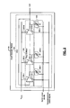
- FIG. 1A is a functional block diagram of a computing device according to the present disclosure
- FIG. 1B is a functional block diagram of a computing device according to the present disclosure.
- FIG. 2 is a functional block diagram of a voltage controlled oscillator (VCO) according to the present disclosure
- FIG. 3A is a functional block diagram of a power management module according to the present disclosure.
- FIG. 3B is a schematic of a switched capacitor bank according to the present disclosure.
- FIG. 4 depicts VCO frequency control as a function of processor speed demand according to the present disclosure
- FIG. 5 is a functional block diagram of a clock gating system according to the present disclosure.
- FIG. 6 is a flowchart of a method for controlling clock frequency of a processor according to the present disclosure.
- the speed of a processor depends on the frequency of a clock signal (clock frequency) supplied to the processor.
- the present disclosure relates to a voltage controlled oscillator (VCO) that generates the clock signal supplied to the processor.
- VCO voltage controlled oscillator
- the VCO adjusts the clock frequency according to the needs of an application being executed by the processor.
- the VCO adjusts the clock frequency based on the power consumption and/or voltage drop of a monitored device.
- the VCO adjusts the clock frequency by varying the transconductance of amplifiers (e.g., inverters) used in the VCO.
- the transconductance of amplifiers is varied by supplying one or more controlled inputs to the VCO.
- the controlled inputs include a power supply voltage of the VCO, an output of a digital-to-analog converter (DAC), and/or an input to a switched capacitor bank used in the VCO.
- the clock frequency may also be controlled using a clock gating system driven by a numerically controlled digital oscillator (NCO) as explained below.
- the transconductance of the amplifiers may be initially varied by adjusting a supply voltage of the amplifiers.
- the supply voltage is adjusted within a predetermined range having a maximum value and a minimum value.
- the output of the DAC and/or the input to the switched capacitor bank can be used to further vary the transconductance of the amplifiers.
- the clock frequency may be controlled using the clock gating system driven by the NCO.
- the computing device 100 includes a CPU 102 .
- the CPU 102 executes a software application 104 .
- a clock generator module 106 supplies a clock signal (CLK) having a clock frequency to the CPU 102 .
- CLK clock signal
- the CPU 102 executes the software application 104 at a speed determined by the clock frequency.
- a power management module 108 manages the power consumption of the CPU 102 by controlling the clock frequency.
- the clock generator module 106 generates the clock signal according to the controlled inputs supplied by the power management module 108 .
- An activity monitoring module 110 monitors activity of the CPU 102 .
- the activity monitoring module 110 collects statistical data about the activities of the CPU 102 .
- the power management module 108 receives an input indicating the activity level of the CPU 102 from the activity monitoring module 110 . Based on the input, the power management module 108 determines whether the speed of the CPU 102 can be reduced or needs to be increased. Accordingly, the power management module 108 automatically reduces or increases the speed of the CPU 102 by decreasing or increasing the clock frequency.
- the software application 104 can override the clock frequency set by the power management module 108 .
- the software application 104 can override the clock frequency set by the power management module 108 by writing a value to a register 112 that increases or decreases the clock frequency by jumping to a new target value.
- the software application 104 may override the clock frequency set by the power management module 108 when a portion of the code needs to run faster or when the software application 104 knows ahead of time that the software application 104 can slow down.
- the change in the clock frequency will have to be completed before the clock frequency can throttle down again automatically in response to a low activity rate of the CPU 102 .
- the reduction in the clock frequency can be negated after a predetermined time period if the power management module 108 senses that the CPU 102 is too busy at the lowered clock frequency.
- the clock frequency adjustment techniques disclosed herein may be similarly applied to a computing device 120 .
- the computing device 120 includes one or more circuit module(s) 122 , the power management module 108 and the clock generator module 106 .
- the circuit module(s) 122 provide power consumption and/or voltage information to the power management module 108 .
- the power management module 108 uses such information to provide the proper controlled inputs to the clock generator module 106 .
- the clock generator module 106 provides the appropriate clock signal to the circuit module(s) 122 .
- the clock frequency of the clock signal may be adjusted in a number of ways to account for various scenarios.
- the power consumption and/or voltage information relates to a supply voltage for powering the circuit module(s) 122 .
- the power management module 108 monitors the power or voltage level of the supply voltage and reduces the clock frequency accordingly in order to prevent operational failure(s) due to insufficient power or power glitches.
- Operational failure(s) may happen when the circuit module(s) 122 collectively demand more power than is available, such as, when the circuit module(s) 122 collectively and/or simultaneously engage in high activity levels. Such over-demand for power usually results in a sudden voltage drop or variation in the supply voltage.
- one or more of the circuit module(s) 122 may fail. Operational failure(s) may also happen when the circuit module(s) 122 engage in clock gating activities (such as powering or de-powering some or all of the circuit module(s) 122 ) which can result in power variations or glitches.
- the power management module 108 may respond to the voltage drop or variation by directing the clock generator module 106 to lower the clock frequency which, in turn, reduces the activity levels of the circuit module(s) 122 , thus minimizing operational failure(s) due to over-demand of power or power glitches.
- the computing device 120 would have to be designed to provide adequate built-in margin of error to accommodate worst case scenarios, which typically result in design and/or operational inefficiencies.
- the built-in margin of error may be minimized, thereby resulting in more efficient design and operations.
- the circuit modules 122 provide to the power management module 108 power consumption and/or voltage information relating to the level of consumption by the circuit modules 122 . If the power management module 108 determines that the level of consumption has increased (e.g., a voltage increase), which would mean that the activity levels of the circuit modules 122 have also increased, the power management module 108 then directs the clock generator module 106 to increase the clock frequency of the clock signal, thereby accommodating the increased levels of activity of the circuit modules 122 .
- the level of consumption e.g., a voltage increase
- the computing device 120 includes an end user device, such as, a mobile phone, a tablet, a laptop or the like and the circuit modules 122 include one or more integrated circuits (ICs) or chips.
- the computing device 120 includes a system-on-chip (SoC) and the circuit modules 122 include one or more circuit components.
- SoC system-on-chip
- the clock generator module 106 includes a voltage controlled oscillator (VCO) 200 that generates the clock signal.
- the VCO 200 includes a ring oscillator 202 and a switched capacitor bank 204 .
- the ring oscillator 202 includes a plurality of inverters 206 - 1 , 206 - 2 , . . . , and 206 -N (collectively inverters 206 ), where N is an integer greater than 1.
- the inverters 206 are connected in series. An output of a last inverter 206 -N is fed back to an input of a first inverter 206 - 1 .
- Other types of amplifiers may be used instead of the inverters 206 .
- the switched capacitor bank 204 includes a plurality of variable capacitors C 1 208 - 1 , C 2 208 - 2 , . . . , and Cn 208 - n (collectively variable capacitors 208 ), where n is an integer greater than 1.
- Each variable capacitor 208 may include a plurality of capacitors and a plurality of switches.
- the switches may include transistors.
- the plurality of capacitors and the plurality of switches can be arranged in different configurations. Some examples of the configurations are shown in FIG. 3B .
- a variable capacitor 208 is connected across an output of each inverter 206 and a common reference potential (e.g., ground).
- the clock frequency of the VCO 200 can be changed by changing the transconductance of the inverters 206 .
- the transconductance of the inverters 206 can be changed by supplying one or more of a plurality of controlled inputs to the VCO 200 as explained below.
- Each inverter 206 may include a transconductance control input 210 .
- the inverter 206 - 1 may include an input 210 - 1 ;
- the inverter 206 - 2 may include an input 210 - 2 ; and so on.
- the transconductance of an inverter 206 can be changed by supplying a transconductance control signal to the transconductance control input 210 of the inverter 206 .
- the switched capacitor bank 204 allows preset control of the transconductance.
- the switched capacitor bank 204 can also provide compensation for process variation.
- the ring oscillator 202 is responsive to a plurality of controlled inputs.
- the controlled inputs include a supply voltage V supply of the ring oscillator 202 , an output of a high-resolution DAC (see FIG. 3A ) including transconductance control signals supplied to the inputs 210 of the inverters 206 , and a set of control signals including switch control signals supplied to the variable capacitors 208 to control the switches (see FIG. 3B ).
- the clock frequency can be changed by changing one or more of the controlled inputs.
- the supply voltage of the inverters 206 is initially varied until the supply voltage reaches a minimum or maximum value of a predetermined range. Subsequently, one or more of the other controlled inputs (e.g., the transconductance control signals and/or the switch control signals) are utilized to change the clock frequency.
- the other controlled inputs e.g., the transconductance control signals and/or the switch control signals
- the supply voltage V supply of the ring oscillator 202 may be normally tied to a supply voltage of the CPU 102 (e.g., V dd ).
- the supply voltage V supply of the ring oscillator 202 can also be switched to an internally regulated voltage during calibration. Varying the supply voltage V supply of the ring oscillator 202 varies the transconductance of the inverters 206 of the ring oscillator 202 .
- the clock frequency can be changed by changing the supply voltage V supply within a predetermined range (e.g., V ddmin to V ddmax ).
- a predetermined range e.g., V ddmin to V ddmax
- the output of the DAC can be used to vary the transconductance of each of the inverters 206 .
- the switch control signals can be used to change the values of the variable capacitors 208 at the outputs of the inverters 206 . Varying the capacitors 208 at the outputs of the inverters 206 varies the transconductance of the inverters 206 .
- the ring oscillator 202 is used to implement the VCO 200 . It should be noted that, based on the disclosure and teaching provided herein, an LC oscillator and other types of oscillators may also be used to implement the VCO 200 .
- the power management module 108 includes memory 300 and a frequency adjustment module 303 .
- the frequency adjustment module 303 adjusts the clock frequency by generating one or more of the controlled inputs supplied to the VCO 200 .
- the frequency adjustment module 303 includes a DAC 304 , a capacitor switching module 306 , and a supply voltage control module 308 .
- the memory 300 may include a one-time programmable (OTP) nonvolatile memory (NVM) 301 and a plurality of registers 302 .
- OTP NVM 301 and the registers 302 store data used to generate one or more of the controlled inputs supplied to the VCO 200 .
- the data may be loaded during initialization (power up) and may be changed based on CPU activity.
- the DAC 304 and the capacitor switching module 306 use the data to generate the respective controlled inputs for the VCO 200 .
- the DAC 304 can use the data to generate the transconductance control signals supplied to the inputs 210 of the inverters 206 to control the transconductance of the inverters 206 .
- the capacitor switching module 306 can use the data to generate the switch control signals used to control the switches in the switched capacitor bank 204 .
- the supply voltage control module 308 can use the data to generate the control input V supply to adjust the supply voltage of the VCO 200 within the predetermined range (e.g., V ddmin to V ddmax ).
- each variable capacitor 208 may include a plurality of capacitors and a plurality of switches.
- the capacitors and switches may be arranged in different ways.
- capacitors C 1 , C 2 , . . . , and Cn may be respectively connected in series to switches S 1 , S 2 , . . . , and Sn, where n is an integer greater than 1.
- the series combinations of the capacitors and switches are connected in parallel as shown.
- capacitors C 1 , C 2 , . . . , and Cn are connected in series; and switches S 1 , S 2 , . . .
- the switches S 1 , S 2 , . . . , and Sn are connected across the capacitors C 1 , C 2 , . . . , and Cn, respectively.
- the switches S 1 , S 2 , . . . , and Sn can be controlled by the switch control signals.
- the value of the variable capacitors 208 at the output of each inverter 206 can be varied.
- the VCO 200 initializes at power up. Default values to initialize settings to generate the transconductance control signals and the switch control signals can be loaded into the plurality of registers 302 at power up. Alternatively, a time calibration of the VCO 200 can be performed using an automated test equipment (ATE) during manufacture.
- the one-time programmable (OTP) nonvolatile memory (NVM) 301 may be programmed with calibrated values used to supply preset transconductance control signals and switch control signals at power up.
- OTP one-time programmable nonvolatile memory
- the calibrated values for the transconductance control signals and the switch control signals may be loaded into the plurality of registers 302 from the OTP NVM 301 .
- the calibrated values can override the default values.
- the initial setup of the VCO 200 can generate a clock signal that meets setup time requirements of the CPU 102 within a supported V dd and temperature range. Deliberate CPU speed change at a higher frequency range relies mainly on V dd changes. Temperature changes, while related to system activities, may be considered independent since the relationship between the system activities and temperature changes may be too complex to predict. Uncontrolled V dd changes through dynamic or other systematic voltage drops are taken into account by directly affecting the clock frequency.
- An activity metric that measures an amount of CPU activity (or inactivity) may be used to control the VCO frequency.
- the activity monitoring module 110 can monitor idle state of the CPU 102 .
- a Wait-For-Interrupt (WFI) instruction can be used to indicate the idle state of the CPU 102 .
- a simple criterion to decide if the CPU 102 has more than a predetermined number of idle states is to count the number of WFI states within a predetermined period. For example, suppose the predetermined period is 1024 clock cycles. Within this predetermined period, suppose the activity monitoring module 110 senses more than say 20 WFI states. The power management module 108 can determine that the CPU 102 is idling a lot, that the clock frequency is too high, and that the clock frequency can be reduced.
- the power management module 108 can determine that the CPU 102 is idling a little (i.e., the CPU 102 is too busy), that the clock frequency is not too high, and that the clock frequency can be increased. If the number of WFI states within the predetermined period is between 10 and 20, the power management module 108 can keep the clock frequency unchanged.
- the power management module 108 can control the clock frequency by defining parameters such as IdleCountInterval, SpeedUpThreshold, and SlowDownThreshold.
- IdleCountInterval was 1024 clock cycles
- SpeedUpThreshold was greater than or equal to 20 WFI states
- SlowDownThreshold was less than or equal to 10 WFI states.
- the power management module 108 can use a parameter SlowDownHysterysis to avoid an invalid definition where the SpeedUpThreshold and the SlowDownThreshold cross each other.
- the power management module 108 may use a state machine to control the speed of the CPU 102 .
- the state machine can speed up or slow down the CPU 102 (i.e., increase or decrease the clock frequency of the VCO 200 ).
- the clock frequency of the VCO 200 is changed first by adjusting the supply voltage V dd of the CPU 102 .
- the supply voltage V dd is between a predetermined minimum value V ddmin and a predetermined maximum value V ddmax
- the clock frequency of the VCO 200 is controlled by adjusting the supply voltage V dd (e.g., from an external power management integrated circuit).
- any slowdown of the VCO 200 can be performed by adjusting the transconductance control signals of the VCO 200 .
- the frequency of the VCO 200 can be decreased by a programmable setting (e.g., about 20%) defined by a minimum value used by the DAC 304 to generate the transconductance control signals, say FineControlMin.
- the clock frequency of the VCO 200 can also be reduced from F minv to F minv1 by using the switch control signals.
- the switch control signals will have to be used if the inverters 206 do not include the transconductance control inputs 210 (e.g., if the ring oscillator components are based on simple digital inverters). If the inverters 206 include the transconductance control inputs 210 , the switch control signals are mainly used to adjust the variable capacitors 208 to compensate for process variation.
- the clock frequency of the VCO 200 can be controlled within a finite range using the transconductance control signals. In some applications, the CPU speed needs to be lowered further when the system does not need a lot of CPU resources.
- the clock frequency of the VCO 200 can be reduced below F minv1 by changing the capacitance of the variable capacitors 208 using the switch control signals. Alternatively, the clock frequency of the VCO 200 can be reduced below F minv1 by using clock gating control on the output of the VCO 200 .
- clock gating control can be used to reduce power consumption without encroaching on CPU setup time requirements.
- the clock gating logic can provide a large frequency adjustment range of say more than 1:1/100, for example.
- the clock gating logic can use a numerically control digital oscillator (NCO) having sufficient resolution to provide the large frequency adjustment range.
- the system 400 includes the CPU 102 , the power management module 108 , the VCO 200 , an NCO module 402 , and a clock gating module 404 .
- the power management module 108 controls the NCO module 402 .
- the NCO module 402 varies the clock frequency beyond the frequency range handled by the controlled inputs V supply , the transconductance control signals, and the switch control signals.
- the clock gating module 404 gates the clock signal to the CPU 102 according to the output of the NCO module 402 .
- the system 400 can provide a frequency adjustment range of 1:1/256 as follows.
- F minv1 1 GHz
- IdleCountInterval 16384 (16.4 us @ 1 GHz)
- the NCO has a resolution of 8 bits (i.e., 256 levels) and 6 bits fractional.
- the power management module 108 reduces the clock frequency to 1 GHz using one or more of the controlled inputs (e.g., by adjusting the supply voltage of the VCO 200 to V ddmin ).
- the activity monitoring module 110 counts the number of CPU WFI states during 16384 clock cycles and indicates to the power management module 108 whether the number of CPU WFI states is ⁇ 10 (SpeedUpThreshold) or >20 (SlowDownThreshold), for example.
- the power management module 108 outputs 8-bits to the NCO module 402 to update (increase or decrease) an NCO frequency.
- the interval selected is the longest interval used in the previous (1:1/16) range.
- the clock frequency can be changed from 1 ⁇ to 1/256 ⁇ in less than 10 ms.
- Ranges other than those described in the above example may be used. Additional or fewer ranges than those described in the above example may be used. System performance can be further improved if a rate of increasing the clock frequency is greater than a rate of decreasing the clock frequency. Accordingly, the power management module 108 may select a per-step increment value to input to the NCO module 402 to be larger than a per-step decrement value to input to the NCO module 402 .
- control monitors CPU activity during a predetermined period.
- control compares the CPU activity to a speed-up threshold or a slowdown threshold.
- control determines, based on the comparison, whether the clock frequency needs to be changed. Control returns to 502 if, based on the comparison, control determines that the clock frequency of the CPU does not need to be changed.
- control determines whether the clock frequency is below a predetermined value (e.g., less than 20% of a maximum value).
- a predetermined value e.g., less than 20% of a maximum value.
- control changes the transconductance of the amplifiers used in the VCO by changing the supply voltage, transconductance control inputs, and/or capacitance at the outputs of the amplifiers to change the clock frequency.
- Control returns to 502 .
- control changes the clock frequency using an NCO-driven clock gating system. Control returns to 502 .
- module may refer to, be part of, or include an Application Specific Integrated Circuit (ASIC); an electronic circuit; a combinational logic circuit; a field programmable gate array (FPGA); a processor (shared, dedicated, or group) that executes code; other suitable hardware components that provide the described functionality; or a combination of some or all of the above, such as in a system-on-chip.
- ASIC Application Specific Integrated Circuit
- FPGA field programmable gate array
- the term module may include memory (shared, dedicated, or group) that stores code executed by the processor.
- code may include software, firmware, and/or microcode, and may refer to programs, routines, functions, classes, and/or objects.
- shared means that some or all code from multiple modules may be executed using a single (shared) processor. In addition, some or all code from multiple modules may be stored by a single (shared) memory.
- group means that some or all code from a single module may be executed using a group of processors. In addition, some or all code from a single module may be stored using a group of memories.
- the apparatuses and methods described herein may be partially or fully implemented by one or more computer programs executed by one or more processors.
- the computer programs include processor-executable instructions that are stored on at least one non-transitory tangible computer readable medium.
- the computer programs may also include and/or rely on stored data.
- Non-limiting examples of the non-transitory tangible computer readable medium include nonvolatile memory, volatile memory, magnetic storage, and optical storage.
Landscapes
- Engineering & Computer Science (AREA)
- Theoretical Computer Science (AREA)
- Physics & Mathematics (AREA)
- General Engineering & Computer Science (AREA)
- General Physics & Mathematics (AREA)
- Power Sources (AREA)
- Inductance-Capacitance Distribution Constants And Capacitance-Resistance Oscillators (AREA)
Abstract
Description
Claims (18)
Priority Applications (2)
| Application Number | Priority Date | Filing Date | Title |
|---|---|---|---|
| US13/681,737 US8937511B2 (en) | 2011-11-22 | 2012-11-20 | Frequency scaling of variable speed systems for fast response and power reduction |
| PCT/US2012/066257 WO2013078311A1 (en) | 2011-11-22 | 2012-11-21 | Frequency scaling of variable speed systems for fast response and power reduction |
Applications Claiming Priority (2)
| Application Number | Priority Date | Filing Date | Title |
|---|---|---|---|
| US201161562666P | 2011-11-22 | 2011-11-22 | |
| US13/681,737 US8937511B2 (en) | 2011-11-22 | 2012-11-20 | Frequency scaling of variable speed systems for fast response and power reduction |
Publications (2)
| Publication Number | Publication Date |
|---|---|
| US20130127550A1 US20130127550A1 (en) | 2013-05-23 |
| US8937511B2 true US8937511B2 (en) | 2015-01-20 |
Family
ID=48426202
Family Applications (1)
| Application Number | Title | Priority Date | Filing Date |
|---|---|---|---|
| US13/681,737 Expired - Fee Related US8937511B2 (en) | 2011-11-22 | 2012-11-20 | Frequency scaling of variable speed systems for fast response and power reduction |
Country Status (2)
| Country | Link |
|---|---|
| US (1) | US8937511B2 (en) |
| WO (1) | WO2013078311A1 (en) |
Families Citing this family (7)
| Publication number | Priority date | Publication date | Assignee | Title |
|---|---|---|---|---|
| US9098280B2 (en) * | 2012-12-28 | 2015-08-04 | Intel Corporation | Staged power distribution control |
| US9513688B2 (en) | 2013-03-16 | 2016-12-06 | Intel Corporation | Measurement of performance scalability in a microprocessor |
| WO2015038478A1 (en) * | 2013-09-13 | 2015-03-19 | Marvell World Trade Ltd. | Dynamic clock regulation |
| US9778676B2 (en) * | 2015-08-03 | 2017-10-03 | Qualcomm Incorporated | Power distribution network (PDN) droop/overshoot mitigation in dynamic frequency scaling |
| US9798376B2 (en) * | 2015-08-03 | 2017-10-24 | Qualcomm Incorporated | Power distribution network (PDN) droop/overshoot mitigation |
| US10642336B2 (en) | 2016-07-12 | 2020-05-05 | Advanced Micro Devices, Inc. | Clock adjustment for voltage droop |
| US10303200B2 (en) | 2017-02-24 | 2019-05-28 | Advanced Micro Devices, Inc. | Clock divider device and methods thereof |
Citations (8)
| Publication number | Priority date | Publication date | Assignee | Title |
|---|---|---|---|---|
| US5343170A (en) | 1992-01-08 | 1994-08-30 | Samsung Electronics Co., Ltd. | Voltage controlled oscillator provided with negative feedback biasing |
| US6075419A (en) | 1999-01-29 | 2000-06-13 | Pmc-Sierra Ltd. | High speed wide tuning range multi-phase output ring oscillator |
| US20030229816A1 (en) * | 2002-02-25 | 2003-12-11 | Olivier Meynard | Clock control arrangement for a computing system, power management system and processing unit including the same |
| US7469355B1 (en) * | 2004-10-26 | 2008-12-23 | Nvidia Corporation | Auto tune dynamic over clocking |
| US20100156544A1 (en) | 2008-12-22 | 2010-06-24 | Electronics And Telecommunications Research Institute | Ring oscillator having wide frequency range |
| US7802118B1 (en) | 2006-12-21 | 2010-09-21 | Nvidia Corporation | Functional block level clock-gating within a graphics processor |
| US8044729B2 (en) * | 2009-10-09 | 2011-10-25 | Phison Electronics Corp. | Phase locked loop and voltage controlled oscillator thereof |
| US8373511B2 (en) * | 2010-10-15 | 2013-02-12 | Texas Instruments Incorporated | Oscillator circuit and method for gain and phase noise control |
-
2012
- 2012-11-20 US US13/681,737 patent/US8937511B2/en not_active Expired - Fee Related
- 2012-11-21 WO PCT/US2012/066257 patent/WO2013078311A1/en not_active Ceased
Patent Citations (8)
| Publication number | Priority date | Publication date | Assignee | Title |
|---|---|---|---|---|
| US5343170A (en) | 1992-01-08 | 1994-08-30 | Samsung Electronics Co., Ltd. | Voltage controlled oscillator provided with negative feedback biasing |
| US6075419A (en) | 1999-01-29 | 2000-06-13 | Pmc-Sierra Ltd. | High speed wide tuning range multi-phase output ring oscillator |
| US20030229816A1 (en) * | 2002-02-25 | 2003-12-11 | Olivier Meynard | Clock control arrangement for a computing system, power management system and processing unit including the same |
| US7469355B1 (en) * | 2004-10-26 | 2008-12-23 | Nvidia Corporation | Auto tune dynamic over clocking |
| US7802118B1 (en) | 2006-12-21 | 2010-09-21 | Nvidia Corporation | Functional block level clock-gating within a graphics processor |
| US20100156544A1 (en) | 2008-12-22 | 2010-06-24 | Electronics And Telecommunications Research Institute | Ring oscillator having wide frequency range |
| US8044729B2 (en) * | 2009-10-09 | 2011-10-25 | Phison Electronics Corp. | Phase locked loop and voltage controlled oscillator thereof |
| US8373511B2 (en) * | 2010-10-15 | 2013-02-12 | Texas Instruments Incorporated | Oscillator circuit and method for gain and phase noise control |
Non-Patent Citations (3)
| Title |
|---|
| ARM Limited: Cortex-AB Technical Reference Manual-Revision r2p3-Chapter 10; Oct. 6, 2008; 39 pages. |
| ARM Limited: Cortex-AB Technical Reference Manual—Revision r2p3—Chapter 10; Oct. 6, 2008; 39 pages. |
| PCT International Search Report for related PCT Application No. PCT/US2012/066257; Apr. 3, 2013; 5 pages. |
Also Published As
| Publication number | Publication date |
|---|---|
| WO2013078311A1 (en) | 2013-05-30 |
| US20130127550A1 (en) | 2013-05-23 |
| WO2013078311A4 (en) | 2013-07-18 |
Similar Documents
| Publication | Publication Date | Title |
|---|---|---|
| US8937511B2 (en) | Frequency scaling of variable speed systems for fast response and power reduction | |
| US9383789B2 (en) | Thermal control apparatus and methodology | |
| CN110908488B (en) | Voltage drop monitoring circuit and system on chip | |
| US8442697B2 (en) | Method and apparatus for on-demand power management | |
| KR102190453B1 (en) | Power management device and system on chip including the same | |
| US20120117402A1 (en) | Memory Read Timing Margin Adjustment | |
| US20080059817A1 (en) | Processor system | |
| KR102340679B1 (en) | Clock adjustment for voltage droop | |
| CN106415521B (en) | Hardware device and method for multiprocessing dynamic asymmetric and symmetric mode switching | |
| US10147464B1 (en) | Managing power state in one power domain based on power states in another power domain | |
| JP2016511485A (en) | Digital Assisted Adjustment for Integrated Capless Low Dropout (LDO) Voltage Regulator | |
| US9413361B1 (en) | Closed loop clock signal generator with multiple reference clocks | |
| US9395775B2 (en) | Control scheme to temporarily raise supply voltage in response to sudden change in current demand | |
| US10572266B2 (en) | Systems, methods, and apparatus for controlling the power-on or boot sequence of an integrated circuit based on power harvesting conditions | |
| US11942953B2 (en) | Droop detection and control of digital frequency-locked loop | |
| US9246496B2 (en) | Semiconductor device, semiconductor system and method for operating semiconductor device | |
| WO2019067262A1 (en) | Voltage regulator including switching frequency self-optimization | |
| US9292301B1 (en) | Systems, methods, and apparatus for controlling the power-on or boot sequence of an integrated circuit based on power harvesting conditions | |
| US10915257B2 (en) | Semiconductor device and semiconductor system | |
| US6999354B2 (en) | Dynamically adaptable memory | |
| US12278638B2 (en) | Droop detection and control of digital frequency-locked loop | |
| US20200192448A1 (en) | Control circuit and method for fast setting power mode | |
| KR20160131182A (en) | Integrated circuit and computing device having the same | |
| De | Energy efficient computing in nanoscale CMOS: Challenges and opportunities |
Legal Events
| Date | Code | Title | Description |
|---|---|---|---|
| AS | Assignment |
Owner name: MARVELL INTERNATIONAL LTD., BERMUDA Free format text: LICENSE;ASSIGNOR:MARVELL WORLD TRADE LTD.;REEL/FRAME:029350/0425 Effective date: 20121126 Owner name: MARVELL INTERNATIONAL LTD., BERMUDA Free format text: ASSIGNMENT OF ASSIGNORS INTEREST;ASSIGNOR:MARVELL SEMICONDUCTOR, INC.;REEL/FRAME:029350/0347 Effective date: 20121119 Owner name: MARVELL WORLD TRADE LTD, BARBADOS Free format text: ASSIGNMENT OF ASSIGNORS INTEREST;ASSIGNOR:MARVELL INTERNATIONAL LTD.;REEL/FRAME:029350/0399 Effective date: 20121119 Owner name: MARVELL SEMICONDUCTOR, INC., CALIFORNIA Free format text: ASSIGNMENT OF ASSIGNORS INTEREST;ASSIGNORS:SUTARDJA, PANTAS;SUTARDJA, SEHAT;SIGNING DATES FROM 20121031 TO 20121116;REEL/FRAME:029350/0287 |
|
| STCF | Information on status: patent grant |
Free format text: PATENTED CASE |
|
| MAFP | Maintenance fee payment |
Free format text: PAYMENT OF MAINTENANCE FEE, 4TH YEAR, LARGE ENTITY (ORIGINAL EVENT CODE: M1551) Year of fee payment: 4 |
|
| AS | Assignment |
Owner name: MARVELL INTERNATIONAL LTD., BERMUDA Free format text: ASSIGNMENT OF ASSIGNORS INTEREST;ASSIGNOR:MARVELL WORLD TRADE LTD.;REEL/FRAME:051778/0537 Effective date: 20191231 |
|
| AS | Assignment |
Owner name: CAVIUM INTERNATIONAL, CAYMAN ISLANDS Free format text: ASSIGNMENT OF ASSIGNORS INTEREST;ASSIGNOR:MARVELL INTERNATIONAL LTD.;REEL/FRAME:052918/0001 Effective date: 20191231 |
|
| AS | Assignment |
Owner name: MARVELL ASIA PTE, LTD., SINGAPORE Free format text: ASSIGNMENT OF ASSIGNORS INTEREST;ASSIGNOR:CAVIUM INTERNATIONAL;REEL/FRAME:053475/0001 Effective date: 20191231 |
|
| FEPP | Fee payment procedure |
Free format text: MAINTENANCE FEE REMINDER MAILED (ORIGINAL EVENT CODE: REM.); ENTITY STATUS OF PATENT OWNER: LARGE ENTITY |
|
| LAPS | Lapse for failure to pay maintenance fees |
Free format text: PATENT EXPIRED FOR FAILURE TO PAY MAINTENANCE FEES (ORIGINAL EVENT CODE: EXP.); ENTITY STATUS OF PATENT OWNER: LARGE ENTITY |
|
| STCH | Information on status: patent discontinuation |
Free format text: PATENT EXPIRED DUE TO NONPAYMENT OF MAINTENANCE FEES UNDER 37 CFR 1.362 |
|
| FP | Lapsed due to failure to pay maintenance fee |
Effective date: 20230120 |