US8933727B1 - Monolithic transmit/receive module driver - Google Patents
Monolithic transmit/receive module driver Download PDFInfo
- Publication number
- US8933727B1 US8933727B1 US13/592,816 US201213592816A US8933727B1 US 8933727 B1 US8933727 B1 US 8933727B1 US 201213592816 A US201213592816 A US 201213592816A US 8933727 B1 US8933727 B1 US 8933727B1
- Authority
- US
- United States
- Prior art keywords
- control signal
- transmit
- receive
- circuit
- outputs
- Prior art date
- Legal status (The legal status is an assumption and is not a legal conclusion. Google has not performed a legal analysis and makes no representation as to the accuracy of the status listed.)
- Active, expires
Links
Images


Classifications
-
- H—ELECTRICITY
- H03—ELECTRONIC CIRCUITRY
- H03K—PULSE TECHNIQUE
- H03K19/00—Logic circuits, i.e. having at least two inputs acting on one output; Inverting circuits
- H03K19/0175—Coupling arrangements; Interface arrangements
- H03K19/017509—Interface arrangements
-
- G—PHYSICS
- G01—MEASURING; TESTING
- G01S—RADIO DIRECTION-FINDING; RADIO NAVIGATION; DETERMINING DISTANCE OR VELOCITY BY USE OF RADIO WAVES; LOCATING OR PRESENCE-DETECTING BY USE OF THE REFLECTION OR RERADIATION OF RADIO WAVES; ANALOGOUS ARRANGEMENTS USING OTHER WAVES
- G01S7/00—Details of systems according to groups G01S13/00, G01S15/00, G01S17/00
- G01S7/02—Details of systems according to groups G01S13/00, G01S15/00, G01S17/00 of systems according to group G01S13/00
- G01S7/03—Details of HF subsystems specially adapted therefor, e.g. common to transmitter and receiver
- G01S7/032—Constructional details for solid-state radar subsystems
Definitions
- the present invention relates to radar systems generally and, more particularly, to a method and/or apparatus for implementing a monolithic transmit/receive (T/R) module driver.
- T/R transmit/receive
- T/R Transmit/receive
- Typical T/R modules can include power amplifier (PA) stages, low noise amplifier (LNA) stages, digital phase shifters, digital attenuators and T/R switches for interconnecting various components depending on whether the T/R module is in a transmit or a receive mode.
- PA power amplifier
- LNA low noise amplifier
- T/R switches for interconnecting various components depending on whether the T/R module is in a transmit or a receive mode.
- Driving conventional T/R modules takes multiple drivers and discrete components.
- the present invention concerns an integrated circuit comprising a first circuit and a second circuit.
- the first circuit may be configured to generate a plurality of complementary outputs based upon a plurality of inputs, a first control signal, and a second control signal.
- the plurality of inputs may be received in parallel in a first mode and as a serial bit stream in a second mode.
- the second circuit may be configured to generate a plurality of outputs in response to a third control signal and a fourth control signal.
- T/R transmit/receive
- the objects, features and advantages of the present invention include providing a monolithic transmit/receive (T/R) module driver that may (i) reduce the number of drive signals, (ii) reduce the number of package pins needed, (iii) provide separate control of multiple amplifier stages to reduce potential feedback, and/or (iv) control transmitter and receiver amplifiers based on operating mode.
- T/R transmit/receive
- FIG. 1 is a diagram illustrating a transmit/receive module driver in accordance with an embodiment of the present invention
- FIG. 2 is a block diagram illustrating an example implementation of a transmit/receive (T/R) module driver in accordance with an embodiment of the present invention
- FIG. 3 is a diagram illustrating a functional schematic for one bit of a serial/parallel driver circuit of FIG. 2 ;
- FIG. 4 is a diagram illustrating an application circuit for controlling a T/R amplifier utilizing an open-drain NMOSFET output of the T/R module driver of FIG. 2 ;
- FIG. 5 is a diagram illustrating a package in which an integrated circuit implementing a T/R module driver in accordance with an embodiment of the present invention may be mounted;
- FIG. 6 is a timing diagram illustrating operation of a serial interface of a transmit/receive module driver in accordance with an embodiment of the present invention
- FIG. 7 is a timing diagram illustrating switching waveforms between an input interface and an output interface of a transmit/receive module driver in accordance with an embodiment the present invention.
- FIG. 8 is a diagram illustrating a transmit/receive module driver in accordance with a preferred embodiment of the present invention implemented in a radar system.
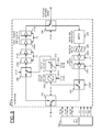
- the circuit 100 may implement a transmit/receive module driver.
- the circuit 100 may, in one example, be implemented as a dedicated complimentary metal oxide semiconductor (CMOS) driver for multifunction modules such as GaAs based transmit/receive modules.
- CMOS complementary metal oxide semiconductor
- the circuit 100 may be implemented on a monolithic integrated circuit (IC).
- the circuit 100 may be configured to accept transmit/receive and enable inputs, and translate the transmit/receive and enable inputs to control transmit/receive (T/R) switches in a transmit/receive (T/R) module and enable/disable transmit and receive amplifiers either separately or shutting off both transmit and receive amplifiers in a power conservation state.
- the circuit 100 may include a serial/parallel interface. In one example, a 6-bit serial/parallel interface may be implemented. However, other numbers of bits may be implemented accordingly to meet the design criteria of a particular implementation.
- the serial/parallel interface may be configured to drive digital attenuators and/or phase shifters.
- the circuit 100 may also include functionality to switch between transmit and receive channels and to enable/disable LNAs and/or PAs.
- high speed analog CMOS technology may be utilized in implementing the transmit/receive module driver 100 to achieve low power consumption at moderate to high speeds.
- the T/R module driver 100 may include an input 102 , an input 104 , an input 106 , an input 108 , an input 110 , an input 112 , an input 114 , an output 116 , an output 118 , an output 120 , an output 122 , an output 124 , an output 126 , an output 128 and an output 130 .
- the input 102 may receive a clock signal (e.g., CLK).
- the input 104 may receive a serial data stream (e.g., SER_IN).
- the input 106 may receive a signal (e.g., S/P).
- the signal S/P may implement a control signal for switching between a serial and parallel operating mode.
- the input 108 may provide a number (e.g., 6) of parallel inputs for receiving a number of input bits (e.g., C 1 -C 6 ).
- the input 110 may receive a signal (e.g., LE).
- the signal LE may implement a control signal that may be used to latch input data in the circuit 100 .
- the input 112 may receive a signal (e.g., EN).
- the signal EN may be implemented as a control signal that may be used to enable/disable circuitry attached to the circuit 100 .
- the input 114 may receive a signal (e.g., T/R).
- the signal T/R may be implemented as a control signal for switching between a transmit and a receive mode.
- the signals EN and T/R may be used to control logic configured to enable/disable low noise amplifiers (LNAs) and power amplifiers (PAs) attached to the circuit 100 .
- LNAs low noise amplifiers
- PAs power amplifiers
- the output 116 may present a serial output data stream (e.g., SER_OUT).
- the output 118 may present a first set of parallel outputs (e.g., A 1 -A 6 ).
- the output 120 may present a second set of parallel outputs (e.g., B 1 -B 6 ).
- the outputs B 1 -B 6 may be complementary to the outputs A 1 -A 6 .
- the output 122 may present a pair of complementary signals (e.g., A 7 and B 7 ).
- the output 124 may present a signal (e.g., L 1 ).
- the output 126 may present a signal (e.g., L 2 ).
- the output 128 may present a signal (e.g., P 1 ).
- the output 130 may present a signal (e.g., P 2 ).
- the signals L 1 , L 2 , P 1 and P 2 may be used, in one example, to control amplifiers in a T/R module being driven by the circuit 100 .
- the signals L 1 and L 2 may be used to control separate stages of a low noise amplifier (LNA) section.
- the signals P 1 and P 2 may be used to control separate stages of a power amplifier (PA) section.
- PA power amplifier
- the use of multiple control signals to control multiple amplifier stages may reduce the possibility of instability due to feedback between the amplifier stages.
- the circuit 100 may comprise a block 150 and a block 160 .
- the block 150 may implement a serial/parallel driver.
- the block 160 may implement a T/R control module.
- the serial/parallel driver 150 is generally implemented using the parallel input 108 (e.g., the signals C 1 -C 6 ), the mode control input 106 (e.g., the signal S/P), the parallel output 118 (e.g., the in phase outputs A 1 -A 6 ), the parallel output 120 (e.g., the complementary outputs B 1 -B 6 ) and the serial output 116 .
- a serial control interface is generally implemented with the input 102 (e.g., CLK), the input 104 (e.g., SER_IN), the input 110 (e.g., LE) and the serial output 116 (e.g., SER_OUT).
- the serial control interface may be compatible with SPI protocol.
- the serial control interface may be activated when the signal S/P is maintained at an asserted level (e.g., set to a logic HIGH, or 1).
- a serial word e.g., 6 bits
- the signal LE may be asserted (e.g., set to a logic HIGH, or 1) to latch (transfer) the data for presentation on the complementary outputs A 1 -A 6 and B 1 -B 6 .
- the signal CLK may be masked to prevent data transition during the data transfer.
- the signal SER_OUT generally comprises the signal SER_IN delayed by a number of clock cycles equivalent to the word size implemented (e.g., 6 clock cycles for a 6-bit word).
- the parallel mode is generally enabled when the signal S/P is maintained at a de-asserted level (e.g., set to a logic LOW, or 0). In the parallel mode, the outputs A 1 -A 6 and B 1 -B 6 may be controlled by the parallel inputs C 1 -C 6 directly.
- the T/R control module is generally implemented using the input 112 (e.g., the signal EN), the input 114 (e.g., the signal T/R), and the outputs 122 - 130 (e.g., the signals A 7 , B 7 , L 1 , L 2 , P 1 , P 2 ).
- the output signals A 7 and B 7 are generally configured to drive switches in a multi-function module connected to the circuit 100 .
- the signals A 7 and B 7 may be used to control single-pole double-throw (SPDT) T/R switches in a T/R module in order to switch between transmit and receive modes.
- the T/R control module may be further configured to use a combination of the input signals EN and T/R to implement power consumption control.
- the T/R control module may control the output signals L 1 , L 2 , P 1 and P 2 based upon the combination of the input signals EN and T/R.
- the output signals L 1 , L 2 , P 1 and P 2 may then be utilized to turn on/off subsequent circuitry.
- the signals L 1 , L 2 , P 1 and P 2 may be configured to turn on/off receive path LNAs and transmit path PAs in a T/R module.
- the signals L 1 , L 2 , P 1 and P 2 may be implemented with open-drain NMOS FETs. When the NMOS FETs are turned on, the NMOS FETs may pull down a gate of GaAs FETs in the amplifiers to shut the amplifiers down.
- the signals L 1 , L 2 , P 1 and P 2 may be used to control up to four LNA stages and four PA stages.
- the T/R control module 160 may include logic and/or a look-up table (LUT) implementing the following TABLE 1:
- the block 150 may comprise a block 151 , a block 153 , a block 155 , a block 157 , a block 159 .
- the block 160 may comprise a block 162 , a block 164 , a block 166 and a block 168 .
- the block 151 may be implemented, in one example, as a 6-bit shift register.
- the block 153 may be implemented, in one example, as a 6-bit input buffer.
- the block 155 may be implemented, in one example, as a G-bit latch.
- the block 157 may be implemented, in one example, as a voltage translator.
- the block 159 may be implemented, in one example, as an output buffer/inverter block.
- the block 162 may be implemented as a control logic.
- the block 164 may be implemented, in one example, as voltage translators.
- the block 166 may be implemented, in one example, as output buffers/inverters.
- the block 168 may be implemented, in one example, as a number of open drain NMOS field effect transistors.
- the block 151 may have a first input that may receive the signals CLK, a second input that may receive the signal SER_IN, a third input that may receive the signal S/P and a first output that may present the signal SER_OUT and a second output that may present parallel signals to a first input of the block 155 .
- the block 153 may have a first input that may receive the signals C 1 -C 6 and a second input that may receive the signal S/P.
- the block 153 may have an output that may present a number of bits to a second input of the block 155 .
- the block 155 may have a third input that may receive the signal LE and an output that may present a number of bits to an input of the block 157 .
- the block 157 may have an output that may present a number of signals to an input of the block 159 .
- the block 159 may have a number of first outputs that may present the signals A 1 -A 6 and a number of second outputs that may present the signals B 1 -B 6 .
- the block 162 may have a first input that may receive the signal EN and a second input that may receive the signal T/R. An output of the block 162 may be presented to an input of the block 164 .
- the block 152 may implement logic and/or a look-up table embodying the truth table of TABLE 1 above.
- the block 164 may have a first output that may present a number of signals to an input of the block 166 and a second output that may present a number of signals to an input of the block 168 .
- the block 166 may have a number of outputs that may present the signals A 7 and B 7 .
- the block 168 may have a number of outputs that may present the signals L 1 , L 2 , P 1 and P 2 .
- the circuit 180 generally represents a function schematic of a pathway by which the serial/parallel driver circuit 150 of FIG. 2 generates the signals A 1 -A 6 and B 1 -B 6 in response to the signals C 1 -C 6 .
- the circuit 180 generally comprises a block 182 , a block 184 , a block 186 , a block 188 , and a number of transistors T 1 -T 4 .
- the block 182 generally represents TTL (transistor transistor logic) circuitry that may, in one example, be used to implement the blocks 151 , 153 and 155 .
- the blocks 184 and 188 generally represent the voltage translator module 157 of the serial/parallel driver circuit 150 .
- the block 186 generally represents an inverter function that may be used to generate a complement of a signal.
- the transistors T 1 -T 4 generally represent the output buffer/inverter block 159 of the serial parallel driver circuit 150 .
- an input signal (e.g., CN) is presented to an input of the TTL portion of the circuit 182 .
- the TTL portion 182 generates an output that is presented to an input of the block 184 and an input of the block 186 .
- the block 184 generally shifts the received signal to a voltage level appropriate for driving the transistors T 1 and T 2 .
- the block 186 generally inverts (complements) the received signal and presents the complemented signal to an input of the block 188 .
- the block 188 generally shifts the received signal to a voltage level appropriate for driving the transistors T 3 and T 4 .
- the transistors T 1 and T 2 are generally configured to generate an output signal (e.g., AN) in response to a first supply voltage (e.g., VOPT) and a second supply voltage (e.g., VEE).
- the transistors T 3 and T 4 are configured to generate an output signal (e.g., BN) in response to the power supplies VOPT and VEE.
- the output signal AN generally tracks the input signal CN.
- the output BN is generally a complement of the input signal CN.
- Multiple instances of the circuit 180 may be implemented to generate the signals A 1 -A 6 and B 1 -B 6 in FIG. 2 .
- the serial/parallel driver circuit 150 is generally configured to translate logic level (e.g., TTL, CMOS, LVCMOS, etc.) control inputs into negative gate control voltages for gallium arsenide (GaAs) FET microwave switches, phase shifters, and attenuators.
- the serial/parallel driver circuit 150 may be implemented using high speed analog CMOS technology to achieve low power dissipation at moderate to high speeds.
- the serial/parallel driver circuit 150 may be implemented to encompass most microwave switching applications.
- the signals A 1 -A 7 and B 1 -B 7 may be implemented with an output HIGH level in the range of 0-2 volts relative to ground (CND).
- the range of 0-2 volts relative to ground may optimize the intermodulation products of GaAs FET control devices at low frequencies.
- one or more of the outputs A 1 -A 7 and B 2 -B 7 may be switched between +5 and ⁇ 5 volts.
- the voltage range implemented may be selected to meet the design criteria of a particular application.
- the actual driver output voltages may be lower when driving large currents due to resistance of the output devices (e.g., represented by the transistors T 1 -T 4 ).
- the voltage supply VOPT may be grounded when FETs are driven.
- the supply voltage VOPT may be set between 1.0 and 2.0 volts to improve the intermodulation performance and the 1 dB compression point of GaAs control devices at low frequencies.
- FIG. 4 a diagram is shown illustrating an application circuit that may be implemented to control a T/R amplifier utilizing one of the open-drain NMOSFETs 168 of the T/R control module 160 of FIG. 2 .
- the open-drain NMOSFETs of the module 168 generally provide the signals L 1 , L 2 , P 1 and P 2 presented at the outputs 124 - 130 of the T/R module driver 100 .
- the NMOSFETs When the open-drain NMOSFETs 168 are turned on, the NMOSFETs may be used, for example, to pull down a gate voltage of a GaAs FET in an amplifier of a T/R module (or other device) attached to the T/R module driver 100 to pinch off the GaAs FET.
- each of the output signals L 1 , L 2 , P 1 and/or P 2 may be generated by a corresponding open-drain NMOSFET 190 .
- the open-drain output may be connected to a voltage divider formed using a resistor R 1 and a resistor R 2 and connected between ground and a supply voltage (e.g., VEE).
- the voltage divider may be used to bias a gate of the GaAs FET in the device to be controlled when the open-drain NMOSFET 190 is not conducting (or turned off).
- the T/R module driver 100 may be implemented as a monolithic integrated circuit (UI) 195 .
- the monolithic integrated circuit 195 may be packaged in a 5 mm PQFN-40LN lead-free plastic package.
- the serial interface signals may share pins used by the parallel interface signals. Sharing pins between the serial and parallel interfaces generally reduces the overall number of pins needed for the integrated circuit.
- the serial control interface may be activated when the signal S/P is maintained at an asserted level (e.g., set to a logic HIGH, or 1).
- a serial word e.g., 6 bits
- SER_IN data bits contained in the signal SER_IN may be sampled on a rising edge of the signal CLK.
- the signal LE When the serial word has been loaded, the signal LE may be asserted (e.g., set to a logic HIGH, or 1) to latch (transfer) the data for presentation on the complementary outputs A 1 -A 6 and B 1 -B 6 .
- the signal CLK When the signal LE is asserted, the signal CLK may be masked to prevent data transition during the data transfer.
- the signal SER_OUT generally comprises the signal SER_IN delayed by a number of clock cycles equivalent to the word size implemented (e.g., 6 clock cycles for a 6-bit word).
- the parallel mode is generally enabled when the signal S/P is maintained at a de-asserted level (e.g., set to a logic LOW, or 0). In the parallel mode, the outputs A 1 -A 6 and B 1 -B 6 may be controlled by the parallel inputs C 1 -C 6 directly.
- the input signals C 1 -C 6 may swing between predefined logic levels (e.g., TTL, 3V, etc.).
- the output signals A 1 -A 7 and B 1 -B 7 may be configured to swing between a high output voltage level and a low output voltage level in response to the input signals.
- the output signals may swing between voltage levels other than the levels of the input signals.
- the output signals A 1 -A 7 and B 1 -B 7 may swing between GND as the high output voltage level and VEE as the low output voltage level.
- other voltage levels may be implemented accordingly to meet the design criteria of a particular implementation.
- FIG. 8 a diagram is shown illustrating a context in which a T/R module driver in accordance with an embodiment of the present invention may be implemented.
- the T/R module driver 100 may be connected with a T/R module 200 .
- the T/R module 200 may be part of a radar system.
- other RF transmit/receive systems e.g., cellular phone system, WiFi, etc.
- the T/R module 200 may comprise a module (or circuit) 202 , a module (or circuit) 204 , a module (or circuit) 206 , a module (or circuit) 208 , a module (or circuit) 210 , a module (or circuit) 212 , a number of modules (or circuits) 214 a - 214 n , a number of modules (or circuits) 216 a - 216 n , a module (or circuit) 218 , a module (or circuit) 220 , and a number of modules (or circuits) 222 a - 222 n .
- the modules 202 - 208 may be implemented as transmit/receive (T/R) switches.
- the module 210 may be implemented as a digital phase shifter.
- the module 212 may be implemented as a digital attenuator.
- the modules 214 a - 214 n may implement power amplifier (PA) stages of a transmit path of the T/R module 200 .
- the modules 216 a - 216 n may implement final power amplifier (PA) stages of the transmit path of the T/R module 200 .
- the module 218 may implement a limiter configured to provide protection for a receiver path of the T/R module 200 .
- the module 220 may implement a receive filter.
- the modules 222 a - 222 n may implement low noise amplifier (LNA) stages of the receive path of the T/R module 200 .
- LNA low noise amplifier
- the T/R module 200 may be configured to receive the signals A 1 -A 7 , B 1 -B 7 , L 1 , L 2 , P 1 , and P 2 from the T/R module driver 100 .
- the signals A 7 and B 7 may be used to control the T/R switch modules 202 , 204 , 206 and 208 to select between transmit and receive modes of the T/R module 200 .
- a unidirectional arrow is depicted in the T/R switch modules 202 , 204 , 206 and 208 , signals may flow in either direction, as is required to transmit and receive.
- the transmit path of the T/R module 200 generally begins at the T/R switch module 202 .
- an RF signal may flow across the T/R switch module 202 from an RF input/output connection to the T/R switch module 204 , and then to the module 210 .
- the RF signal may be phase shifted by the module 210 .
- the module 210 may implement a variable phase shifter.
- the module 210 may be configured to implement a number of bits (e.g., 3 ) of phase shift. However, other numbers of bits may be implemented accordingly to meet the design criteria of a particular implementation.
- the amount of phase shift may be determined, in one example, using the signals A 1 -A 3 and B 1 -B 3 .
- the RF signal may be attenuated by the module 212 .
- the module 212 may implement a variable resistance.
- the module 212 may be configured to implement a number of bits (e.g., 3) of attenuation.
- the amount of attenuation may be determined, in one example, using the signals A 4 -A 6 and B 4 -B 6 .
- other numbers of bits may be implemented accordingly to meet the design criteria of a particular implementation.
- the modules 210 and 212 may implement the same or a different number of bits. For example, fine grained phase shift and attenuation may be employed to make small adjustments to a shape of an RF signal transmitted by an antenna array connected to the T/R module 200 .
- the RF signal may exit the module 212 and continue to the power amplifier (PA) stages 214 a - 214 n and 216 a - 216 n via the module 206 .
- PA power amplifier
- the transmit path of the T/R module 200 may have four gain stages. However, other numbers of gain stages may be implemented accordingly to ensure that the transmitted signal has the requisite signal strength.
- the power amplifier stage 216 n outputs the amplified RF signal to the T/R switch module 208 , where the amplified RF signal is routed to an antenna or antenna array connected to the T/R module 200 .
- the T/R switch module 208 is generally implemented as a high power switch that connects the antenna or antenna array to either the transmit path or to the receive path of the T/R module 200 (e.g., generally determined by the signals A 7 and B 7 ). In one example, the T/R switch module 208 may be integrated with the final power amplifier stages 216 a - 216 n.
- the receive path of the T/R module 200 generally begins where the T/R switch module 208 connects to the lead from the antenna or antenna array. The receive path continues through the module 218 and the module 220 to the modules 222 a - 222 n .
- the module 218 generally limits the received RF signal to protect the receiver circuitry.
- the module 220 generally provides filtering of the received RF signal.
- the modules 222 a - 222 n generally provide a number of gain stages forming a low noise amplifier (LNA).
- LNA low noise amplifier
- a low noise amplifier (LNA) is generally used to amplify the RF signal received by the antenna array because these signals are often too weak to be directly fed into other circuit components.
- a LNA is a type of amplifier that is optimized to produce as little noise as possible while still meeting amplification requirements for the signal.
- An output of the module 222 n flows across the T/R switch module 204 to the module 210 .
- the modules 202 , 204 , 206 , 210 , and 212 generally perform the same function on the received signals as performed on the transmitted signals.
- a series of gain stages may be implemented in conjunction with the modules 210 and 212 .
- gain stages may be implemented before, between and/or after the modules 210 and 212 .
- the output of the module 212 may travel across the T/R switch module 206 to the T/R switch module 202 , and then to the RF input/output connection of the T/R module 200 .
- the signals L 1 , L 2 , P 1 , and/or P 2 may be used to reduce power dissipation of the T/R module 200 by disabling (e.g., shutting down) one or more of the power amplifier stages of the transmit path or the low noise amplifier stages of the receive path depending upon whether the T/R module is in the transmit or receive mode.
- the signal P 1 may be used to enable/disable the modules 214 a - 214 n
- the signal P 2 may be used to enable/disable the modules 216 a - 216 n
- the signal L 1 may be used to enable/disable the module 222 a
- the signal L 2 may be used to enable/disable the module 222 n .
- the signals L 1 and L 2 may be configured to control the operation of the low noise amplifier (LNA) stages 222 a - 222 n in the receive path to reduce power dissipation during operation of the T/R module 200 in the transmit mode.
- the signals P 1 and P 2 may be configured to control operation of the power amplifier (PA) stages 214 a - 214 n and 216 a - 216 n in the transmit path to reduce power dissipation during operation of the T/R module 200 in the receive mode.
- PA power amplifier
- Embodiments of the present invention may be used to implement transmit/receive (T/R) module drivers that may be used to drive conventional T/R modules as well as transmit/receive functions built with discrete devices.
- embodiments of the present invention may be used to implement transmit/receive (T/R) module drivers configured to control various switches, phase shifters, attentuators, amplifiers (or gain stages), etc. of various transmit/receive systems.
- the signals A 1 -A 6 and/or the signals B 1 -B 6 may be used to program sub-modules (e.g., phase shifters, attenuators, switches, etc.) of the transmit/receive systems.
- the signals L 1 , L 2 , P 1 and/or P 2 may be used to control the power to various sub-modules (e.g., amplifiers, etc.) of the transmit/receive systems.
- the signals A 7 and B 7 may be used to control transmit/receive switches of the transmit/receive systems. Additional signals may be implemented accordingly to meet the design criteria of a particular implementation.
- the term “simultaneously” is meant to describe events that share some common time period but the term is not meant to be limited to events that begin at the same point in time, end at the same point in time, or have the same duration.
Landscapes
- Engineering & Computer Science (AREA)
- Radar, Positioning & Navigation (AREA)
- Remote Sensing (AREA)
- Physics & Mathematics (AREA)
- Computer Networks & Wireless Communication (AREA)
- General Physics & Mathematics (AREA)
- Computer Hardware Design (AREA)
- Computing Systems (AREA)
- General Engineering & Computer Science (AREA)
- Mathematical Physics (AREA)
- Amplifiers (AREA)
Abstract
Description
| TABLE 1 | |||
| Inputs | Outputs | ||
| EN | T/R | A7 | B7 | L1, L2 | P1, | ||
| 0 | 1 | GND | VEE | Hi-Z | Hi- | ||
| 0 | 0 | VEE | GND | Hi-Z | Hi- | ||
| 1 | 1 | GND | VEE | Hi- | LOW | ||
| 1 | 0 | VEE | GND | LOW | Hi-Z | ||
The LOW state shown in the TABLE 1 generally refers to the NMOS FET being on (e.g., pulling the associated output to approximately VEE+0.1V). The Hi-Z state in the TABLE 1 generally refers to the open-drain FET being shut off and presenting a high impedance.
Claims (21)
Priority Applications (2)
| Application Number | Priority Date | Filing Date | Title |
|---|---|---|---|
| US13/592,816 US8933727B1 (en) | 2012-08-23 | 2012-08-23 | Monolithic transmit/receive module driver |
| US14/167,079 US9148144B1 (en) | 2012-08-23 | 2014-01-29 | Monolithic transmit/receive module driver including PIN driver |
Applications Claiming Priority (1)
| Application Number | Priority Date | Filing Date | Title |
|---|---|---|---|
| US13/592,816 US8933727B1 (en) | 2012-08-23 | 2012-08-23 | Monolithic transmit/receive module driver |
Related Child Applications (1)
| Application Number | Title | Priority Date | Filing Date |
|---|---|---|---|
| US14/167,079 Continuation-In-Part US9148144B1 (en) | 2012-08-23 | 2014-01-29 | Monolithic transmit/receive module driver including PIN driver |
Publications (1)
| Publication Number | Publication Date |
|---|---|
| US8933727B1 true US8933727B1 (en) | 2015-01-13 |
Family
ID=52247760
Family Applications (1)
| Application Number | Title | Priority Date | Filing Date |
|---|---|---|---|
| US13/592,816 Active 2033-04-25 US8933727B1 (en) | 2012-08-23 | 2012-08-23 | Monolithic transmit/receive module driver |
Country Status (1)
| Country | Link |
|---|---|
| US (1) | US8933727B1 (en) |
Cited By (5)
| Publication number | Priority date | Publication date | Assignee | Title |
|---|---|---|---|---|
| US9455700B1 (en) * | 2014-09-04 | 2016-09-27 | Macom Technology Solutions Holdings, Inc. | Transmit/receive module including gate/drain switching control |
| WO2017030726A1 (en) * | 2015-08-14 | 2017-02-23 | Macom Technology Solutions Holdings, Inc. | 20v to 50v high current asic pin diode driver |
| US9634650B2 (en) * | 2015-06-26 | 2017-04-25 | Peregrine Semiconductor Corporation | State change stabilization in a phase shifter/attenuator circuit |
| US9948291B1 (en) | 2015-08-14 | 2018-04-17 | Macom Technology Solutions Holdings, Inc. | 20V to 50V high current ASIC PIN diode driver |
| CN109547138A (en) * | 2017-09-22 | 2019-03-29 | 刘伟 | Amplitude control circuit and multichannel amplitude control matrix |
Citations (4)
| Publication number | Priority date | Publication date | Assignee | Title |
|---|---|---|---|---|
| US5995062A (en) | 1998-02-19 | 1999-11-30 | Harris Corporation | Phased array antenna |
| US6510487B1 (en) * | 1996-01-24 | 2003-01-21 | Cypress Semiconductor Corp. | Design architecture for a parallel and serial programming interface |
| US7321651B2 (en) * | 2004-11-12 | 2008-01-22 | International Business Machines Corporation | High frequency circuit capable of error detection and correction of code patterns running at full speed |
| US7728771B2 (en) | 2007-07-03 | 2010-06-01 | Northrop Grumman Systems Corporation | Dual band quadpack transmit/receive module |
-
2012
- 2012-08-23 US US13/592,816 patent/US8933727B1/en active Active
Patent Citations (4)
| Publication number | Priority date | Publication date | Assignee | Title |
|---|---|---|---|---|
| US6510487B1 (en) * | 1996-01-24 | 2003-01-21 | Cypress Semiconductor Corp. | Design architecture for a parallel and serial programming interface |
| US5995062A (en) | 1998-02-19 | 1999-11-30 | Harris Corporation | Phased array antenna |
| US7321651B2 (en) * | 2004-11-12 | 2008-01-22 | International Business Machines Corporation | High frequency circuit capable of error detection and correction of code patterns running at full speed |
| US7728771B2 (en) | 2007-07-03 | 2010-06-01 | Northrop Grumman Systems Corporation | Dual band quadpack transmit/receive module |
Cited By (12)
| Publication number | Priority date | Publication date | Assignee | Title |
|---|---|---|---|---|
| US9455700B1 (en) * | 2014-09-04 | 2016-09-27 | Macom Technology Solutions Holdings, Inc. | Transmit/receive module including gate/drain switching control |
| US9634650B2 (en) * | 2015-06-26 | 2017-04-25 | Peregrine Semiconductor Corporation | State change stabilization in a phase shifter/attenuator circuit |
| US20170302253A1 (en) * | 2015-06-26 | 2017-10-19 | Peregrine Semiconductor Corporation | State Change Stabilization in a Phase Shifter/Attenuator Circuit |
| US9906208B2 (en) * | 2015-06-26 | 2018-02-27 | Peregrine Semiconductor Corporation | State change stabilization in a phase shifter/attenuator circuit |
| KR20180020999A (en) * | 2015-06-26 | 2018-02-28 | 페레그린 세미컨덕터 코포레이션 | State change stabilization in phase shifter / attenuator circuit |
| US20180212591A1 (en) * | 2015-06-26 | 2018-07-26 | Psemi Corporation | State Change Stabilization in a Phase Shifter/Attenuator Circuit |
| US10069481B2 (en) * | 2015-06-26 | 2018-09-04 | Psemi Corporation | State change stabilization in a phase shifter/attenuator circuit |
| WO2017030726A1 (en) * | 2015-08-14 | 2017-02-23 | Macom Technology Solutions Holdings, Inc. | 20v to 50v high current asic pin diode driver |
| US9698774B2 (en) | 2015-08-14 | 2017-07-04 | Macom Technology Solutions Holdings, Inc. | 20V to 50V high current ASIC PIN diode driver |
| US9948291B1 (en) | 2015-08-14 | 2018-04-17 | Macom Technology Solutions Holdings, Inc. | 20V to 50V high current ASIC PIN diode driver |
| CN109547138A (en) * | 2017-09-22 | 2019-03-29 | 刘伟 | Amplitude control circuit and multichannel amplitude control matrix |
| CN109547138B (en) * | 2017-09-22 | 2022-11-29 | 刘伟 | Amplitude control circuit and multichannel amplitude control matrix |
Similar Documents
| Publication | Publication Date | Title |
|---|---|---|
| US9997214B1 (en) | LevelShifter-less output buffer with hybrid driver for high speed and low supply memory applications | |
| US8659329B2 (en) | Pre-emphasis circuit and differential current signaling system having the same | |
| US10943558B2 (en) | EDP MIPI DSI combination architecture | |
| US8933727B1 (en) | Monolithic transmit/receive module driver | |
| US8975920B2 (en) | Programmable transceiver circuit | |
| US12095450B2 (en) | High-speed switch with accelerated switching time | |
| US20070013411A1 (en) | Apparatus and methods for programmable slew rate control in transmitter circuits | |
| US8587339B2 (en) | Multi-mode driver with multiple transmitter types and method therefor | |
| KR102558562B1 (en) | Control buffer for reducing emi and source driver including the same | |
| US9148144B1 (en) | Monolithic transmit/receive module driver including PIN driver | |
| US7843234B2 (en) | Break-before-make predriver and level-shifter | |
| US9698774B2 (en) | 20V to 50V high current ASIC PIN diode driver | |
| US9455700B1 (en) | Transmit/receive module including gate/drain switching control | |
| US9948291B1 (en) | 20V to 50V high current ASIC PIN diode driver | |
| WO2023072754A1 (en) | Radio frequency switches with fast switching speed | |
| EP1378997A2 (en) | Output buffer apparatus capable of adjusting output impedance in synchronization with data signal | |
| US6496044B1 (en) | High-speed output circuit with low voltage capability | |
| US5534790A (en) | Current transition rate control circuit | |
| US10505527B2 (en) | Current steering circuit, corresponding device, system and method | |
| Harris et al. | A 12-bit serial-to-parallel converter using depletion-mode-only devices | |
| US6407582B1 (en) | Enhanced 2.5V LVDS driver with 1.8V technology for 1.25 GHz performance | |
| US10778221B2 (en) | High-frequency integrated circuit | |
| EP1030450B1 (en) | Tristate differential output stage | |
| US7521964B1 (en) | High-speed level-shifting circuit | |
| US9231646B1 (en) | Single signal transmit/receive module amplifier switching control |
Legal Events
| Date | Code | Title | Description |
|---|---|---|---|
| AS | Assignment |
Owner name: M/A-COM TECHNOLOGY SOLUTIONS HOLDINGS, INC., MASSA Free format text: ASSIGNMENT OF ASSIGNORS INTEREST;ASSIGNORS:LIU, CHENGXIN;WEIGAND, CHRISTOPHER D.;REEL/FRAME:028836/0787 Effective date: 20120823 |
|
| AS | Assignment |
Owner name: JPMORGAN CHASE BANK, N.A., AS ADMINISTRATIVE AGENT Free format text: SECURITY AGREEMENT;ASSIGNOR:M/A-COM TECHNOLOGY SOLUTIONS HOLDINGS, INC.;REEL/FRAME:031314/0183 Effective date: 20130926 Owner name: JPMORGAN CHASE BANK, N.A., AS ADMINISTRATIVE AGENT, ILLINOIS Free format text: SECURITY AGREEMENT;ASSIGNOR:M/A-COM TECHNOLOGY SOLUTIONS HOLDINGS, INC.;REEL/FRAME:031314/0183 Effective date: 20130926 |
|
| AS | Assignment |
Owner name: M/A-COM TECHNOLOGY SOLUTIONS HOLDINGS, INC., MASSA Free format text: RELEASE BY SECURED PARTY;ASSIGNOR:JPMORGAN CHASE BANK, N.A.;REEL/FRAME:032857/0032 Effective date: 20140508 Owner name: M/A-COM TECHNOLOGY SOLUTIONS HOLDINGS, INC., MASSACHUSETTS Free format text: RELEASE BY SECURED PARTY;ASSIGNOR:JPMORGAN CHASE BANK, N.A.;REEL/FRAME:032857/0032 Effective date: 20140508 |
|
| AS | Assignment |
Owner name: GOLDMAN SACHS BANK USA, NEW YORK Free format text: SECURITY INTEREST;ASSIGNORS:M/A-COM TECHNOLOGY SOLUTIONS HOLDINGS, INC.;MINDSPEED TECHNOLOGIES, INC.;BROOKTREE CORPORATION;REEL/FRAME:032859/0374 Effective date: 20140508 |
|
| FEPP | Fee payment procedure |
Free format text: PAYOR NUMBER ASSIGNED (ORIGINAL EVENT CODE: ASPN); ENTITY STATUS OF PATENT OWNER: LARGE ENTITY |
|
| STCF | Information on status: patent grant |
Free format text: PATENTED CASE |
|
| AS | Assignment |
Owner name: MACOM TECHNOLOGY SOLUTIONS HOLDINGS, INC., MASSACHUSETTS Free format text: CHANGE OF NAME;ASSIGNOR:M/A-COM TECHNOLOGY SOLUTIONS HOLDINGS, INC.;REEL/FRAME:039139/0826 Effective date: 20160601 Owner name: MACOM TECHNOLOGY SOLUTIONS HOLDINGS, INC., MASSACH Free format text: CHANGE OF NAME;ASSIGNOR:M/A-COM TECHNOLOGY SOLUTIONS HOLDINGS, INC.;REEL/FRAME:039139/0826 Effective date: 20160601 |
|
| MAFP | Maintenance fee payment |
Free format text: PAYMENT OF MAINTENANCE FEE, 4TH YEAR, LARGE ENTITY (ORIGINAL EVENT CODE: M1551) Year of fee payment: 4 |
|
| MAFP | Maintenance fee payment |
Free format text: PAYMENT OF MAINTENANCE FEE, 8TH YEAR, LARGE ENTITY (ORIGINAL EVENT CODE: M1552); ENTITY STATUS OF PATENT OWNER: LARGE ENTITY Year of fee payment: 8 |