US8933519B2 - Magnetic dynamic random access nonvolatile semiconductor memory (MRAM) - Google Patents
Magnetic dynamic random access nonvolatile semiconductor memory (MRAM) Download PDFInfo
- Publication number
- US8933519B2 US8933519B2 US13/873,852 US201313873852A US8933519B2 US 8933519 B2 US8933519 B2 US 8933519B2 US 201313873852 A US201313873852 A US 201313873852A US 8933519 B2 US8933519 B2 US 8933519B2
- Authority
- US
- United States
- Prior art keywords
- loops
- magnetic
- mosfet
- loop
- magnetic fields
- Prior art date
- Legal status (The legal status is an assumption and is not a legal conclusion. Google has not performed a legal analysis and makes no representation as to the accuracy of the status listed.)
- Active, expires
Links
- 239000004065 semiconductor Substances 0.000 title abstract description 5
- 230000004044 response Effects 0.000 claims description 4
- 230000003068 static effect Effects 0.000 claims description 3
- 239000004020 conductor Substances 0.000 claims description 2
- 230000006870 function Effects 0.000 abstract description 4
- 239000002184 metal Substances 0.000 description 11
- 230000006386 memory function Effects 0.000 description 3
- VYPSYNLAJGMNEJ-UHFFFAOYSA-N Silicium dioxide Chemical compound O=[Si]=O VYPSYNLAJGMNEJ-UHFFFAOYSA-N 0.000 description 2
- 229910044991 metal oxide Inorganic materials 0.000 description 2
- 150000004706 metal oxides Chemical class 0.000 description 2
- 239000000758 substrate Substances 0.000 description 2
- 230000004075 alteration Effects 0.000 description 1
- 230000000712 assembly Effects 0.000 description 1
- 238000000429 assembly Methods 0.000 description 1
- 230000008859 change Effects 0.000 description 1
- 238000013500 data storage Methods 0.000 description 1
- 230000005684 electric field Effects 0.000 description 1
- 230000005669 field effect Effects 0.000 description 1
- 239000012212 insulator Substances 0.000 description 1
- 238000000034 method Methods 0.000 description 1
- 230000004048 modification Effects 0.000 description 1
- 238000012986 modification Methods 0.000 description 1
- 235000012239 silicon dioxide Nutrition 0.000 description 1
- 239000000377 silicon dioxide Substances 0.000 description 1
Images


Classifications
-
- H01L43/02—
-
- B—PERFORMING OPERATIONS; TRANSPORTING
- B82—NANOTECHNOLOGY
- B82Y—SPECIFIC USES OR APPLICATIONS OF NANOSTRUCTURES; MEASUREMENT OR ANALYSIS OF NANOSTRUCTURES; MANUFACTURE OR TREATMENT OF NANOSTRUCTURES
- B82Y10/00—Nanotechnology for information processing, storage or transmission, e.g. quantum computing or single electron logic
-
- H—ELECTRICITY
- H10—SEMICONDUCTOR DEVICES; ELECTRIC SOLID-STATE DEVICES NOT OTHERWISE PROVIDED FOR
- H10D—INORGANIC ELECTRIC SEMICONDUCTOR DEVICES
- H10D48/00—Individual devices not covered by groups H10D1/00 - H10D44/00
- H10D48/383—Quantum effect devices, e.g. of devices using quantum reflection, diffraction or interference effects
-
- H—ELECTRICITY
- H10—SEMICONDUCTOR DEVICES; ELECTRIC SOLID-STATE DEVICES NOT OTHERWISE PROVIDED FOR
- H10D—INORGANIC ELECTRIC SEMICONDUCTOR DEVICES
- H10D48/00—Individual devices not covered by groups H10D1/00 - H10D44/00
- H10D48/385—Devices using spin-polarised carriers
-
- H—ELECTRICITY
- H10—SEMICONDUCTOR DEVICES; ELECTRIC SOLID-STATE DEVICES NOT OTHERWISE PROVIDED FOR
- H10D—INORGANIC ELECTRIC SEMICONDUCTOR DEVICES
- H10D48/00—Individual devices not covered by groups H10D1/00 - H10D44/00
- H10D48/40—Devices controlled by magnetic fields
Definitions
- the present invention describes a circular MOSFET that can rotate in the magnetic fields from the metal loops that can also rotate directly above and underneath the MOSFET.
- the motion of the MOSFET and the metal loops can cause a different electric current flowing in the MOSFET.
- Data storage can be achieved by sensing such a difference.
- the present invention provides a nonvolatile memory device.
- a circular MOSFET that can rotate or spin in response to the magnetic fields.
- Metal loops are directly above and underneath the MOSFET. The distance between the loop and the MOSFET can be only a few nanometers (width of a few atoms). These metal loops can also rotate or spin in the magnetic fields.
- the MOSFET and metal loops can be in contact with each other so the electric current in the MOSFET will change. Memory function is achieved by sensing the difference in the electric current.
- FIG. 1 describes the nonvolatile memory with the circular MOSFET in the center and magnetic field generating loops closely above and underneath the MOSFET.
- FIG. 2 shows an conventional MOSFET (Metal Oxide Semiconductor Field Effective Transistor), invented before. (An example is U.S. Pat. No. 8,412,487 (United State patent))
- MOSFET Metal Oxide Semiconductor Field Effective Transistor
- FIG. 2 shows an conventional MOSFET (Metal Oxide Semiconductor Field Effective Transistor), invented before. (An example is U.S. Pat. No. 8,412,487 (United State patent))
- a round or “ ⁇ ” shape MOSFET can be formed by extending the gate length of a traditional MOSFET.
- FIG. 3 shows a circular or “ ⁇ ” shape MOSFET (top down view).
- FIG. 4 shows how magnetic fields are generated by a metal loop where electrical current flows.
- FIG. 5 explains how a metal loop with electrical current flowing in it rotates in an external magnetic field.
- FIG. 6 describes the same nonvolatile memory device as in FIG. 1 with more details.
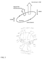
- FIG. 7 explains how the loops are in contact with each other as influenced by the magnetic fields.
- FIG. 8 shows how magnet or a dipole is installed and affected by the magnetic fields.
- FIG. 9 shows how a connecting device is made.
- FIG. 10 describes how the loops spin to achieve memory functions.
- a MOSFET invented in the 1960's, is a “Metal Oxide Semiconductor Field Effect Transistor” (described in FIG. 2 ). It consists of 4 regions: gate, source, drain and substrate. The gate is a conductor. The source and drain are heavily doped conducting semiconductor regions. The gate is separated from the substrate by a layer of insulator, such as silicon dioxide.
- insulator such as silicon dioxide.
- a MOSFET can also be constructed as a “loop”, or in an “ ⁇ ” shape, as shown in FIG. 2 .
- FIG. 4 explains how static magnetic fields can be generated from a metal loop, where electrical current flows. This is the so called “Gauss Law” in Physics. When electrical current flows in a metal loop, magnetic fields are produced.
- the metal loop with electrical current will rotate, influenced by the direction of the external magnetic field. This is explained in FIG. 5 .
- the 3 loops are directly on top of one another.
- the distance between the loops is of atomic scale—only a few nanometers.
- the MOSFET is sandwiched by two electrical current conducting metal loops. There is a specific magnetic field produced by each of the 3 loops. The loops rotate in response to the magnetic fields. The electrical current flowing in the loops become different when the rotation happens and when the loops become in contact with the MOSFET.
- FIG. 6 shows more details of the device. Connecting devices (in small open circles) are specially designed to allow the loops (including the MOSFET) to rotate in the magnetic fields separately. Vertical MOSFETs (to the right) provide additional switching capability to the memory operations.
- FIG. 7 shows how the loops rotate with the magnetic field and can literally be in contact with other loops or the MOSFET.
- the charged areas in each loop and in the MOSFET provide static electrical attractive or repulsive forces, so the loops and the MOSFET can be either in contact with one another or totally be separated, depending on the magnetic fields.
- a dipole, or a magnet can be placed in the magnetic fields to provide memory functions. This is illustrated in FIG. 8 .
- FIG. 9 shows how connecting devices are specially designed to allow rotation movements of each loop and the MOSFET.
- FIG. 10 describes a multiple-loop device where the loops may spin clockwise or counter clockwise in response to magnetic or electrical fields.
- the spin angle can affect the electrical functioning of the MOFET for memory operations.
Landscapes
- Engineering & Computer Science (AREA)
- Chemical & Material Sciences (AREA)
- Nanotechnology (AREA)
- Physics & Mathematics (AREA)
- Mathematical Physics (AREA)
- Theoretical Computer Science (AREA)
- Crystallography & Structural Chemistry (AREA)
- Hall/Mr Elements (AREA)
- Mram Or Spin Memory Techniques (AREA)
- Semiconductor Memories (AREA)
Abstract
Description
Claims (4)
Priority Applications (1)
| Application Number | Priority Date | Filing Date | Title |
|---|---|---|---|
| US13/873,852 US8933519B2 (en) | 2013-04-30 | 2013-04-30 | Magnetic dynamic random access nonvolatile semiconductor memory (MRAM) |
Applications Claiming Priority (1)
| Application Number | Priority Date | Filing Date | Title |
|---|---|---|---|
| US13/873,852 US8933519B2 (en) | 2013-04-30 | 2013-04-30 | Magnetic dynamic random access nonvolatile semiconductor memory (MRAM) |
Publications (2)
| Publication Number | Publication Date |
|---|---|
| US20140319589A1 US20140319589A1 (en) | 2014-10-30 |
| US8933519B2 true US8933519B2 (en) | 2015-01-13 |
Family
ID=51788548
Family Applications (1)
| Application Number | Title | Priority Date | Filing Date |
|---|---|---|---|
| US13/873,852 Active 2033-06-04 US8933519B2 (en) | 2013-04-30 | 2013-04-30 | Magnetic dynamic random access nonvolatile semiconductor memory (MRAM) |
Country Status (1)
| Country | Link |
|---|---|
| US (1) | US8933519B2 (en) |
Citations (1)
| Publication number | Priority date | Publication date | Assignee | Title |
|---|---|---|---|---|
| US7812383B2 (en) * | 2006-09-08 | 2010-10-12 | Kabushiki Kaisha Toshiba | Spin memory and spin FET |
-
2013
- 2013-04-30 US US13/873,852 patent/US8933519B2/en active Active
Patent Citations (1)
| Publication number | Priority date | Publication date | Assignee | Title |
|---|---|---|---|---|
| US7812383B2 (en) * | 2006-09-08 | 2010-10-12 | Kabushiki Kaisha Toshiba | Spin memory and spin FET |
Also Published As
| Publication number | Publication date |
|---|---|
| US20140319589A1 (en) | 2014-10-30 |
Similar Documents
| Publication | Publication Date | Title |
|---|---|---|
| US9599693B2 (en) | Magnetometer with dual purpose reset and calibration coil | |
| US10020039B2 (en) | Three terminal magnetoresistive devices, magnetoresistive random access memory and magnetic recording method | |
| KR101338050B1 (en) | Method of switching out-of-plane magnetic tunnel junction cells | |
| US10897364B2 (en) | Physically unclonable function implemented with spin orbit coupling based magnetic memory | |
| US9882112B2 (en) | Multi-qubit device and quantum computer including the same | |
| US9231194B2 (en) | High stability spintronic memory | |
| US20180190899A1 (en) | Magnetic tunnel junction device with spin-filter structure | |
| EP3053197B1 (en) | Spintronic logic element | |
| KR20180136556A (en) | Magnetic tunnel junction | |
| US20130299880A1 (en) | Spin Transistors Employing a Piezoelectric Layer and Related Memory, Memory Systems, and Methods | |
| EP3486668A1 (en) | Three-axis magnetic sensor | |
| US20160109537A1 (en) | Magneto resistive device | |
| CN104269425B (en) | magnetic field sensor | |
| KR102137476B1 (en) | Magnetic element for memory and logic | |
| US8933519B2 (en) | Magnetic dynamic random access nonvolatile semiconductor memory (MRAM) | |
| CN110190181B (en) | Diode based on ferromagnetic skyrmion | |
| US9523747B2 (en) | Magnetoresistive device and method for manufacturing the same | |
| KR101906708B1 (en) | Asymmetric magnetic devices | |
| US9799823B1 (en) | High temperature endurable MTJ stack | |
| CN102376872A (en) | MOS Transistor Based on Hall Effect | |
| KR100852182B1 (en) | Hybrid semiconductor-ferromagnet device with a junction of positive and negative magnetic-field regions | |
| JP2021025805A (en) | Rotation angle detection sensor | |
| WO2018182644A1 (en) | Spintronic memory with low oxygen precipitation | |
| RU2367059C1 (en) | Tunnel device | |
| Mor et al. | Composed planar Hall effect sensors with dual-mode operation |
Legal Events
| Date | Code | Title | Description |
|---|---|---|---|
| STCF | Information on status: patent grant |
Free format text: PATENTED CASE |
|
| FEPP | Fee payment procedure |
Free format text: MAINTENANCE FEE REMINDER MAILED (ORIGINAL EVENT CODE: REM.); ENTITY STATUS OF PATENT OWNER: SMALL ENTITY |
|
| FEPP | Fee payment procedure |
Free format text: SURCHARGE FOR LATE PAYMENT, SMALL ENTITY (ORIGINAL EVENT CODE: M2554); ENTITY STATUS OF PATENT OWNER: SMALL ENTITY |
|
| MAFP | Maintenance fee payment |
Free format text: PAYMENT OF MAINTENANCE FEE, 4TH YR, SMALL ENTITY (ORIGINAL EVENT CODE: M2551); ENTITY STATUS OF PATENT OWNER: SMALL ENTITY Year of fee payment: 4 |
|
| FEPP | Fee payment procedure |
Free format text: MAINTENANCE FEE REMINDER MAILED (ORIGINAL EVENT CODE: REM.); ENTITY STATUS OF PATENT OWNER: SMALL ENTITY |
|
| FEPP | Fee payment procedure |
Free format text: 7.5 YR SURCHARGE - LATE PMT W/IN 6 MO, SMALL ENTITY (ORIGINAL EVENT CODE: M2555); ENTITY STATUS OF PATENT OWNER: SMALL ENTITY |
|
| MAFP | Maintenance fee payment |
Free format text: PAYMENT OF MAINTENANCE FEE, 8TH YR, SMALL ENTITY (ORIGINAL EVENT CODE: M2552); ENTITY STATUS OF PATENT OWNER: SMALL ENTITY Year of fee payment: 8 |
|
| AS | Assignment |
Owner name: NORTHROP GRUMMAN SYSTEMS CORPORATION, VIRGINIA Free format text: ASSIGNMENT OF ASSIGNORS INTEREST;ASSIGNOR:PAN, JAMES NAN HSI;REEL/FRAME:061063/0390 Effective date: 20220831 |