US8933384B2 - Multi-technique imaging system using vertical motion of stage to switch imaging techniques - Google Patents
Multi-technique imaging system using vertical motion of stage to switch imaging techniques Download PDFInfo
- Publication number
- US8933384B2 US8933384B2 US13/430,316 US201213430316A US8933384B2 US 8933384 B2 US8933384 B2 US 8933384B2 US 201213430316 A US201213430316 A US 201213430316A US 8933384 B2 US8933384 B2 US 8933384B2
- Authority
- US
- United States
- Prior art keywords
- light radiation
- specimen
- sensor
- illumination sources
- imaging
- Prior art date
- Legal status (The legal status is an assumption and is not a legal conclusion. Google has not performed a legal analysis and makes no representation as to the accuracy of the status listed.)
- Active, expires
Links
Images


Classifications
-
- G—PHYSICS
- G01—MEASURING; TESTING
- G01N—INVESTIGATING OR ANALYSING MATERIALS BY DETERMINING THEIR CHEMICAL OR PHYSICAL PROPERTIES
- G01N21/00—Investigating or analysing materials by the use of optical means, i.e. using sub-millimetre waves, infrared, visible or ultraviolet light
- G01N21/17—Systems in which incident light is modified in accordance with the properties of the material investigated
- G01N21/55—Specular reflectivity
-
- G—PHYSICS
- G02—OPTICS
- G02B—OPTICAL ELEMENTS, SYSTEMS OR APPARATUS
- G02B21/00—Microscopes
- G02B21/0004—Microscopes specially adapted for specific applications
- G02B21/0008—Microscopes having a simple construction, e.g. portable microscopes
-
- G—PHYSICS
- G02—OPTICS
- G02B—OPTICAL ELEMENTS, SYSTEMS OR APPARATUS
- G02B21/00—Microscopes
- G02B21/18—Arrangements with more than one light path, e.g. for comparing two specimens
-
- G—PHYSICS
- G02—OPTICS
- G02B—OPTICAL ELEMENTS, SYSTEMS OR APPARATUS
- G02B21/00—Microscopes
- G02B21/36—Microscopes arranged for photographic purposes or projection purposes or digital imaging or video purposes including associated control and data processing arrangements
-
- G—PHYSICS
- G01—MEASURING; TESTING
- G01N—INVESTIGATING OR ANALYSING MATERIALS BY DETERMINING THEIR CHEMICAL OR PHYSICAL PROPERTIES
- G01N21/00—Investigating or analysing materials by the use of optical means, i.e. using sub-millimetre waves, infrared, visible or ultraviolet light
- G01N21/17—Systems in which incident light is modified in accordance with the properties of the material investigated
- G01N21/47—Scattering, i.e. diffuse reflection
- G01N21/4788—Diffraction
- G01N2021/479—Speckle
-
- G—PHYSICS
- G01—MEASURING; TESTING
- G01N—INVESTIGATING OR ANALYSING MATERIALS BY DETERMINING THEIR CHEMICAL OR PHYSICAL PROPERTIES
- G01N21/00—Investigating or analysing materials by the use of optical means, i.e. using sub-millimetre waves, infrared, visible or ultraviolet light
- G01N21/17—Systems in which incident light is modified in accordance with the properties of the material investigated
- G01N21/55—Specular reflectivity
- G01N2021/558—Measuring reflectivity and transmission
-
- G—PHYSICS
- G01—MEASURING; TESTING
- G01N—INVESTIGATING OR ANALYSING MATERIALS BY DETERMINING THEIR CHEMICAL OR PHYSICAL PROPERTIES
- G01N21/00—Investigating or analysing materials by the use of optical means, i.e. using sub-millimetre waves, infrared, visible or ultraviolet light
- G01N21/17—Systems in which incident light is modified in accordance with the properties of the material investigated
- G01N21/47—Scattering, i.e. diffuse reflection
- G01N21/4788—Diffraction
-
- G—PHYSICS
- G01—MEASURING; TESTING
- G01N—INVESTIGATING OR ANALYSING MATERIALS BY DETERMINING THEIR CHEMICAL OR PHYSICAL PROPERTIES
- G01N21/00—Investigating or analysing materials by the use of optical means, i.e. using sub-millimetre waves, infrared, visible or ultraviolet light
- G01N21/17—Systems in which incident light is modified in accordance with the properties of the material investigated
- G01N21/55—Specular reflectivity
- G01N21/552—Attenuated total reflection
- G01N21/553—Attenuated total reflection and using surface plasmons
- G01N21/554—Attenuated total reflection and using surface plasmons detecting the surface plasmon resonance of nanostructured metals, e.g. localised surface plasmon resonance
-
- G—PHYSICS
- G01—MEASURING; TESTING
- G01N—INVESTIGATING OR ANALYSING MATERIALS BY DETERMINING THEIR CHEMICAL OR PHYSICAL PROPERTIES
- G01N21/00—Investigating or analysing materials by the use of optical means, i.e. using sub-millimetre waves, infrared, visible or ultraviolet light
- G01N21/62—Systems in which the material investigated is excited whereby it emits light or causes a change in wavelength of the incident light
- G01N21/63—Systems in which the material investigated is excited whereby it emits light or causes a change in wavelength of the incident light optically excited
- G01N21/64—Fluorescence; Phosphorescence
- G01N21/645—Specially adapted constructive features of fluorimeters
- G01N21/6456—Spatial resolved fluorescence measurements; Imaging
-
- G—PHYSICS
- G01—MEASURING; TESTING
- G01N—INVESTIGATING OR ANALYSING MATERIALS BY DETERMINING THEIR CHEMICAL OR PHYSICAL PROPERTIES
- G01N21/00—Investigating or analysing materials by the use of optical means, i.e. using sub-millimetre waves, infrared, visible or ultraviolet light
- G01N21/62—Systems in which the material investigated is excited whereby it emits light or causes a change in wavelength of the incident light
- G01N21/63—Systems in which the material investigated is excited whereby it emits light or causes a change in wavelength of the incident light optically excited
- G01N21/65—Raman scattering
-
- G—PHYSICS
- G01—MEASURING; TESTING
- G01N—INVESTIGATING OR ANALYSING MATERIALS BY DETERMINING THEIR CHEMICAL OR PHYSICAL PROPERTIES
- G01N2201/00—Features of devices classified in G01N21/00
- G01N2201/02—Mechanical
- G01N2201/022—Casings
- G01N2201/0221—Portable; cableless; compact; hand-held
-
- G—PHYSICS
- G01—MEASURING; TESTING
- G01N—INVESTIGATING OR ANALYSING MATERIALS BY DETERMINING THEIR CHEMICAL OR PHYSICAL PROPERTIES
- G01N2201/00—Features of devices classified in G01N21/00
- G01N2201/06—Illumination; Optics
- G01N2201/069—Supply of sources
- G01N2201/0693—Battery powered circuitry
Definitions
- Imaging and diffraction-based measurements are widely-used in nearly all areas of research.
- most current imaging systems are designed for specific table-top experiments, occupy large spaces, and require trained personnel for operation.
- most imaging systems today are designed to handle only one technique of microscopy, e.g., bright field imaging.
- a user today In order to perform more than one optical analysis technique (i.e., illumination and measurement by multiple sources, such as, for example, white light illumination for bright field imaging and laser illumination for diffractometry), a user today must typically transport the user's sample from one imaging system to another imaging system.
- the sample must be re-positioned and re-aligned. Such positioning can be cumbersome and lead to inaccuracies.
- imaging equipment in use today is typically large and not portable.
- a compact, portable system that can perform multi-technique imaging including bright field imaging and diffractometric analysis of sample chip surfaces can be extremely useful both in lab usage and point-of-care applications. Therefore, there exists a need for a system for performing optical imaging and diffraction measurements, analyze the associated data, store the raw data and the analyzed data, and display and communicate the analyzed data, all in one package that contains light-weight components and occupies a relatively small space, without the need of transporting the analyzed specimen from one experimental setup to another.
- a system and method for performing multi-technique imaging includes a surface for supporting a specimen and at least two illumination sources for producing light radiation.
- the system also includes a plurality of reflective and refractive devices configured to direct at least part of the light radiation from each of the at least two illumination sources to the surface such that at least part of the light radiation from each of the at least two illumination sources illuminate substantially the same area on the surface (i.e. illuminating the same area on the specimen).
- the system further includes a sensor configured to receive light radiation from the at least two illumination sources reflected by the specimen and/or that pass by the specimen.
- the system additionally includes a power source configured to power the at least two illumination sources and the sensor.
- a method for performing multi-technique imaging includes the step of arranging a plurality of reflective and/or refractive devices to direct at least part of light radiation from each of at least two illumination sources in the direction of a surface supporting a specimen such that at least part of the light radiation from each of the at least two illumination sources illuminate substantially the same area on the surface and pass through a shared reflective and/or refractive device.
- the method also includes the step of activating the at least two illumination sources to produce light radiation.
- the method further includes collecting the light radiation from the at least two illumination sources reflected by the specimen.
- FIG. 1 depicts a schematic view of one embodiment of the system for performing multi-technique imaging according to the present disclosure.
- FIG. 2 a depicts a perspective view of one embodiment of a portable multi-technique imaging system (PMMIS) including a screen for displaying data, according to the present disclosure.
- PMMIS portable multi-technique imaging system
- FIG. 2 b depicts a side view of one embodiment of a PMMIS, showing the optical, electronic and manipulation stage components according to the present disclosure.
- FIG. 2 c depicts a top view of one embodiment of a PMMIS, showing the microscopic image of a specimen with receptor sites on the screen, according to the present disclosure.
- FIG. 2 d depicts a top view of one embodiment of a PMMIS, revealing the internal optical components, according to the present disclosure.
- FIGS. 2 e - 2 g depict an illustration of one embodiment of a manipulator according to the present disclosure.
- FIG. 3 depicts a view of a side of a PMMIS, revealing electronic circuits for analysis, control, and communication according to one embodiment of the present disclosure.
- FIG. 4 a depicts a schematic view of an exemplary embodiment of a PMMIS according to the present disclosure with bright field and laser illumination of a target chip.
- FIG. 4 b depicts a schematic of an exemplary embodiment of a PMMIS according to the present disclosure showing bright field imaging and diffractometry performed on the same stage, using the same objective lens, and the same image plane of the PMMIS and resulting images on the image plane.
- FIGS. 5 a - 5 b depict bright field microscopic images of a sample target chip with 1) ideal (microfabricated) diffraction grating ( FIGS. 5 b ), and 2) with the receptor sites having particles bound thereto ( FIG. 5 a ).
- FIGS. 6 a - 6 b depict views from sample target chips with diffractometric analysis with 1) laser illumination of diffraction grating of FIG. 5 b ( FIGS. 6 b ), and 2) with preprinted receptor sites with particles bound thereto ( FIG. 6 a ).
- FIG. 7 depicts a schematic view of an exemplary system according to at least one embodiment of the present disclosure utilizing a bright field apparatus and a laser speckle apparatus for illumination of a target chip.
- FIG. 8 shows an exemplary system according to at least one embodiment of the present disclosure utilizing a confocal laser apparatus and a bright field imaging apparatus.
- FIG. 9 shows an exemplary system of at least one embodiment of the present disclosure utilizing a Raman spectrometer apparatus.
- FIG. 10 shows a schematic layout of one embodiment of the control systems and electronics according to the present disclosure.
- FIG. 11 shows a flowchart of a method of performing multi-technique imaging according to at least one embodiment of the present disclosure.
- FIG. 1 shows a diagram of an exemplary system 100 of at least one embodiment of the present disclosure.
- the system 100 includes a stage 105 for supporting and manipulating a specimen, two or more illumination sources 110 , and two or more reflective and/or refractive devices 120 that are arranged to direct at least part of the light radiation from the two or more illumination sources 110 to the stage 105 ,
- the illumination. sources 110 may be various devices that produce radiation including, light, such as, for example, a device for producing :laser light, a device for producing white light, and a device for producing colored light (i.e., non-white).
- a light can be configured to provide light in any part of the electromagnetic spectrum, including but not limited to visible light of different colors, including white light, infrared, X-ray, and other type of light known to a person having ordinary skill in the art.
- Light can be of a highly propagating nature or of a collimated nature, e.g., a laser.
- the dashed lines in FIG. 1 show pathways of light radiation from the illumination sources 110 .
- the system 100 also includes a sensor 130 for receiving light radiation from the at least two illumination sources 110 .
- the sensor 130 may receive light radiation that is reflected by the specimen and/or when the light radiation passes by the specimen.
- the system 100 may be arranged such that the sensor is on the same side of the stage as the specimen (thereby receiving the reflected light radiation from the specimen) or such that the sensor is on the opposite side of the stage as the specimen (thereby receiving the light radiation after it passes by the specimen), While FIG. 1 only shows one sensor 130 , the system 100 may include multiple sensors 130 for collecting light radiation. While not shown in FIG.
- the system 100 also includes a power source for powering the illumination devices 110 and sensor 130 .
- a power source for powering the illumination devices 110 and sensor 130 .
- the arrangement of the system 100 allows a user to perform multiple imaging analysis techniques on a specimen without having to transport the specimen to and realign the specimen on multiple types of imaging equipment.
- FIGS. 2 a - 2 d , 3 , and 4 show an example of the system 100 , namely a portable multi-technique imaging system (PMMIS) 100 a suitable for point of care applications.
- PMMIS portable multi-technique imaging system
- FIGS. 2 a - 2 d , 3 , and 4 show an example of the system 100 , namely a portable multi-technique imaging system (PMMIS) 100 a suitable for point of care applications.
- PMMIS portable multi-technique imaging system
- the system of the present disclosure may be placed on a lab bench, or easily carried by a person to another location where without limitation the system of the present disclosure is powered up by an internal power interface, e.g., a battery, the specimen is inserted into the system, the specimen is analyzed, the analyzed data is saved on to a memory device, e.g., a hard drive, and the analyzed data is communicated to another device using a wireless communication interface and over a network, e.g., the internet.
- FIG. 2 a shows a perspective view of the PMMIS 100 a .
- the PMMIS 100 a can be used with test chips with receptor sites and functionalized magnetic beads, which trap and localize molecular structures that are sized in the micrometer to nanometer range.
- the PMMIS 100 a depicted in FIG. 2 a includes a screen or display 102 a , a control knob 104 a , control buttons 106 a , manipulation stage 105 a , communication and control circuits 108 a , which includes an on-board computer, that connect and process information between the display 102 a , control knob 104 a , control buttons 106 a , manipulation stage 105 n , sensor 130 a (not shown) to each other and other parts of the PMMIS 100 a .
- the screen 102 a is configured to display information and analysis results to the user regarding the light radiation received by the sensor 130 a (discussed below).
- the screen 102 a may be various types of devices known in the art designed to display electronic information.
- the screen 102 a may be a touch screen configured to present menus and read inputs from a user touching the screen 102 a .
- the control knob 104 a and the control buttons 106 n may be configured to control various operations of the PMMIS 100 a , including light intensity, activation of light sources, and powering the system on and off.
- the PMMIS 100 a may include wireless and/or wired communication provisions for communicating with external sources (e.g., a personal computer, an external display unit, a distant receiver and a printer).
- FIGS. 2 b and 2 c the PMMIS 100 a of FIG. 2 a is depicted from side and top view perspectives.
- a manipulator 107 a that is configured to adjust the position of a specimen.
- the manipulator 107 a may be any type of device configured to adjust the position of the specimen, such as, for example, a micro-manipulator.
- the manipulator 107 a can be manually controlled or controlled electronically by use of servo and stepper motors, known to a person of ordinary skill in the art.
- the vertical motion of the stage of the manipulator 107 a may be controlled manually by a micrometer.
- the x and y (horizontal) motions of the stage may be controlled by two separate stepper motors with leadscrew interfaces.
- the motors may be controlled by the on-board computer.
- a user can touch a button or portion of the screen and the stage will move right or left.
- a user can program the on-board computer to move the stage in a pre-determined state (e.g., to scan at least a part of the surface).
- FIG. 2 b Shown in FIG. 2 b is a manipulator 107 a that is integrated in the PMMIS 100 a .
- the communication and control circuits 108 a may be configured to automatically control the manipulator 107 a under control of software.
- FIGS. 2 e - 2 f show an illustration of one embodiment of a manipulator 107 a according to the present disclosure.
- the manipulator 107 a includes a first plate FP for supporting a specimen and a second plate SP for supporting the first plate FP and a first linear pack FLP that allows the first plate FP to slide relative to the second plate in the X direction as defined in FIG. 2 e .
- the manipulator 107 a also includes a third plate TP for supporting the second plate SP and one or more second linear packs SLP that allow the second plate SP to slide relative to the third plate TP in the Y direction as defined in FIG. 2 e .
- FIG. 2 g shows an example of a first linear pack FLP and second linear pack SLP.
- the manipulator 107 a also includes a shaft S that is integrated with the third plate TP such that all of the plates FP, SP, TP can be moved in the Z direction (as defined in FIG. 2 e ) manually or automatically through the use of various devices, such as, for example, a micrometer.
- 2 e and 2 f also show calibration devices CD that allow the various plates FP, SP, TP to be moved along the X, Y, and Z directions.
- manipulator 107 a may also include a corresponding stepper motor with lead screw calibration device that allows either a computer or user to electrically manipulate the position of the specimen in any of the X or Y directions as needed.
- FIG. 2 c Shown in FIG. 2 c is the top view of PMMIS 100 a showing a real-time microscopic image of a specimen that has microscopic receptor sites (RS) with magnetic micro and nanoparticles immobilized in a manner mediated by a biomolecular reaction.
- the on-board computer of PMMIS 100 a can be programmed to perform multiple types of image analysis including but not limited to identifying and counting entities and analyzing their properties.
- FIG. 2 d the PMMIS of FIG. 2 a is depicted with the screen lifted to reveal internal components of the PMMIS.
- FIG. 2 d shows two illumination sources 110 a (namely, a bright field (white light) source and a laser source), a sensor (namely, a charge coupled device (CCD)) 130 a , a wireless antenna 190 a , and a motion controller 192 a (shown in FIG. 2 b ) for the manipulator 107 a .
- the sensor can be various devices for collecting light radiation, such as, for example, the CCD model DCU223C from Thorlabs.
- the sensor may be various other CMOS devices or digital imaging sensors instead of a CCD.
- the sensor may be a photodiode digital image sensor.
- the motion controller 192 a may be part of the communication and control circuits 108 a , more clearly depicted in FIGS. 2 b and 3 .
- the PMMIS 100 a depicted in FIGS. 2 a - d and 3 includes bright field and laser diffractometry capabilities
- the PMMIS 100 a may have additional or alternative capabilities by way of other microscopic techniques. Such other techniques as well as bright field and diffractometry techniques are discussed below.
- FIG. 4 a a schematic of the PMMIS 100 a of FIGS. 2 a - 2 d and 3 is depicted.
- a laser diode 110 ai e.g., a 635 nm laser source
- the laser light from the laser diode 110 ai is polarized as it passes through a polarizer 109 a and reflected (and redirected) by striking a reflection surface M 2 .
- the laser light passes through reflective device BS 2 and lens L 1 and is redirected by reflective device BS 1 .
- a white light 110 aii e.g., a 3500K light source, bright field source
- a bright field e.g. white
- the white light may be a single LED combined with a color wheel or a collection of LEDs with different colors to generate illumination with different wavelengths. This arrangement can be used for white light imaging, diffractometry, multi-wavelength bright field imaging as well as fluorescence microscopy, by introducing a movable wavelength filter before the image sensor 130 a.
- the bright field light is condensed through a condenser 108 a and is redirected by reflective device BS 2 .
- the bright field light then passes through lens L 1 and is redirected by reflective device BS 1 .
- the bright field light then is redirected by reflective device M 1 so that it passes through objective lens 150 a and strikes the stage 105 a .
- the PMMIS 100 a is able to provide epi-illumination for bright field imaging and diffraction measurement of specimens.
- the reflection/diffraction from the specimen passes through the objective lens 150 a and is captured by the image sensor (e,g.
- the reflective and refractive devices 120 of a system 100 of the present disclosure may be any type of device configured to reflect or refract light radiation known to one skilled in the art, such as, for example, a mirror or a refractive component such as a lens.
- the reflective and refractive devices can include, but are not limited to, mirrors, dichroic mirrors, and converging and diverging lenses.
- the reflective and refractive devices may be selected and positioned for particular results.
- the reflective and refractive devices may be arranged such that the incident light is focused at the back focal plane of an objective lens, so as to generate a plane wave front to impinge on the specimen that is the subject of a diffraction measurement.
- the diffraction pattern generated by the specimen e.g. a linear grating
- the specimen can be moved further away (beyond the front focal plane or FFP of the objective lens) for bright field imaging.
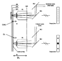
- FIG. 4 b shows an example of the specimen being moved closer to the objective lens (OL) for diffractometry and away from it for bright field imaging.
- the distance DWL between the specimen and the closest part of the objective lens for bright field imaging is greater than the distance DL between the specimen and the closest edge of the objective lens for diffractometry.
- Such a scheme would also allow “co-incident” imaging and diffractometry of the same area on the specimen using a single objective lens and a single image sensor (such as a CCD).
- FIG. 7 shows an exemplary system 100 b utilizing a bright field apparatus 110 bi and a laser speckle apparatus 110 bii for illumination of a stage 105 b in an arrangement the same as to the system 105 a in FIG. 4A but without lens L 1 .
- FIG. 7 shows an exemplary system 100 b utilizing a bright field apparatus 110 bi and a laser speckle apparatus 110 bii for illumination of a stage 105 b in an arrangement the same as to the system 105 a in FIG. 4A but without lens L 1 .
- FIG. 8 shows a schematic of an exemplary system 100 r utilizing a confocal laser apparatus and a bright field imaging apparatus, which includes one or more disks with spiral holes DS and a beam expander BE in the path of the light source 110 ri.
- FIG. 9 shows a schematic of an exemplary system 100 z utilizing a Raman spectrometer apparatus including a filter F, grating G, and second sensor 130 zi for receiving light radiation from a grating G.
- FIGS. 5 a - 5 b show examples of bright field imaging results from a test chip.
- FIGS. 5 a - 5 b show light radiation received by the sensor 130 a and displayed on screen 102 a of the PMMIS 100 a .
- FIG. 5 a shows receptor sites RS that are preprinted on the test chip using a micro-stamping process. After the micro-stamping process, anti-body coupled magnetic beads that have attracted certain target entities (such as proteins, peptides, small molecules, DNA, RNA, bacteria, cells and viruses) can be implemented on the test chip for a periodic arrangement.
- target entities such as proteins, peptides, small molecules, DNA, RNA, bacteria, cells and viruses
- the magnetic beads selected for use are detectable through bright field detection and/or through laser diffractometry or other technique and can be analyzed and counted by an optional on-board counting algorithm programmed into an on-board computer of the device and studied. Strips of binder material may also be used on the test chip to selectively bind certain proteins.
- FIG. 5 a depicts the particles in the receptor sites detected through bright field imaging. A broad range of biological entities may be detected using the system 100 of the present disclosure from small molecules to biomolecules (including proteins, DNA, and RNA) to bacteria, viruses, and cells by using the appropriate receptor combinations for the chip and the beads.
- FIG. 5 b shows the micrograph of an example of a microfabricated diffraction grating structure.
- optical modes produced by laser diffractometry are depicted using laser diffractometry.
- a sample with a specific pattern is illuminated with a coherent light source (e.g., a laser)
- the light beams that reflect from the alternating lines with different phases e.g, particle baring lines and empty lines in between; or the lines in a microfabricated grating that have different heights or refractive indices
- the intensities of the modes depend on the phase difference between the lines.
- the detection of mode intensities can reveal information about, height, refractive index of fabricated grating structure and/or the medium it is in; as well as quantity and various geometrical and optical properties of the particles that constitute the gratings.
- the diffraction pattern depends on the pattern of the grating itself. As shown in FIG. 5 b , the microfabricated grating MG is represented as vertical columns. In the case of FIGS. 5 a and 5 b , since the periodicity of the samples are one dimensional, the resulting diffraction pattern is also one dimensional (all modes are in one line). It should be noted that the system 100 according to the present disclosure can capture and analyze diffraction patterns produced by other kinds of patterns having multiple dimensions.
- FIG. 6 a depicts the diffraction modes from the receptor sites having particles bound thereto. Depicted are the zero mode ZM and the first mode FM symmetric about the zero mode ZM. In FIG. 6 b , these modes are visible even though they are dimmer as compared to the modes depicted in FIG. 6 a.
- FIGS. 5 a - 5 b and 6 a - 6 b show the results of radiation collection for one technique
- the system may be configured to collect radiation and display corresponding information regarding multiple techniques. For instance, while images from each source of light can be sequentially formed on the sensor, the system according to the present disclosure may be configured to simultaneously form the images on the sensor to provide an overlay of the images. This capability is particularly useful when there is a high temporal activity on the specimen, and images from various techniques each can provide data about the specimen, simultaneously and as a function of time.
- the system 100 provides imaging and detection capabilities in a co-incident, co-located, and optionally simultaneous manner for a variety of applications.
- a user can switch between one imaging technique (e.g., bright field illumination and capture) to another (e.g., laser diffractometry) without having to move the specimen horizontally out of position which enables diffractometric and bright field imaging of the same area on the specimen.
- the specimen may be moved vertically closer to or away from an objective lens for focusing or divergence of a reflected pattern as needed (without losing the microscopic field of view on the specimen.)
- One may also use multiple light sources and imaging techniques simultaneously including, but not limited to, bright field and laser speckle imaging.
- a combination or all of the following analysis techniques can be performed by the system: bright field imaging, dark-field imaging and surface plasmon resonance (by introducing illumination at an angle via a fiberoptic cable, with an occulting disk for dark field imaging), video imaging, localized surface plasmon resonance, interferometry, diffractometry (including binding of biological entities such as cells, viruses and biomolecules via affinity interactions with and without magnetic and nonmagnetic beads and spheres where such binding is random or guided by a pre-defined functional pattern), Michelson interferometry, speckle imaging, fluorescence imaging, spectroscopy, spectrophotometry, Raman spectroscopy, and confocal microscopy, among others.
- Each of the techniques used in the system 100 can reveal specific information about the specimen including, but not limited to, refractive index, molecular or material composition, physical and chemical properties, dimensions, phase, and color.
- the system 100 according to the present disclosure can obtain and provide information to the user from any combination of these techniques.
- the analysis of a specific microscopic area on a specimen with multiple imaging techniques can be accomplished without the need for removing and re-aligning the specimen.
- the system 100 of the present disclosure allows executing various interrogation and detection techniques sequentially or simultaneously, at the control of the user, or as controlled by an on-board computer. For example, a user may switch between one light source to another light source by pressing a button 106 a or a button on a touch screen 102 a . Such immediate control can allow the user to switch techniques quickly in order to observe specimen events as they are happening.
- the quantity, activity, and properties (including, but not limited to, dimensions, composition, refractive index, and patterns) of biological entities such as cells, viruses, biomolecules, small molecules, bacteria and spores can be detected and analyzed in an efficient and controlled manner.
- the information can be location-tagged by introducing a GPS-enabled chip, shared wirelessly by introducing a wireless card or via a USB interface.
- the system 100 according to the present disclosure may be particularly beneficial for imaging or detecting activities which may require multiple techniques (e.g., bright field and laser diffractometry). For example, the time period during which cell cycle activities or bacteria colonization occur may be short. Conventional imaging methods and apparatuses are not effective with regard to such activities and colonization because it takes too long to move and align the specimen from one system to another system and such motion and alignment introduces errors. By contrast, the system 100 of the present disclosure can effectively be used to provide multi-technique imaging in a short period of time.
- multiple techniques e.g., bright field and laser diffractometry
- the system 100 may be operated in a simultaneous mode (i.e., light sources each providing light radiation at the same time) or in a switching sequence mode where the system 100 can be switched from one technique to another (e.g., turn on the laser and capture a diffraction image for a fraction of a second, turn laser off, turn white light on and capture image for a fraction of a second).
- a switching sequence may be controlled by the user or can be controlled by an on-board computer. Since the interrogation of the specimen is co-incident, images from the same location on the specimen can be generated using multiple techniques.
- the communication and control circuits 108 a may include a variety of devices for carrying out the control, analysis, process, and other functions of the system of the present disclosure. Such functions include data acquisition, processing, display, user interface, scanning stage control, wired and wireless communication, peripheral control and power management.
- a schematic layout of the electronics is shown in FIG. 10 .
- the power supply of the system may be powered by a battery and/or another power source (e.g., wall power), which then feeds the other components of the system, including the communication and control circuits 108 a (e.g., embedded computer), screen, wireless components, illumination sources, sensor, and the like.
- the communication and control circuits 108 a may include a low-power embedded on-board computer (e.g.
- igologic i2820 running an operating system (e.g. Windows XP) which provides graphical user interface (GUI) based control, data acquisition and processing.
- GUI graphical user interface
- Data from an image sensor e.g. DCU223C, Thorlabs, NJ, USA
- a high resolution LCD display and a sunlight readable touchscreen e.g. Panjit, AZ, USA
- Various mechanisms may be provided for connection to external peripherals for data sharing (e.g. a USB connector) and wireless communication (e.g. a 802.11b/g embedded WiFi module, VNT6656, VIA, Taiwan or a GSM module) or cabled connection (e.g. local area network connection).
- the system of the present disclosure may be powered in a variety of ways, such as by a high wattage ATX (Advanced Technology Extended) power supply (e.g. 120 W, PicoPSU, e-ITX, CA, USA) through a custom designed printed circuit board with compatible connectors as well as circuits and components for power on/off operation, regulation, relays, LED driver (e.g. 7021 BuckPlus, LEDdynamics, USA) as well as to power any additional component.
- An analog output of 0-1 V from the DAQ (Data Acquisition Board) may be included to control the power output from an LED while a potentiometer with a knob mounted on the display deck ( 104 a ) can be used for LED dimming control.
- the stage motor controller e.g. TMCM-343, Trinamic Motion Control GmbH, Germany
- TMCM-343 Trinamic Motion Control GmbH, Germany
- FIG. 11 shows a flowchart of a method for performing multi-technique imaging 1000 .
- the method 1000 includes the step 1001 of arranging a plurality of reflective devices to direct at least part of light radiation from each of at least two illumination sources in the direction of a surface supporting a specimen such that the at least part of the light radiation from each of the at least two illumination sources are substantially coincident on the specimen.
- the method 1000 also includes the step 1003 of activating the at least two illumination sources to produce light radiation.
- the method 1000 further includes the step 1005 of collecting the light radiation from the at least two illumination sources reflected or transmitted by the specimen.
- the method 1000 optionally includes the step 1007 of analyzing at least a portion of the collected light radiation and the step 1008 of displaying at least a portion of the collected light radiation and/or the results of the analysis of the collected light radiation.
Landscapes
- Physics & Mathematics (AREA)
- Chemical & Material Sciences (AREA)
- Analytical Chemistry (AREA)
- General Physics & Mathematics (AREA)
- Optics & Photonics (AREA)
- Life Sciences & Earth Sciences (AREA)
- Health & Medical Sciences (AREA)
- Biochemistry (AREA)
- General Health & Medical Sciences (AREA)
- Immunology (AREA)
- Pathology (AREA)
- Engineering & Computer Science (AREA)
- Multimedia (AREA)
- Investigating Or Analysing Materials By Optical Means (AREA)
- Microscoopes, Condenser (AREA)
Abstract
Description
Claims (20)
Priority Applications (1)
| Application Number | Priority Date | Filing Date | Title |
|---|---|---|---|
| US13/430,316 US8933384B2 (en) | 2011-03-25 | 2012-03-26 | Multi-technique imaging system using vertical motion of stage to switch imaging techniques |
Applications Claiming Priority (2)
| Application Number | Priority Date | Filing Date | Title |
|---|---|---|---|
| US201161467815P | 2011-03-25 | 2011-03-25 | |
| US13/430,316 US8933384B2 (en) | 2011-03-25 | 2012-03-26 | Multi-technique imaging system using vertical motion of stage to switch imaging techniques |
Publications (2)
| Publication Number | Publication Date |
|---|---|
| US20120241596A1 US20120241596A1 (en) | 2012-09-27 |
| US8933384B2 true US8933384B2 (en) | 2015-01-13 |
Family
ID=46876523
Family Applications (1)
| Application Number | Title | Priority Date | Filing Date |
|---|---|---|---|
| US13/430,316 Active 2032-11-20 US8933384B2 (en) | 2011-03-25 | 2012-03-26 | Multi-technique imaging system using vertical motion of stage to switch imaging techniques |
Country Status (1)
| Country | Link |
|---|---|
| US (1) | US8933384B2 (en) |
Families Citing this family (3)
| Publication number | Priority date | Publication date | Assignee | Title |
|---|---|---|---|---|
| US9874736B2 (en) * | 2013-04-29 | 2018-01-23 | The Regents Of The University Of California | Apparatus and method for an inclined single plane imaging microscope box (iSPIM box) |
| JP6588055B2 (en) * | 2017-06-09 | 2019-10-09 | 株式会社シバサキ | Bacteria detection device |
| JP2023539776A (en) * | 2020-09-04 | 2023-09-19 | アイ―アブラ リミテッド | Apparatus and method for analysis, sample containers, caps of sample containers |
Citations (2)
| Publication number | Priority date | Publication date | Assignee | Title |
|---|---|---|---|---|
| US6635011B1 (en) * | 2000-01-14 | 2003-10-21 | Pentax Corporation | Electronic endoscope system |
| US20070120069A1 (en) * | 2005-11-30 | 2007-05-31 | Olympus Corporation | Laser-scanning microscope system |
-
2012
- 2012-03-26 US US13/430,316 patent/US8933384B2/en active Active
Patent Citations (2)
| Publication number | Priority date | Publication date | Assignee | Title |
|---|---|---|---|---|
| US6635011B1 (en) * | 2000-01-14 | 2003-10-21 | Pentax Corporation | Electronic endoscope system |
| US20070120069A1 (en) * | 2005-11-30 | 2007-05-31 | Olympus Corporation | Laser-scanning microscope system |
Also Published As
| Publication number | Publication date |
|---|---|
| US20120241596A1 (en) | 2012-09-27 |
Similar Documents
| Publication | Publication Date | Title |
|---|---|---|
| JP6513802B2 (en) | Laser light coupling for nanoparticle detection | |
| US9683938B2 (en) | Fluorescent imaging using a flatbed scanner | |
| US10578851B2 (en) | Automated hardware and software for mobile microscopy | |
| US20130260382A1 (en) | Systems and methods for utilizing microscopy | |
| EP2930496B1 (en) | Raman micro-spectrometry system and method for analyzing microscopic objects in a fluidic sample | |
| US20090045351A1 (en) | Sensor system with surface-plasmon-polariton (spp) enhanced selective fluorescence excitation and method | |
| US8633432B2 (en) | Reflective focusing and transmissive projection device | |
| JP2010507828A (en) | System for imaging an object | |
| Ghosh et al. | A compact photonic resonator absorption microscope for point of care digital resolution nucleic acid molecular diagnostics | |
| KR20220148163A (en) | Digital Microfluidics Systems, Cartridges and Methods Including Integrated Refractive Index Sensing | |
| US8933384B2 (en) | Multi-technique imaging system using vertical motion of stage to switch imaging techniques | |
| CA3136484A1 (en) | Assay apparatuses, methods and reagents | |
| JP2025130717A (en) | Methods and related systems for localization and spectral imaging of microparticles | |
| JP2003524180A (en) | Fluorescence detection device and its detection method | |
| JP2013545989A (en) | Systems and methods for imaging by complex techniques used for chemical, biological or biochemical analysis of samples | |
| WO2016020514A1 (en) | Ultra-compact microscope with autofocusing | |
| JPH10293133A (en) | Scanning proximity field optical microscope | |
| Liu et al. | Underwater Raman microscopy—a novel in situ tool for deep-sea microscale target studies | |
| AU2002228571A1 (en) | Test method | |
| KR20120125745A (en) | Bio-chip detector | |
| CN101218483B (en) | Three-dimensional position observation method and device | |
| CN109668869A (en) | A kind of hand-held reflection Confocal laser-scanning microscopy detection device | |
| EP4062150B1 (en) | Trace microanalysis microscope systems and methods | |
| CN117070336A (en) | Fluorescence detection system for digital polymerase chain reaction | |
| US20130134293A1 (en) | Optical examinations with controlled input light |
Legal Events
| Date | Code | Title | Description |
|---|---|---|---|
| AS | Assignment |
Owner name: PURDUE RESEARCH FOUNDATION, INDIANA Free format text: ASSIGNMENT OF ASSIGNORS INTEREST;ASSIGNORS:SAVRAN, CAGRI A.;ARIF, KHALID M.;SIGNING DATES FROM 20120824 TO 20121128;REEL/FRAME:029382/0057 |
|
| AS | Assignment |
Owner name: NATIONAL INSTITUTES OF HEALTH (NIH), U.S. DEPT. OF Free format text: CONFIRMATORY LICENSE;ASSIGNOR:PURDUE UNIVERSITY;REEL/FRAME:029777/0373 Effective date: 20130206 |
|
| STCF | Information on status: patent grant |
Free format text: PATENTED CASE |
|
| FEPP | Fee payment procedure |
Free format text: SURCHARGE FOR LATE PAYMENT, SMALL ENTITY (ORIGINAL EVENT CODE: M2554); ENTITY STATUS OF PATENT OWNER: SMALL ENTITY |
|
| MAFP | Maintenance fee payment |
Free format text: PAYMENT OF MAINTENANCE FEE, 4TH YR, SMALL ENTITY (ORIGINAL EVENT CODE: M2551); ENTITY STATUS OF PATENT OWNER: SMALL ENTITY Year of fee payment: 4 |
|
| FEPP | Fee payment procedure |
Free format text: 7.5 YR SURCHARGE - LATE PMT W/IN 6 MO, SMALL ENTITY (ORIGINAL EVENT CODE: M2555); ENTITY STATUS OF PATENT OWNER: SMALL ENTITY |
|
| MAFP | Maintenance fee payment |
Free format text: PAYMENT OF MAINTENANCE FEE, 8TH YR, SMALL ENTITY (ORIGINAL EVENT CODE: M2552); ENTITY STATUS OF PATENT OWNER: SMALL ENTITY Year of fee payment: 8 |