US8916862B2 - Organic EL panel, display device using same, and method for producing organic EL panel - Google Patents
Organic EL panel, display device using same, and method for producing organic EL panel Download PDFInfo
- Publication number
- US8916862B2 US8916862B2 US13/819,059 US201013819059A US8916862B2 US 8916862 B2 US8916862 B2 US 8916862B2 US 201013819059 A US201013819059 A US 201013819059A US 8916862 B2 US8916862 B2 US 8916862B2
- Authority
- US
- United States
- Prior art keywords
- colors
- film thickness
- light
- layer
- layers
- Prior art date
- Legal status (The legal status is an assumption and is not a legal conclusion. Google has not performed a legal analysis and makes no representation as to the accuracy of the status listed.)
- Active
Links
Images


Classifications
-
- H01L51/5203—
-
- H—ELECTRICITY
- H05—ELECTRIC TECHNIQUES NOT OTHERWISE PROVIDED FOR
- H05B—ELECTRIC HEATING; ELECTRIC LIGHT SOURCES NOT OTHERWISE PROVIDED FOR; CIRCUIT ARRANGEMENTS FOR ELECTRIC LIGHT SOURCES, IN GENERAL
- H05B33/00—Electroluminescent light sources
- H05B33/12—Light sources with substantially two-dimensional [2D] radiating surfaces
- H05B33/14—Light sources with substantially two-dimensional [2D] radiating surfaces characterised by the chemical or physical composition or the arrangement of the electroluminescent material, or by the simultaneous addition of the electroluminescent material in or onto the light source
-
- H01L51/5265—
-
- H01L51/56—
-
- H—ELECTRICITY
- H10—SEMICONDUCTOR DEVICES; ELECTRIC SOLID-STATE DEVICES NOT OTHERWISE PROVIDED FOR
- H10K—ORGANIC ELECTRIC SOLID-STATE DEVICES
- H10K50/00—Organic light-emitting devices
- H10K50/80—Constructional details
- H10K50/805—Electrodes
-
- H—ELECTRICITY
- H10—SEMICONDUCTOR DEVICES; ELECTRIC SOLID-STATE DEVICES NOT OTHERWISE PROVIDED FOR
- H10K—ORGANIC ELECTRIC SOLID-STATE DEVICES
- H10K50/00—Organic light-emitting devices
- H10K50/80—Constructional details
- H10K50/85—Arrangements for extracting light from the devices
- H10K50/852—Arrangements for extracting light from the devices comprising a resonant cavity structure, e.g. Bragg reflector pair
-
- H—ELECTRICITY
- H10—SEMICONDUCTOR DEVICES; ELECTRIC SOLID-STATE DEVICES NOT OTHERWISE PROVIDED FOR
- H10K—ORGANIC ELECTRIC SOLID-STATE DEVICES
- H10K59/00—Integrated devices, or assemblies of multiple devices, comprising at least one organic light-emitting element covered by group H10K50/00
- H10K59/80—Constructional details
- H10K59/805—Electrodes
- H10K59/8051—Anodes
-
- H—ELECTRICITY
- H10—SEMICONDUCTOR DEVICES; ELECTRIC SOLID-STATE DEVICES NOT OTHERWISE PROVIDED FOR
- H10K—ORGANIC ELECTRIC SOLID-STATE DEVICES
- H10K59/00—Integrated devices, or assemblies of multiple devices, comprising at least one organic light-emitting element covered by group H10K50/00
- H10K59/80—Constructional details
- H10K59/875—Arrangements for extracting light from the devices
- H10K59/876—Arrangements for extracting light from the devices comprising a resonant cavity structure, e.g. Bragg reflector pair
-
- H—ELECTRICITY
- H10—SEMICONDUCTOR DEVICES; ELECTRIC SOLID-STATE DEVICES NOT OTHERWISE PROVIDED FOR
- H10K—ORGANIC ELECTRIC SOLID-STATE DEVICES
- H10K71/00—Manufacture or treatment specially adapted for the organic devices covered by this subclass
-
- H01L2251/558—
-
- H01L27/3211—
-
- H—ELECTRICITY
- H10—SEMICONDUCTOR DEVICES; ELECTRIC SOLID-STATE DEVICES NOT OTHERWISE PROVIDED FOR
- H10K—ORGANIC ELECTRIC SOLID-STATE DEVICES
- H10K2102/00—Constructional details relating to the organic devices covered by this subclass
- H10K2102/301—Details of OLEDs
- H10K2102/351—Thickness
-
- H—ELECTRICITY
- H10—SEMICONDUCTOR DEVICES; ELECTRIC SOLID-STATE DEVICES NOT OTHERWISE PROVIDED FOR
- H10K—ORGANIC ELECTRIC SOLID-STATE DEVICES
- H10K59/00—Integrated devices, or assemblies of multiple devices, comprising at least one organic light-emitting element covered by group H10K50/00
- H10K59/30—Devices specially adapted for multicolour light emission
- H10K59/35—Devices specially adapted for multicolour light emission comprising red-green-blue [RGB] subpixels
Definitions
- the present invention relates to an organic EL panel that relies on electroluminescence phenomenon of organic materials, a display device with the organic EL panel, and a method of manufacturing the organic EL panel.
- the present invention particularly relates to optical design for increasing light-extraction efficiency of each of R (Red), G (Green), and B (Blue) colors.
- organic EL Electro Luminescence
- Patent Literature 1 discloses that respective light-emitting elements of the R, G, and B colors are each constituted from a multilayer structure that is provided between a first electrode reflecting light and a second electrode transmitting light therethrough.
- the multiplayer structure includes a first layer generating holes, a second layer including a light-emitting layer of a corresponding color, and a third layer generating electrons.
- the first layer differs in film thickness among the R, G, and B colors (paragraphs 0022 to 0025). According to Patent Literature 1, light-extraction efficiency increases due to light interference phenomenon when the optical distance between the first electrode and the second layer is (2 m ⁇ 1)/4 times a light-emitting wavelength, where m is an arbitrary positive integer (paragraphs 0026 and 0027).
- the film thickness of the first layer for generating holes needs to be adjusted for each of the R, G, and B colors, and this complicates the manufacturing process.
- the present invention aims to provide an organic EL panel, a display device with use of the organic EL panel, and a method of manufacturing the organic EL panel according to which light-extraction efficiency is increased due to light interference phenomenon, and the manufacturing process is simplified compared with conventional arts.
- an organic EL panel comprising: a first electrode of each of R (red), G (green), and B (blue) colors that reflects incident light; a second electrode that faces the first electrode of each of the R, G, and B colors, and transmits incident light therethrough; an organic light-emitting layer of each of the R, G, and B colors that is disposed between the first electrode of a corresponding color and the second electrode, and emits light of a corresponding color due to voltage application between the first electrode of the corresponding color and the second electrode; a first functional layer of each of the R, G, and B colors that is disposed between the first electrode of a corresponding color and the organic light-emitting layer of a corresponding color; and a second functional layer of each of the R, G, and B colors that is disposed between the second electrode and the organic light-emitting layer of a corresponding color, wherein a first portion of light of each of the R, G, and B colors emitted from the organic light-emitting
- the organic light-emitting layer needs to be formed separately for each of the R, G, and B colors irrespective of whether having the same film thickness among the R, G, and B colors, because of being formed from a different material for each of the R, G, and B colors.
- the first functional layer and the second functional layer are each formed from the same material among the R, G, and B colors. Accordingly, as long as the first functional layer and the second functional layer each have the same film thickness among the R, G, and B colors, the first functional layer and the second functional layer each do not need to be formed separately for each of the R, G, and B colors.
- the respective first functional layers of the R, G, and B colors have the same film thickness
- the respective second functional layers of the R, G, and B colors have the same film thickness
- the respective organic light-emitting layers of the R, G, and B colors each have a different film thickness.
- film thickness adjustment for each of the R, G, and B colors is made on only the organic light-emitting layer, which originally needs to be formed separately for each of the R, G, and B colors.
- FIG. 1 is a cross-sectional diagram schematically showing the pixel structure of an organic EL panel according to an embodiment of the present invention.
- FIG. 2 shows an example of a cavity structure in a blue organic EL element.
- FIG. 3 shows the transmission spectrum of each of respective color filters (CFs) of the R, G, and B colors used in simulations.
- FIG. 4A to FIG. 4D show variation of light-extraction efficiency when varying the film thickness of a hole transport layer
- FIG. 4A shows a case where no CF is used in Example 1
- FIG. 4B shows a case where CFs are used in Example 1
- FIG. 4C shows a case where no CF is used in Comparative example 1
- FIG. 4D shows a case where CFs are used in Comparative example 1.
- FIG. 5A to FIG. 5D each show variation of light-extraction efficiency when varying the film thickness of a layer constituting an organic EL element
- FIG. 5A and FIG. 5B show variation of light-extraction efficiency when varying the film thickness of a hole transport layer, in the case where no CF is used and the case where CFs are used, respectively
- FIG. 5C and FIG. 5D show variation of light-extraction efficiency when varying the film thickness of an organic light-emitting layer, in the case where no CF is used and the case where CFs are used, respectively.
- FIG. 6A and FIG. 6B show light-extraction efficiency and so on when a hole transport layer is set to have an optimal film thickness in Example 1 and Comparative example 1, respectively.
- FIG. 7 show allowable ranges.
- FIG. 8A to FIG. 8C each show the minimum value, the average value, and the maximum value of the film thickness of each layer constituting the organic EL element in Example 1, with respect to the R, G, and B colors, respectively.
- FIG. 9A to FIG. 9D show variation of light-extraction efficiency when varying the film thickness of a hole transport layer
- FIG. 9A shows a case where no CF is used in Example 2
- FIG. 9B shows a case where CFs are used in Example 2
- FIG. 9C shows a case where no CF is used in Comparative example 2
- FIG. 9D shows a case where CFs are used in Comparative example 2.
- FIG. 10A and FIG. 10B show light-extraction efficiency and so on when a hole transport layer is set to have an optimal film thickness in Example 2 and Comparative example 2, respectively.
- FIG. 11A to FIG. 11C each show the minimum value, the average value, and the maximum value of the film thickness of each layer constituting an organic EL element in Example 2, with respect to the R, G, and B colors, respectively.
- FIG. 12A to FIG. 12D show variation of light-extraction efficiency when varying the film thickness of a hole transport layer
- FIG. 12A shows a case where no CF is used in Example 3
- FIG. 12B shows a case where CFs are used in Example 3
- FIG. 12C shows a case where no CF is used in Comparative example 3
- FIG. 12D shows a case where CFs are used in Comparative example 3.
- FIG. 13A to FIG. 13C show variation of chromaticity (x,y) when varying the film thickness of respective hole transport layers of the R, G, and B colors, respectively.
- FIG. 14 is a functional block showing an organic display device according to the embodiment of the present invention.
- FIG. 15 is an exemplary external diagram showing the organic display device according to the embodiment of the present invention.
- FIG. 16A to FIG. 16D show a method of manufacturing the organic EL panel according to the embodiment of the present invention.
- FIG. 17A to FIG. 17C show the method of manufacturing the organic EL panel according to the embodiment of the present invention.
- an organic EL panel comprising: a first electrode of each of R (red), G (green), and B (blue) colors that reflects incident light; a second electrode that faces the first electrode of each of the R, G, and B colors, and transmits incident light therethrough; an organic light-emitting layer of each of the R, G, and B colors that is disposed between the first electrode of a corresponding color and the second electrode, and emits light of a corresponding color due to voltage application between the first electrode of the corresponding color and the second electrode; a first functional layer of each of the R, G, and B colors that is disposed between the first electrode of a corresponding color and the organic light-emitting layer of a corresponding color; and a second functional layer of each of the R, G, and B colors that is disposed between the second electrode and the organic light-emitting layer of a corresponding color, wherein a first portion of light of each of the R, G, and B colors emitted from the organic light-emitting
- the organic light-emitting layer needs to be formed separately for each of the R, G, and B colors irrespective of whether having the same film thickness among the R, G, and B colors, because of being formed from a different material for each of the R, G, and B colors.
- the first functional layer and the second functional layer are each formed from the same material among the R, G, and B colors. Accordingly, as long as the first functional layer and the second functional layer each have the same film thickness among the R, G, and B colors, the first functional layer and the second functional layer each do not need to be formed separately for each of the R, G, and B colors.
- the respective first functional layers of the R, G, and B colors have the same film thickness
- the respective second functional layers of the R, G, and B colors have the same film thickness
- the respective organic light-emitting layers of the R, G, and B colors each have a different film thickness.
- film thickness adjustment for each of the R, G, and B colors is made on only the organic light-emitting layer, which originally needs to be formed separately for each of the R, G, and B colors.
- the organic EL panel may further comprise a color filter of each of the R, G, and B colors that is disposed opposite the organic light-emitting layer of a corresponding color with the second electrode being interposed therebetween, wherein the film thickness of the organic light-emitting layer of each of the R, G, and B colors may be adjusted so as to correspond to a local maximum of light-extraction efficiency with respect to the light of the corresponding color emitted externally after passing through the color filter of the corresponding color.
- the film thickness of the organic light-emitting layer is set so as to correspond to a local maximum of light-extraction efficiency with respect to light after passing through a color filter. Therefore, it is possible to make the current chromaticity to approach to the target chromaticity and increase the light-extraction efficiency.
- a film thickness of the first functional layer of each of the R, G, and B colors may be adjusted so as to correspond to a first local maximum of light-extraction efficiency with respect to the light of the corresponding color emitted externally after passing through the color filter of the corresponding color.
- Variation of the film thickness of the first functional layer causes cyclic variation of the light-extraction efficiency.
- a local maximum of light-extraction efficiency cyclically appears.
- a local maximum that cyclically appears is referred to as the first local maximum, the second local maximum, and the third local maximum, . . . , in order of increasing corresponding film thickness of the first functional layer.
- the researches made by the present inventors proved that a local maximum with a smaller degree has a larger value, and correspond to the substantially same film thickness of each of the R, G, and B colors.
- the film thickness of the first functional layer corresponds to the first local maximum. Accordingly, it is possible to increase light-extraction efficiency compared with the case where the film thickness of the first functional layer corresponds to a local maximum with other degree, and furthermore set the respective first functional layers of the R, G, and B colors to have the same film thickness.
- At least one of the respective organic light-emitting layers of the R, G, and B colors may have a film thickness that does not correspond to a local maximum of light-extraction efficiency with respect to the light of the corresponding color before passing through the color filter of the corresponding color.
- the respective first functional layers of the R, G, and B colors each may have a film thickness of 31.5 nm to 38.5 nm
- the respective organic light-emitting layers of the R, G, and B colors each may have an optical distance of 57.6 nm to 70.4 nm from the first electrode of the corresponding color
- the respective organic light-emitting layers of the R, G, and B colors may have a film thickness of 81 nm to 99 nm, a film thickness of 63 nm to 77 nm, and a film thickness of 49.5 nm to 60.5 nm, respectively.
- the first functional layer of each of the R, G, and B colors may include a transparent conductive layer formed on an anode that is the first electrode of the corresponding color, a hole injection layer formed on the transparent conductive layer, and a hole transport layer formed on the hole injection layer, the respective transparent conductive layers of the R, G, and B colors each may have a film thickness of 13.5 nm to 16.5 nm, the respective hole injection layers of the R, G, and B colors each may have a film thickness of 4.5 nm to 5.5 nm, and the respective hole transport layers of the R, G, and B colors each may have a film thickness of 13.5 nm to 16.5 nm.
- the respective second functional layers of the R, G, and B colors each may have a film thickness of 27 nm to 33 nm, and the respective organic light-emitting layers of the R, G, and B colors each may have an optical distance of 48.6 nm to 59.4 nm from the second electrode.
- the second functional layer of each of the R, G, and B colors may include an electron transport layer having a film thickness of 27 nm to 33 nm.
- the respective first functional layers of the R, G, and B colors each may have a film thickness of 45 nm to 55 nm
- the respective organic light-emitting layers of the R, G, and B colors each may have an optical distance of 81.5 nm to 99.6 nm from the first electrode of the corresponding color
- the respective organic light-emitting layers of the R, G, and B colors may have a film thickness of 72 nm to 88 nm, a film thickness of 54 nm to 66 nm, a film thickness of 18 nm to 22 nm, respectively.
- the first functional layer of each of the R, G, and B colors may include a transparent conductive layer formed on an anode that is the first electrode of the corresponding color, a hole injection layer formed on the transparent conductive layer, and a hole transport layer formed on the hole injection layer, the respective transparent conductive layers of the R, G, and B colors each may have a film thickness of 18 nm to 22 nm, the respective hole injection layers of the R, G, and B colors each may have a film thickness of 4.5 nm to 5.5 nm, and the respective hole transport layers of the R, G, and B colors each may have a film thickness of 22.5 nm to 27.5 nm.
- the respective second functional layers of the R, G, and B colors each may have a film thickness of 27 nm to 33 nm, and the respective organic light-emitting layers of the R, G, and B colors each may have an optical distance of 48.6 nm to 59.4 nm from the second electrode.
- the second functional layer of each of the R, G, and B colors may include an electron transport layer having a film thickness of 27 nm to 33 nm.
- the organic light-emitting layer of each of the R, G, and B colors may contain an organic material, and may be formed by a printing method.
- One aspect of the present invention provides a display device with use of the above organic EL panel.
- One aspect of the present invention provides a manufacturing method of manufacturing an organic EL panel comprising: a first step of preparing a first electrode of each of R (red), G (green), and B (blue) colors that reflects incident light; a second step of disposing a first functional layer of each of the R, G, and B colors on the first electrode of a corresponding color; a third step of disposing an organic light-emitting layer that emits light of each of the R, G, and B colors on the first functional layer of a corresponding color; a fourth step of disposing a second functional layer of each of the R, G, and B colors on the organic light-emitting layer of a corresponding color; and a fifth step of disposing a second electrode that transmits incident light therethrough on the respective second functional layers of the R, G, and B colors so as to face the respective first electrodes of the R, G, and B colors, wherein in the second step, the first functional layer is disposed such that the respective first functional layers of the R, G, and B colors
- the expressions “have the same film thickness”, “equal in film thickness”, and so on indicate not only a case where respective layers of the R, G, and B colors have the same measured value of film thickness, but also a case where the respective layers of the R, G, and B colors each have a different measured value of film thickness within a manufacturing error range of ⁇ 10%.
- FIG. 1 is a cross-sectional diagram schematically showing the pixel structure of an organic EL panel according to an embodiment of the present invention.
- the organic EL panel has R, G, and B pixels arranged regularly in a matrix of rows and columns. Each pixel is formed by an organic EL element with use of an organic material.
- the blue organic EL element includes a substrate 1 , a reflective electrode 2 , a transparent conductive layer 3 , a hole injection layer 4 , a hole transport layer 5 , an organic light-emitting layer 6 b , an electron transport layer 7 , a transparent electrode 8 , a thin-film passivation layer 9 , a resin passivation layer 10 , a substrate 11 , and a CF 13 b .
- the transparent conductive layer 3 , the hole injection layer 4 , and the hole transport layer 5 that are provided between the reflective electrode 2 and the organic light-emitting layer 6 b are also collectively referred to as “first functional layer”.
- the electron transport layer 7 that is provided between the organic light-emitting layer 6 b and the transparent electrode 8 is also referred to as “second functional layer”.
- the green organic EL element has the same structure as the blue organic EL element, except for an organic light-emitting layer 6 g and a CF 13 g .
- the red organic EL element also has the same structure as the blue organic EL element, except for an organic light-emitting layer 6 r and a CF 13 r .
- the substrate 1 , the electron transport layer 7 , the transparent electrode 8 , the thin-film passivation layer 9 , the resin passivation layer 10 , and the substrate 11 are shared by the respective organic EL elements of the R, G, and B colors, whereas other layers are partitioned by banks 12 among the respective organic EL elements of the R, G, and B colors.
- FIG. 2 shows an example of a cavity structure in the blue organic EL element.
- Two optical paths are formed in the blue organic EL element.
- One is a first optical path C 1 , in which a portion of light emitted from the organic light-emitting layer 6 b travels through the first functional layer towards the reflective electrode 2 , strikes and is reflected by the reflective electrode 2 , and then is emitted externally after passing through the first functional layer, the organic light-emitting layer 6 b , the second functional layer, and the transparent electrode 8 .
- the other is a second optical path C 2 , in which a remaining portion of the light emitted from the organic light-emitting layer 6 b travels through the second functional layer towards the transparent electrode 8 instead of towards the reflective electrode 2 , and then is emitted externally after passing through the transparent electrode 8 .
- a second optical path C 2 in which a remaining portion of the light emitted from the organic light-emitting layer 6 b travels through the second functional layer towards the transparent electrode 8 instead of towards the reflective electrode 2 , and then is emitted externally after passing through the transparent electrode 8 .
- the respective first functional layers of the R, G, and B colors have the same structure, are formed from the same material, and have the same film thickness. Accordingly, the respective organic light-emitting layers of the R, G, and B colors have the same optical distance from the reflective electrode. Note that for a single layer structure, the optical distance is the product of a film thickness and a refractive index, and for a multilayer structure with two or more layers, the optical distance is the sum of the product of the film thickness and the refractive index for each layer.
- the respective second functional layers of the R, G, and B colors have the same structure, are formed from the same material, and have the same film thickness. Accordingly, the respective organic light-emitting layers of the R, G, and B colors have the same optical distance from the transparent electrode.
- the respective organic light-emitting layers of the R, G, and B colors are each formed from a different material, and each have a different film thickness. Specifically, the film thickness of each of the respective organic light-emitting layers of the R, G, and B colors is adjusted so as to correspond to a local maximum of light-extraction efficiency of light after passing through a CF of a corresponding color.
- the first functional layer and second functional layer each do not need to be formed separately for each of the R, G, and B colors, because of being formed from the same material for each of the R, G, and B colors.
- the organic light-emitting layer needs to be formed separately for each of the R, G, and B colors, because of being formed from a different material for each of the R, G, and B colors.
- the first functional layer and the second functional layer which do not need to be formed separately for each of the R, G, and B colors, each have the same film thickness among the R, G, and B colors.
- the organic light-emitting layer which originally needs to be formed separately for each of the R, G, and B colors, differs in film thickness among the R, G, and B colors. Therefore, it is possible to simplify the manufacturing process.
- Example 1 and Comparative example 1 prepared Example 1 and Comparative example 1, and calculated an optimal film thickness of each layer constituting an organic EL element in Example 1 and Comparative example 1 through simulations to evaluate the light-extraction efficiency and the simplicity of the manufacturing process.
- a reflective electrode is formed from an alloy of Ag
- a transparent conductive layer is formed from ITO (Indium Tin Oxide)
- respective organic light-emitting layers of the R, G, and B colors are formed from RP158, GP1200, and BP105 manufactured by Sumation Co., Ltd., respectively.
- FIG. 3 shows the transmission spectrum of each of respective CFs of the R, G, and B colors used in the first simulations.
- the present inventors created the characteristics of the CFs (hereinafter, “CF characteristics”) used in the first simulations, by making appropriate adjustments based on a known art in view of the optical characteristics in the present embodiment.
- the respective CF characteristics for the R and G colors are based on Japanese Patent Application Publication 2005-116516 (FIG. 5)
- the CF characteristics for the B color are based on B440 by Opto-Line, Inc.
- FIG. 4A to FIG. 4D show variation of light-extraction efficiency when varying the film thickness of the hole transport layer
- FIG. 4A shows a case where no CF is used in Example 1
- FIG. 4B shows a case where CFs are used in Example 1
- FIG. 4C shows a case where no CF is used in Comparative example 1
- FIG. 4D shows a case where CFs are used in Comparative example 1.
- an electron transport layer of each of the R, G, and B colors has a fixed film thickness of 30 nm
- a hole injection layer of each of the R, G, and B colors has a fixed film thickness of 5 nm
- a transparent conductive layer of each of the R, G, and B colors has a fixed film thickness of 15 nm.
- Respective organic light-emitting layers of the R, G, and B colors have a fixed film thickness of 90 nm, a fixed film thickness of 70 nm, and a fixed film thickness of 55 nm, respectively. The film thickness of only the hole transport layer is varied.
- an electron transport layer of each of the R, G, and B colors has a fixed film thickness of 30 nm
- a hole injection layer of each of the R, G, and B colors has a fixed film thickness of 5 nm
- a transparent conductive layer of each of the R, G, and B colors has a fixed film thickness of 15 nm.
- Respective organic light-emitting layers of the R, G, and B colors have a fixed film thickness of 80 nm, a fixed film thickness of 80 nm, and a fixed film thickness of 60 nm, respectively. The film thickness of only the hole transport layer is varied.
- FIG. 4A and FIG. 4C demonstrate the following points (1) to (3).
- Point (1) Variation of the film thickness of the hole transport layer causes cyclic variation of the light-extraction efficiency. As a result, a local maximum of light-extraction efficiency cyclically appears.
- Point (2) The cycle in which a local maximum appears shortens in the order of the R, G, and B colors. That is, the cycle in which a local maximum appears shortens as wavelength of light shortens.
- Point (3) When a local maximum that cyclically appears is referred to as the first local maximum, the second local maximum, . . . , in order of increasing film thickness of the hole transport layer, a local maximum with a smaller degree has a larger value.
- the points (1) and (2) indicate that interference occurs between light traveling the first optical path C 1 and light traveling the second optical path C 2 . Also, the point (3) indicates that the light-extraction efficiency is increased more by setting the film thickness of the hole transport layer so as to correspond to a local maximum with a smaller degree.
- Example 1 in order to increase the light-extraction efficiency in Example 1, it is optimal for the respective hole transport layers of the R, G, and B colors to each have a film thickness of 15 nm.
- FIG. 4D compared with Example 1, in order to increase the light-extraction efficiency in Comparative example 1, it is optimal for the respective hole transport layers of the R, G, and B colors to have a film thickness of 20 nm, a film thickness of 9 nm, and a film thickness of 5 nm, respectively.
- the respective hole transport layers of the R, G, and B colors have the same optimal film thickness for increasing light-extraction efficiency.
- Comparative example 1 compared with Example 1, the respective hole transport layers of the R, G, and B colors each have a different optimal film thickness for increasing light-extraction efficiency.
- the difference between Example 1 and Comparative example 1 results from the film thickness adjustment on the organic light-emitting layer.
- the film thickness of the organic light-emitting layer for each of the R, G, and B colors is set such that the respective hole transport layers of the R, G, and B colors have the same film thickness corresponding to the first local maximum of light-extraction efficiency of a corresponding color in the case where CFs are used.
- the respective organic light-emitting layers of the R, G, and B colors have a film thickness of 90 nm, a film thickness of 70 nm, and a film thickness of 55 nm, respectively.
- Comparative example 1 compared with Example 1, such a design concept was not introduced.
- the respective organic light-emitting layers of the R, G, and B colors are just set to have the same film thickness as much as possible, within a scope that does not affect light emission.
- the respective organic light-emitting layers of the R, G, and B colors have a film thickness of 80 nm, a film thickness of 80 nm, and a film thickness of 60 nm, respectively. Due to the difference in design concept, there occurs a difference in results between Example 1 and Comparative example 1.
- the respective hole transport layers of the R, G, and B colors have the same film thickness corresponding to the first local maximum of light-extraction efficiency of a corresponding color.
- the respective hole transport layers of the R, G, and B colors each have a different film thickness corresponding to the first local maximum of light-extraction efficiency of the corresponding color. This is because in the case where the CFs are used, the degree at which chromaticity correction needs to be performed for approximating to the target chromaticity differs for each of the R, G, and B colors.
- the film thickness of the hole transport layer corresponding to the first local maximum varies in the order of B, G, and R. This suggests that in the case where each layer constituting the first functional layer is designed so as to have an optimal film thickness on the assumptions that no CF is used, the use of CFs does not necessarily make each designed layer to have an optimal film thickness.
- the film thickness of each layer needs to be considered in view of the degree at which chromaticity correction needs to be performed for approximating to the target chromaticity for each of the R, G, and B colors and further in view of the CF characteristics.
- Example 1 the results are obtained after consideration of the film thickness of each layer in view of the CF characteristics, and an optimal design is made for the case where CFs are used.
- Example 1 the respective hole transport layers of the R, G, and B colors have the same film thickness. Furthermore, the respective first functional layers of the R, G, and B colors have the same film thickness. Also, the respective organic light-emitting layers of the R, G, and B colors each have a different film thickness. As shown below, it is often the case where the light-extraction efficiency is increased more by making film thickness adjustment on the organic light-emitting layer for each of the R, G, and B colors than by making film thickness adjustment on the first functional layer.
- FIG. 5A to FIG. 5D each show variation of light-extraction efficiency when varying the film thickness of a layer constituting an organic EL element.
- FIG. 5A and FIG. 5B show variation of light-extraction efficiency when varying the film thickness of the hole transport layer, in the case where no CF is used and the case where CFs are used, respectively.
- FIG. 5C and FIG. 5D show variation of light-extraction efficiency when varying the film thickness of the organic light-emitting layer, in the case where no CF is used and the case where CFs are used, respectively.
- FIG. 5B and FIG. 5D shows that the hole transport layer and the organic light-emitting layer are substantially equal to each other in cycle of variation of light-extraction efficiency corresponding to the film thickness, and differ from each other in variation width of the light-extraction efficiency, specifically, have a variation width h 1 and a variation width h 2 , respectively.
- the organic light-emitting layer is smaller in ratio of variation of light-extraction efficiency to variation of film thickness than the hole transport layer.
- the film thickness of the layer is adjusted by adjusting the number of drops of ink. Since the amount of one drop of ink is the minimum unit for adjustment of film thickness, the film thickness adjustment needs to be made not continuously but discretely. In this case, film thickness adjustment should be made on a layer having a smaller ratio of variation of light-extraction efficiency to variation of film thickness. This is advantageous for exact adjustment on the layer so as to have a film thickness corresponding to the highest light-extraction efficiency.
- Example 1 film thickness adjustment for each of the R, G, and B colors is made on the organic light-emitting layer. This makes it easy to exactly adjust the layer so as to have a film thickness corresponding to the highest light-extraction efficiency.
- FIG. 6A and FIG. 6B show light-extraction efficiency and so on when the hole transport layer is set to have an optimal film thickness in Example 1 and Comparative example 1, respectively.
- the respective hole transport layers of the R, G, and B colors each have an optimal film thickness of 15 nm.
- the respective organic EL elements of the R, G, and B colors exhibit a light-extraction efficiency of 2.1 cd/A, a light-extraction efficiency of 5.0 cd/A, and a light-extraction efficiency of 0.51 cd/A, respectively.
- the respective organic EL elements of the R, G, and B colors exhibit a chromaticity of (0.66, 0.34), a chromaticity of (0.28, 0.68), and a chromaticity (0.13, 0.06), respectively.
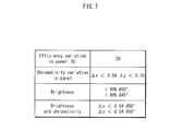
- respective tolerable limits of difference in film thickness of the respective first functional layers of the R, G, and B colors are a range of ⁇ 10 nm to +10 nm, a range of ⁇ 9 nm to +11 nm, and a range of ⁇ 15 nm to +11 nm, respectively.
- Tolerable margin widths of the respective first functional layers of the R, G, and B colors are 20 nm, 20 nm, and 26 nm, respectively
- the “tolerable limits of difference in film thickness” indicate the tolerable limits of difference in film thickness of each layer from the optimal value under the conditions that allowable ranges shown in FIG. 7 are satisfied.
- FIG. 7 shows the following allowable ranges of:
- the “tolerable margin width” indicates a difference between the upper limit and the lower limit in the tolerable limits of difference in film thickness (for example, each layer of the R color in Example 1 has a tolerable margin width of 20 which is the difference between the upper limit of +10 and the lower limit of ⁇ 10).
- the respective hole transport layers of the R, G, and B colors have an optimal film thickness of 20 nm, an optimal film thickness of 9 nm, and an optimal film thickness of 5 nm, respectively.
- the respective organic EL elements of the R, G, and B colors exhibit a light-extraction efficiency of 2.1 cd/A, a light-extraction efficiency of 5.0 cd/A, and a light-extraction efficiency of 0.51 cd/A, respectively.
- the respective organic EL elements of the R, G, and B colors exhibit a chromaticity of (0.66, 0.34), a chromaticity of (0.28, 0.68), and a chromaticity (0.13, 0.06), respectively.
- respective tolerable limits of difference in film thickness of the first functional layers of the R, G, and B colors are a range of ⁇ 11 nm to +9 nm, a range of ⁇ 7 nm to +11 nm, and a range of ⁇ 7 nm to +11 nm, respectively.
- Tolerable margin widths of the first functional layers of the R, G, and B colors are 20 nm, 18 nm, and 18 nm, respectively.
- Example 1 it is possible to exhibit the light-extraction efficiency and the chromaticity that are at the same level as those exhibited in Comparative example 1, and also to set the respective first functional layers of the R, G, and B colors to have the same film thickness. As a result, it is possible to realize both the increase in light-extraction efficiency and the simplification of the manufacturing process.
- each layer constituting the organic EL element should have a film thickness within a range of ⁇ 10% of a film thickness obtained through the simulations in view of manufacturing errors.
- FIG. 8A to FIG. 8C each show the minimum value, the average value, and the maximum value of the film thickness of each layer constituting the organic EL element in Example 1, with respect to the R, G, and B colors, respectively.
- the respective transparent conductive layers of the R, G, and B colors each should have a film thickness of 13.5 nm to 16.5 nm.
- the respective hole injection layers of the R, G, and B colors each should have a film thickness of 4.5 nm to 5.5 nm.
- the respective hole transport layers of the R, G, and B colors each should have a film thickness of 13.5 nm to 16.5 nm.
- the respective electron transport layers of the R, G, and B colors each should have a film thickness of 27 nm to 33 nm.
- the respective organic light-emitting layers of the R, G, and B colors each have an optical distance of 57.6 nm to 70.4 nm from the reflective electrode, and each have an optical distance of 48.6 nm to 59.4 nm from the transparent electrode.
- the respective organic light-emitting layers of the R, G, and B colors should have a film thickness of 81 nm to 99 nm, a film thickness of 63 nm to 77 nm, and a film thickness of 49.5 nm to 60.5 nm, respectively.
- the present inventors further prepared Example 2 and Comparative example 2, and calculated an optimal film thickness of each layer constituting an organic EL element in Example 2 and Comparative example 2 through simulations.
- the second simulations differ from the first simulations in that a reflective electrode and a transparent conductive layer used in the second simulations are formed from an alloy of Al and IZO (Indium Zinc Oxide), respectively.
- FIG. 9A to FIG. 9D show variation of light-extraction efficiency when varying the film thickness of the hole transport layer
- FIG. 9A shows the case where no CF is used in Example 2
- FIG. 9B shows the case where CFs are used in Example 2
- FIG. 9C shows the case where no CF is used in Comparative example 2
- FIG. 10D shows the case where CFs are used in Comparative example 2.
- an electron transport layer of each of the R, G, and B colors has a fixed film thickness of 30 nm
- a hole injection layer of each of the R, G, and B colors has a fixed film thickness of 5 nm
- a transparent conductive layer of each of the R, G, and B colors has a fixed film thickness of 20 nm.
- Respective organic light-emitting layers of the R, G, and B colors have a fixed film thickness of 80 nm, a fixed film thickness of 60 nm, and a fixed film thickness of 20 nm, respectively. The film thickness of only the hole transport layer is varied.
- an electron transport layer of each of the R, G, and B colors has a fixed film thickness of 30 nm
- a hole injection layer of each of the R, G, and B colors has a fixed film thickness of 5 nm
- a transparent conductive layer of each of the R, G, and B colors has a fixed film thickness of 20 nm.
- Respective organic light-emitting layers of the R, G, and B colors have a fixed film thickness of 80 nm, a fixed film thickness of 80 nm, and a fixed film thickness of 60 nm, respectively. The film thickness of only the hole transport layer is varied.
- Example 2 in order to increase the light-extraction efficiency in Example 2, it is optimal for the respective hole transport layers of the R, G, and B colors each to have a film thickness of 25 nm.
- FIG. 9D compared with Example 2, in order to increase the light-extraction efficiency in Comparative example 2, it is optimal for the respective hole transport layers of the R, G, and B colors to have a film thickness of 25 nm, a film thickness of 16 nm, and a film thickness of 9 nm, respectively.
- the respective hole transport layers of the R, G, and B colors differ from one another in Comparative example 2.
- the reason for this is as described in the first simulations.
- the respective organic light-emitting layers of the R, G, and B colors are set to have a film thickness of 80 nm, a film thickness of 60 nm, and a film thickness of 20 nm, respectively, such that the respective hole transport layers of the R, G, and B colors have the same film thickness corresponding to the first local maximum of light-extraction efficiency of a corresponding color in the case where CFs are used.
- the respective organic light-emitting layers of the R, G, and B colors are set to have a film thickness of 80 nm, a film thickness of 80 nm, and a film thickness of 60 nm, respectively, in the same manner as in the first simulations.
- Example 2 in the case where no CF is used, the respective hole transport layers of the R, G, and B colors each have a slightly different film thickness corresponding to the first local maximum of light-extraction efficiency of a corresponding color.
- the respective hole transport layers of the R, G, and B colors have the same film thickness corresponding to the first local maximum of light-extraction efficiency of the corresponding color. In Example 2 in this way, an optimal design is made for the case where CFs are used.
- FIG. 10A and FIG. 10B show light-extraction efficiency and so on when the hole transport layer is set to have an optimal film thickness in Example 2 and Comparative example 2, respectively.
- the respective hole transport layers of the R, G, and B colors each have an optimal film thickness of 25 nm.
- the respective organic EL elements of the R, G, and B colors exhibit a light-extraction efficiency of 1.9 cd/A, a light-extraction efficiency of 4.8 cd/A, and a light-extraction efficiency of 0.51 cd/A, respectively.
- the respective organic EL elements of the R, G, and B colors exhibit a chromaticity of (0.66, 0.34), a chromaticity of (0.28, 0.67), and a chromaticity (0.13, 0.06), respectively.
- respective tolerable limits of difference in film thickness of the respective first functional layers of the R, G, and B colors are a range of ⁇ 13 nm to +13 nm, a range of ⁇ 18 nm to +10 nm, and a range of ⁇ 14 nm to +11 nm, respectively.
- Tolerable margin widths of the respective first functional layers of the R, G, and B colors are 26 nm, 28 nm, and 25 nm, respectively.
- the respective hole transport layers of the R, G, and B colors have an optimal film thickness of 25 nm, an optimal film thickness of 16 nm, and an optimal film thickness of 9 nm, respectively.
- the respective organic EL elements of the R, G, and B colors exhibit a light-extraction efficiency of 1.9 cd/A, a light-extraction efficiency of 4.7 cd/A, and a light-extraction efficiency of 0.49 cd/A, respectively.
- the respective organic EL elements of the R, G, and B colors exhibit a chromaticity of (0.66, 0.34), a chromaticity of (0.28, 0.67), and a chromaticity (0.13, 0.06), respectively.
- respective tolerable limits of difference in film thickness of the respective first functional layers of the R, G, and B colors are a range of ⁇ 13 nm to +13 nm, a range of ⁇ 17 nm to +11 nm, and a range of ⁇ 9 nm to +11 nm, respectively.
- Tolerable margin widths of the respective first functional layers of the R, G, and B colors are 26 nm, 28 nm, and 20 nm, respectively.
- Example 2 it is possible to exhibit the light-extraction efficiency and the chromaticity that are at the same level as those exhibited in Comparative example 2, and also to set the respective first functional layers of the R, G, and B colors to have the same film thickness. As a result, it is possible to realize both the increase in light-extraction efficiency and the simplification of the manufacturing process.
- each layer constituting the organic EL element should have a film thickness within a range of ⁇ 10% of a film thickness obtained through the simulations in view of manufacturing errors.
- FIG. 11A to FIG. 11C each show the minimum value, the average value, and the maximum value of the film thickness of each layer constituting the organic EL element in Example 2, with respect to the R, G, and B colors, respectively.
- the respective transparent conductive layers of the R, G, and B colors each should have a film thickness of 18 nm to 22 nm.
- the respective hole injection layers of the R, G, and B colors each should have a film thickness of 4.5 nm to 5.5 nm.
- the respective hole transport layers of the R, G, and B colors each should have a film thickness of 22.5 nm to 27.5 nm.
- the respective electron transport layers of the R, G, and B colors each should have a film thickness of 27 nm to 33 nm.
- the respective organic light-emitting layers of the R, G, and B colors each have an optical distance of 81.5 nm to 99.6 nm from the reflective electrode, and each have an optical distance of 48.6 nm to 59.4 nm from the transparent electrode.
- FIG. 12A to FIG. 12D show variation of light-extraction efficiency when varying the film thickness of the hole transport layer
- FIG. 12A shows a case where no CF is used in Example 3
- FIG. 12B shows a case where CFs are used in Example 3
- FIG. 12C shows a case where no CF is used in Comparative example 3
- FIG. 12D shows a case where CFs are used in Comparative example 3.
- FIG. 13A to FIG. 13C show variation of chromaticity (x,y) when varying the film thickness of the respective hole transport layers of the R, G, and B colors, respectively.
- FIG. 12A to FIG. 12D prove that when the film thickness of the hole transport layer is varied, the light-extraction efficiency varies.
- FIG. 13A to FIG. 13C prove that when the film thickness of the hole transport layer is varied, the chromaticity varies.
- FIG. 12A to FIG. 12D and FIG. 13A to FIG. 13C prove that a chromaticity corresponding to a local maximum of light-extraction efficiency is not necessarily at the neighborhood of a target chromaticity.
- the respective target chromaticities of the R, G, and B colors are (0.66, 0.34), (0.28, 0.68), and (0.13, 0.06), respectively.
- the substrate 1 is a Thin Film Transistor (TFT) substrate, for example.
- the substrate 1 is a glass plate or quartz plate of soda glass, nonfluorescent glass, phosphate glass, borate glass, or the like; a plastic plate or plastic film of acrylic resin, styrenic resin, polycarbonate resin, epoxy resin, polyethylene, polyester, silicone resin, or the like; or a metal plate or metal foil of alumina or the like.
- the banks 12 should be formed from an insulating material, and it is preferable that the banks 12 have organic solvent resistance. Furthermore, since the banks 12 undergo etching, baking, and the like, it is preferable that the banks 12 be formed from a material that is highly resistant to such processes.
- the material for the banks 12 may be an organic material such as resin, or an inorganic material such as glass.
- acrylic resin, polyimide resin, novolac-type phenolic resin, and the like can be used.
- silicon dioxide (SiO 2 ), silicon nitride (Si 3 N 4 ), and the like can be used.
- the reflective electrode 2 is electrically connected to the TFT provided on the substrate 1 .
- the reflective electrode 2 has the function of reflecting light emitted from the organic light-emitting layers 6 b , 6 g , and 6 r towards the reflective electrode 2 .
- the reflecting function may be achieved by the structural material of the reflective electrode 2 or by applying a reflective coating to the surface portion of the reflective electrode 2 .
- the reflective electrode 2 is formed from Ag (silver), APC (alloy of silver, palladium, and copper), ARA (alloy of silver, rubidium, and gold), MoCr (alloy of molybdenum and chromium), NiCr (alloy of nickel and chromium), or the like.
- the transparent conductive layer 3 functions as a protective layer to prevent the reflective electrode 2 from naturally oxidizing during the manufacturing process.
- the material for the transparent conductive layer 3 should be formed from a conductive material sufficiently translucent with respect to light emitted by the organic light-emitting layers 6 b , 6 g , and 6 r .
- the transparent conductive layer 3 is preferably formed from ITO or IZO, which achieve good conductivity even when a film thereof is formed at room temperature.
- the hole injection layer 4 has the function of injecting holes into the organic light-emitting layers 6 b , 6 g , and 6 r .
- the hole injection layer 4 is formed from an oxide of a transition metal, such as tungsten oxide (WOx), molybdenum oxide (MoOx), and molybdenum tungsten oxide (MoxWyOz).
- tungsten oxide WOx
- MoOx molybdenum oxide
- MoxWyOz molybdenum tungsten oxide
- Forming the hole injection layer 4 from an oxide of a transition metal allows for improvement of voltage-current density characteristics, and for an increase in emission intensity by increasing current density.
- other metal compounds such as a transition metal nitride, may also be used.
- Examples of the material for the hole transport layer 5 include a triazole derivative, an oxadiazole derivative, an imidazole derivative, a polyarylalkane derivative, a pyrazoline derivative and pyrazolone derivative, a phenylenediamine derivative, an arylamine derivative, an amino-substituted chalcone derivative, an oxazole derivative, a styrylanthracene derivative, a fluorenone derivative, a hydrazone derivative, a stilbene derivative, a porphyrin compound, an aromatic tertiary amine compound and styrylamine compound, a butadiene compound, a polystyrene derivative, a hydrazone derivative, a triphenylmethane derivative, or a tetraphenylbenzene derivative, as disclosed in Japanese Patent Application Publication No. 5-163488.
- the organic light-emitting layers 6 b , 6 g , and 6 r are formed from a fluorescent material such as, for example, an oxinoid compound, perylene compound, coumarin compound, azacoumarin compound, oxazole compound, oxadiazole compound, perinone compound, pyrrolo-pyrrole compound, naphthalene compound, anthracene compound, fluorene compound, fluoranthene compound, tetracene compound, pyrene compound, coronene compound, quinolone compound and azaquinolone compound, pyrazoline derivative and pyrazolone derivative, rhodamine compound, chrysene compound, phenanthrene compound, cyclopentadiene compound, stilbene compound, diphenylquinone compound, styryl compound, butadiene compound, dicyanomethylene pyran compound, dicyanomethylene thiopyran compound, fluorescein compound, pyryl
- Examples of the material for the electron transport layer 7 include a nitro-substituted fluorenone derivative, a thiopyran dioxide derivative, a diphenylquinone derivative, a perylene tetracarboxyl derivative, an anthraquinodimethane derivative, a fluoronylidene methane derivative, an anthrone derivative, an oxadiazole derivative, a perinone derivative, and a quinolone complex derivative, as recited in Japanese Patent Application Publication No. H5-163488.
- the above materials for forming the electron transport layer may be doped with an alkali metal or an alkaline-earth metal, such as Na, Ba, or Ca.
- the transparent electrode 8 functions as a negative electrode for the organic EL element.
- the material for the transparent electrode 8 should be formed from a conductive material sufficiently translucent with respect to light emitted by the organic light-emitting layers 6 b , 6 g , and 6 r .
- the transparent electrode 8 is preferably formed from ITO or IZO.
- the thin-film passivation layer 9 has the function of preventing the layers interposed between the substrate 1 and the thin-film passivation layer 9 from being exposed to moisture or air.
- the material for the thin-film passivation layer 9 is, for example, silicon nitride (SiN), silicon oxynitride (SiON), resin, or the like.
- the resin passivation layer 10 has the functions of adhering a back panel, which is composed of the layers from the substrate 1 to the thin-film passivation layer 9 , to the substrate 11 , on which are formed the color filters 13 b , 13 g , and 13 r , and of preventing the layers from being exposed to moisture or air.
- the material for the resin passivation layer 10 is, for example, a resin adhesive or the like.
- the color filters 13 b , 13 g , and 13 r have the function of correcting the chromaticity of light emitted by the organic light-emitting layers.
- FIG. 14 is a functional block showing an organic display device according to the embodiment of the present invention.
- FIG. 15 is an exemplary external diagram showing the organic display device according to the embodiment of the present invention.
- An organic display device 15 includes an organic display panel 16 and a drive control unit 17 that are electrically connected to each other.
- the organic display panel 16 has the pixel structure shown in FIG. 1 .
- the drive control unit 17 includes drive circuits 18 to 21 that apply voltage between the reflective electrode 2 corresponding to each organic EL element and a transparent electrode 8 , and a control circuit 22 that controls operations of the drive circuits 18 to 21 .
- FIG. 16A to FIG. 16D and FIG. 17A to FIG. 17C show a method of manufacturing an organic EL panel according to the embodiment of the present invention.
- reflective electrodes 2 are formed on a substrate 1 by a vapor deposition method, a sputtering method, or the like ( FIG. 16A ).
- transparent conductive layers 3 are formed on the respective reflective electrodes 2 by the vapor deposition method, the sputtering method, or the like ( FIG. 16B ).
- the respective transparent conductive layers 3 of the R, G, and B colors are set to have the same film thickness.
- a hole injection layer 4 for example, is formed by the vapor deposition method, the sputtering method, or the like. Then, banks 12 are formed. Furthermore, on each of the hole injection layers 4 , a hole transport layer 5 , for example, is formed by a printing method such as the inkjet method ( FIG. 16C ).
- the respective hole injection layers 4 of the R, G, and B colors are set to have the same film thickness. Also, the respective hole transport layers 5 of the R, G, and B colors are set to have the same film thickness.
- an electron transport layer 7 is formed by the vapor deposition method, the sputtering method, or the like ( FIG. 17A ).
- the respective electron transport layers 7 of the R, G, and B colors are set to have the same film thickness.
- a transparent electrode 8 is formed by the vapor deposition method, the sputtering method, or the like ( FIG. 17B ).
- the transparent electrode 8 has a film thickness of 90 nm to 110 nm, for example.
- a thin-film passivation layer 9 is formed on the transparent electrode 8 by the vapor deposition method, the sputtering method, or the like, and a substrate 11 in which color filters 13 b , 13 g , and 13 r are formed is adhered thereto using a resin passivation layer 10 ( FIG. 17C ).
- These passivation layers each have a film thickness of 900 nm to 1100 nm, for example.
- the present invention has been described based on the above embodiment, the present invention is not limited to the above embodiment.
- the present invention may include the following modification examples.
- Example 1 the respective first functional layers of the R, G, and B colors each have a film thickness of 31.5 nm to 38.5 nm.
- the present invention is not limited to this. It is considered that the effect of increasing the light-extraction efficiency is exhibited due to the interference phenomenon that occurs between light traveling the first optical path C 1 and light traveling the second optical path C 2 . This leads to an idea that what is important is not the film thickness of the first functional layer, but the optical distance between the organic light-emitting layer and the reflective electrode. Therefore, the respective organic light-emitting layers of the R, G, and B colors each should have an optical distance of 57.6 nm to 70.4 nm from the reflective electrode. As long as this condition is satisfied, the same effect is exhibited even if the film thickness of the first functional layer is varied.
- the respective first functional layers of the R, G, and B colors each have a film thickness of 45 nm to 55 nm.
- the present invention is not limited to this.
- the respective organic light-emitting layers of the R, G, and B colors each should have an optical distance of 81.5 nm to 99.6 nm from the reflective electrode. As long as this condition is satisfied, the same effect is exhibited even if the film thickness of the first functional layer is varied.
- the second functional layer has a film thickness of 27 nm to 33 nm, the present invention is not limited to this similarly.
- the respective organic light-emitting layers of the R, G, and B colors each should have an optical distance of 48.6 nm to 59.4 nm. As long as this condition is satisfied, the same effect is exhibited even if the film thickness of the second functional layer is varied.
- the first functional layer is constituted from the transparent conductive layer, the hole injection layer, and the hole transport layer.
- the first functional layer may not include any one of the transparent conductive layer, the hole injection layer, and the hole transport layer. Further alternatively, the first functional layer may further include another functional layer.
- the second functional layer is constituted from the hole transport layer.
- the second functional layer may further include an electron injection layer, for example.
- the present invention is applicable to organic EL displays and the like.
Landscapes
- Physics & Mathematics (AREA)
- Optics & Photonics (AREA)
- Engineering & Computer Science (AREA)
- Manufacturing & Machinery (AREA)
- Electroluminescent Light Sources (AREA)
Abstract
Description
- [Patent Literature 1] Japanese Patent Application Publication No. 2006-156344
- [Patent Literature 2] Japanese Patent Application Publication No. 2005-317255
- [Patent Literature 3] Japanese Patent Application Publication No. 2005-322435
- [Patent Literature 4] Japanese Patent Application Publication No. 2005-100946
- [Patent Literature 5] Japanese Patent Application Publication No. 2008-41925
- [Patent Literature 6] Japanese Patent Application Publication No. 2006-179780
-
- 1 substrate
- 2 reflective electrode
- 3 transparent conductive layer
- 4 hole injection layer
- 5 hole transport layer
- 6 b, 6 g, and 6 r organic light-emitting layer
- 7 electron transport layer
- 8 transparent electrode
- 9 thin-film passivation layer
- 10 resin passivation layer
- 11 substrate
- 12 bank
- 13 b, 13 g, and 13 r color filter
- 15 organic display device
- 16 organic display panel
- 17 drive control unit
- 18 to 21 drive circuit
- 22 control circuit
Claims (29)
Applications Claiming Priority (1)
| Application Number | Priority Date | Filing Date | Title |
|---|---|---|---|
| PCT/JP2010/006859 WO2012070085A1 (en) | 2010-11-24 | 2010-11-24 | Organic el panel, display device using same, and method for producing organic el panel |
Publications (2)
| Publication Number | Publication Date |
|---|---|
| US20130285023A1 US20130285023A1 (en) | 2013-10-31 |
| US8916862B2 true US8916862B2 (en) | 2014-12-23 |
Family
ID=46145464
Family Applications (1)
| Application Number | Title | Priority Date | Filing Date |
|---|---|---|---|
| US13/819,059 Active US8916862B2 (en) | 2010-11-24 | 2010-11-24 | Organic EL panel, display device using same, and method for producing organic EL panel |
Country Status (3)
| Country | Link |
|---|---|
| US (1) | US8916862B2 (en) |
| JP (1) | JP5753191B2 (en) |
| WO (1) | WO2012070085A1 (en) |
Cited By (2)
| Publication number | Priority date | Publication date | Assignee | Title |
|---|---|---|---|---|
| US20160111674A1 (en) * | 2014-10-21 | 2016-04-21 | Lg Display Co., Ltd. | Organic light emitting diode display device |
| US20190355793A1 (en) * | 2018-05-16 | 2019-11-21 | Samsung Display Co., Ltd. | Display device |
Families Citing this family (9)
| Publication number | Priority date | Publication date | Assignee | Title |
|---|---|---|---|---|
| JP6140970B2 (en) | 2012-10-12 | 2017-06-07 | 三菱電機株式会社 | Display device and manufacturing method thereof |
| KR101429725B1 (en) * | 2012-10-31 | 2014-08-12 | 엘지디스플레이 주식회사 | Organic Light Emitting Display Device and fabricating method of the same |
| JP6111643B2 (en) * | 2012-12-17 | 2017-04-12 | セイコーエプソン株式会社 | ORGANIC ELECTROLUMINESCENCE DEVICE AND ELECTRONIC DEVICE |
| KR102800325B1 (en) * | 2017-02-16 | 2025-04-29 | 삼성디스플레이 주식회사 | Light-emitting display device |
| CN108565350B (en) * | 2018-04-13 | 2019-06-28 | 京东方科技集团股份有限公司 | OLED device, method for manufacturing the same, and display panel |
| CN108682681B (en) * | 2018-05-25 | 2021-03-30 | 京东方科技集团股份有限公司 | Display substrate, method for making the same, and display device |
| CN109713164A (en) * | 2018-12-29 | 2019-05-03 | 武汉天马微电子有限公司 | Display panel and display device |
| CN109742255B (en) * | 2018-12-29 | 2021-04-30 | 武汉天马微电子有限公司 | Display panel and display device |
| US11980046B2 (en) * | 2020-05-27 | 2024-05-07 | Taiwan Semiconductor Manufacturing Company, Ltd. | Method for forming an isolation structure having multiple thicknesses to mitigate damage to a display device |
Citations (63)
| Publication number | Priority date | Publication date | Assignee | Title |
|---|---|---|---|---|
| JPH04137485A (en) | 1990-09-28 | 1992-05-12 | Ricoh Co Ltd | Electroluminesence element |
| JPH04328294A (en) | 1991-04-26 | 1992-11-17 | Pioneer Electron Corp | Organic electroluminescence element |
| JPH05163488A (en) | 1991-12-17 | 1993-06-29 | Konica Corp | Electroluminescent element of organic thin film |
| US5443922A (en) | 1991-11-07 | 1995-08-22 | Konica Corporation | Organic thin film electroluminescence element |
| EP1052708A2 (en) | 1999-05-12 | 2000-11-15 | Pioneer Corporation | Organic electroluminescence multicolor display and method of fabricating the same |
| JP2004014360A (en) | 2002-06-07 | 2004-01-15 | Fuji Electric Holdings Co Ltd | Organic EL device |
| US6737800B1 (en) | 2003-02-18 | 2004-05-18 | Eastman Kodak Company | White-emitting organic electroluminescent device with color filters and reflective layer for causing colored light constructive interference |
| JP2005100946A (en) | 2003-08-18 | 2005-04-14 | Seiko Epson Corp | ORGANIC EL DEVICE, METHOD FOR MANUFACTURING ORGANIC EL DEVICE, AND ELECTRONIC DEVICE |
| JP2005116516A (en) | 2003-09-19 | 2005-04-28 | Sony Corp | Display device and manufacturing method of display device |
| JP2005209421A (en) | 2004-01-21 | 2005-08-04 | Sony Corp | Display device manufacturing method and display device |
| US20050221124A1 (en) | 2004-04-02 | 2005-10-06 | Seok-Hwan Hwang | Fluorene-based compound and organic electroluminescent display device using the same |
| JP2005317255A (en) | 2004-04-27 | 2005-11-10 | Seiko Epson Corp | Electroluminescent element and display element |
| JP2005322435A (en) | 2004-05-06 | 2005-11-17 | Seiko Epson Corp | Electroluminescent element and display element |
| US20050285508A1 (en) | 2004-06-25 | 2005-12-29 | Chi Mei Optoelectronics Corp. | Color organic EL display and fabrication method thereof |
| US20060020136A1 (en) | 2004-07-14 | 2006-01-26 | Seok-Hwan Hwang | Phenylcarbazole compounds and organic electroluminescence devices using the same |
| US20060108919A1 (en) | 2004-11-22 | 2006-05-25 | Seiko Epson Corporation | Electroluminescent device and electronic apparatus |
| US20060115680A1 (en) | 2004-11-29 | 2006-06-01 | Seok-Hwan Hwang | Phenylcarbazole-based compound and organic electroluminescent device employing the same |
| US20060121313A1 (en) | 2004-12-03 | 2006-06-08 | Samsung Sdi Co., Ltd. | Organic light emitting device having cathode including a magnesium-calcium layer and method for fabricating the same |
| JP2006156344A (en) | 2004-09-24 | 2006-06-15 | Semiconductor Energy Lab Co Ltd | Light emitting device |
| JP2006179780A (en) | 2004-12-24 | 2006-07-06 | Canon Inc | Organic light emitting device and display panel |
| US20060232203A1 (en) | 2005-03-25 | 2006-10-19 | Semiconductor Energy Laboratory Co., Ltd. | Light emitting device |
| JP2006303463A (en) | 2005-03-25 | 2006-11-02 | Semiconductor Energy Lab Co Ltd | Light emitting device |
| US20070013282A1 (en) | 2005-07-15 | 2007-01-18 | Satoshi Okutani | Organic el display |
| JP2007027042A (en) | 2005-07-21 | 2007-02-01 | Toshiba Matsushita Display Technology Co Ltd | Organic el display device |
| US20070057264A1 (en) * | 2005-09-12 | 2007-03-15 | Sony Corporation | Display unit and method for fabricating the same |
| US20070102737A1 (en) | 2003-09-19 | 2007-05-10 | Mitsuhiro Kashiwabara | Display unit, method of manufacturing same, organic light emitting unit, and method of manufacturing same |
| US20070131948A1 (en) | 2004-09-24 | 2007-06-14 | Semiconductor Energy Laboratory Co.,Ltd | Light emitting device |
| JP2007157732A (en) | 2007-01-29 | 2007-06-21 | Sony Corp | LIGHT EMITTING ELEMENT AND DISPLAY DEVICE USING THE SAME |
| US20070228367A1 (en) * | 2006-03-29 | 2007-10-04 | Canon Kabushiki Kaisha | Multicolor organic light emitting apparatus |
| US20070231503A1 (en) | 2004-04-02 | 2007-10-04 | Hwang Seok-Hwan | Organic light emitting device and flat panel display device comprising the same |
| JP2007280677A (en) | 2006-04-04 | 2007-10-25 | Seiko Epson Corp | LIGHT EMITTING DEVICE AND ELECTRONIC DEVICE |
| EP1862524A1 (en) | 2006-05-29 | 2007-12-05 | Samsung SDI Co., Ltd. | Organic light emitting device and flat panel display device comprising the same |
| US20070286944A1 (en) * | 2006-06-13 | 2007-12-13 | Itc Inc., Ltd. | Fabrication of full-color oled panel using micro-cavity structure |
| US20080018239A1 (en) * | 2006-07-21 | 2008-01-24 | Sony Corporation | Display and method for manufacturing display |
| US20080030129A1 (en) | 2006-08-07 | 2008-02-07 | Sukekazu Aratani | Organic light-emitting display device and production method of the same |
| JP4046948B2 (en) | 2001-02-26 | 2008-02-13 | 株式会社日立製作所 | Organic light emitting display |
| CN101138107A (en) | 2005-03-11 | 2008-03-05 | 出光兴产株式会社 | Organic electroluminescent color light emitting device |
| US20080107919A1 (en) | 2004-11-29 | 2008-05-08 | Seok-Hwan Hwang | Phenylcarbazole-based compound and organic electroluminescent device employing the same |
| US20080203898A1 (en) * | 2007-02-28 | 2008-08-28 | Seiko Epson Corporation | Display device |
| US20080252206A1 (en) * | 2004-07-22 | 2008-10-16 | Samsung Sdi Co., Ltd. | Organic electroluminescent display device and method for fabricating the same |
| US20080258609A1 (en) | 2006-10-24 | 2008-10-23 | Canon Kabushiki Kaisha | Organic light-emitting device and method for producing the same |
| US20090072709A1 (en) * | 2007-09-18 | 2009-03-19 | Seiko Epson Corporation | Light-emitting device and electronic apparatus |
| US20090081480A1 (en) * | 2005-05-16 | 2009-03-26 | Dai Nippon Printing Co., Ltd. | Method for luminescent layer formation and organic electroluminescent device |
| US20090091238A1 (en) | 2007-10-05 | 2009-04-09 | Cok Ronald S | Led device having improved light output |
| US20090096359A1 (en) * | 2007-10-16 | 2009-04-16 | Sung-Hun Lee | White organic light emitting device and color display apparatus employing the same |
| US20090096358A1 (en) * | 2007-10-10 | 2009-04-16 | Sung-Hun Lee | White organic light emitting device and color display apparatus employing the same |
| US20090278450A1 (en) * | 2008-05-08 | 2009-11-12 | Seiko Epson Corporation | Organic el device, electronic apparatus, and method for manufacturing organic el device |
| CN101582440A (en) | 2008-05-14 | 2009-11-18 | 精工爱普生株式会社 | Light emitting device and electronic apparatus |
| JP2010067482A (en) | 2008-09-11 | 2010-03-25 | Fujifilm Corp | Organic el display |
| JP2010118163A (en) | 2008-11-11 | 2010-05-27 | Seiko Epson Corp | Light-emitting device, and electronic apparatus |
| JP2010251156A (en) | 2009-04-16 | 2010-11-04 | Panasonic Corp | Color organic electroluminescence display device and manufacturing method thereof |
| US7872256B2 (en) | 2006-11-10 | 2011-01-18 | Samsung Mobile Display Co., Ltd. | Organic light emitting display and fabrication method of the same |
| US7915820B2 (en) * | 2006-03-21 | 2011-03-29 | Samsung Electronics Co., Ltd. | Display device and method of manufacturing the same |
| WO2011083515A1 (en) | 2010-01-08 | 2011-07-14 | パナソニック株式会社 | Organic el panel, display device using same, and method for producing organic el panel |
| US20110316414A1 (en) | 2010-06-28 | 2011-12-29 | Panasonic Corporation | Organic light emitting element and manufacturing method of the same, organic display panel, and organic display device |
| US20120025224A1 (en) | 2010-07-27 | 2012-02-02 | Panasonic Corporation | Organic el display panel and method of manufacturing the same |
| US20120099312A1 (en) * | 2009-06-11 | 2012-04-26 | Pioneer Corporation | Light emitting element and display apparatus |
| US20120104423A1 (en) | 2010-08-10 | 2012-05-03 | Panasonic Corporation | Organic light-emitting element, organic light-emitting device, organic display panel, organic display device, and method of manufacturing an organic light-emitting element |
| US20120126272A1 (en) | 2009-09-29 | 2012-05-24 | Panasonic Corporation | Light-emitting element and display device using same |
| US8203158B2 (en) * | 2009-06-24 | 2012-06-19 | Panasonic Corporation | Organic EL display panel |
| US8373170B2 (en) * | 2009-09-08 | 2013-02-12 | Ricoh Company, Ltd. | Display apparatus, manufacturing method thereof, and electronic equipment |
| US20130193419A1 (en) * | 2012-01-31 | 2013-08-01 | Canon Kabushiki Kaisha | Organic electroluminescent element and display apparatus including the same |
| US8766282B2 (en) * | 2012-10-22 | 2014-07-01 | Samsung Display Co., Ltd. | Organic light emitting display with luminescent layers having varying thicknesses to improve color reproducibility |
-
2010
- 2010-11-24 US US13/819,059 patent/US8916862B2/en active Active
- 2010-11-24 WO PCT/JP2010/006859 patent/WO2012070085A1/en not_active Ceased
- 2010-11-24 JP JP2012545533A patent/JP5753191B2/en active Active
Patent Citations (103)
| Publication number | Priority date | Publication date | Assignee | Title |
|---|---|---|---|---|
| JPH04137485A (en) | 1990-09-28 | 1992-05-12 | Ricoh Co Ltd | Electroluminesence element |
| JPH04328294A (en) | 1991-04-26 | 1992-11-17 | Pioneer Electron Corp | Organic electroluminescence element |
| US5443922A (en) | 1991-11-07 | 1995-08-22 | Konica Corporation | Organic thin film electroluminescence element |
| JPH05163488A (en) | 1991-12-17 | 1993-06-29 | Konica Corp | Electroluminescent element of organic thin film |
| EP1052708A2 (en) | 1999-05-12 | 2000-11-15 | Pioneer Corporation | Organic electroluminescence multicolor display and method of fabricating the same |
| JP2000323277A (en) | 1999-05-12 | 2000-11-24 | Pioneer Electronic Corp | Organic electroluminescent multicolor display and method of manufacturing the same |
| US20030044639A1 (en) * | 1999-05-12 | 2003-03-06 | Yoshinori Fukuda | Organic electroluminescence muti-color display and method of fabricating the same |
| US6541130B2 (en) | 1999-05-12 | 2003-04-01 | Pioneer Corporation | Organic electroluminescence multi-color display and method of fabricating the same |
| JP4046948B2 (en) | 2001-02-26 | 2008-02-13 | 株式会社日立製作所 | Organic light emitting display |
| JP2004014360A (en) | 2002-06-07 | 2004-01-15 | Fuji Electric Holdings Co Ltd | Organic EL device |
| JP2004253389A (en) | 2003-02-18 | 2004-09-09 | Eastman Kodak Co | Multicolor organic light emitting display |
| US6737800B1 (en) | 2003-02-18 | 2004-05-18 | Eastman Kodak Company | White-emitting organic electroluminescent device with color filters and reflective layer for causing colored light constructive interference |
| JP2005100946A (en) | 2003-08-18 | 2005-04-14 | Seiko Epson Corp | ORGANIC EL DEVICE, METHOD FOR MANUFACTURING ORGANIC EL DEVICE, AND ELECTRONIC DEVICE |
| US20050099118A1 (en) | 2003-08-18 | 2005-05-12 | Seiko Epson Corporation | Organic EL device, method of manufacturing the same and electronic apparatus |
| US7132789B2 (en) | 2003-08-18 | 2006-11-07 | Seiko Epson Corporation | Organic EL device, method of manufacturing the same and electronic apparatus |
| JP2005116516A (en) | 2003-09-19 | 2005-04-28 | Sony Corp | Display device and manufacturing method of display device |
| US7973319B2 (en) | 2003-09-19 | 2011-07-05 | Sony Corporation | Display unit, method of manufacturing same, organic light emitting unit, and method of manufacturing same |
| US20110241038A1 (en) | 2003-09-19 | 2011-10-06 | Sony Corporation | Display unit, method of manufacturing same, organic light emitting unit, and method of manufacturing same |
| US20070102737A1 (en) | 2003-09-19 | 2007-05-10 | Mitsuhiro Kashiwabara | Display unit, method of manufacturing same, organic light emitting unit, and method of manufacturing same |
| JP2005209421A (en) | 2004-01-21 | 2005-08-04 | Sony Corp | Display device manufacturing method and display device |
| US20120211733A1 (en) | 2004-04-02 | 2012-08-23 | Samsung Mobile Display Co., Ltd. | Organic light emitting device and flat panel display device comprising the same |
| US20070231503A1 (en) | 2004-04-02 | 2007-10-04 | Hwang Seok-Hwan | Organic light emitting device and flat panel display device comprising the same |
| US8188315B2 (en) | 2004-04-02 | 2012-05-29 | Samsung Mobile Display Co., Ltd. | Organic light emitting device and flat panel display device comprising the same |
| US20050221124A1 (en) | 2004-04-02 | 2005-10-06 | Seok-Hwan Hwang | Fluorene-based compound and organic electroluminescent display device using the same |
| US7737627B2 (en) | 2004-04-02 | 2010-06-15 | Samsung Mobile Display Co., Ltd. | Fluorene-based compound and organic electroluminescent display device using the same |
| JP2005317255A (en) | 2004-04-27 | 2005-11-10 | Seiko Epson Corp | Electroluminescent element and display element |
| JP2005322435A (en) | 2004-05-06 | 2005-11-17 | Seiko Epson Corp | Electroluminescent element and display element |
| JP2006012579A (en) | 2004-06-25 | 2006-01-12 | Kyocera Corp | Color organic EL display and manufacturing method thereof |
| US7259514B2 (en) | 2004-06-25 | 2007-08-21 | Chi Mei Optoelectronics Corp. | Color organic EL display and fabrication method thereof |
| US20050285508A1 (en) | 2004-06-25 | 2005-12-29 | Chi Mei Optoelectronics Corp. | Color organic EL display and fabrication method thereof |
| US20060020136A1 (en) | 2004-07-14 | 2006-01-26 | Seok-Hwan Hwang | Phenylcarbazole compounds and organic electroluminescence devices using the same |
| US7431997B2 (en) | 2004-07-14 | 2008-10-07 | Samsung Sdi Co., Ltd. | Phenylcarbazole compounds and organic electroluminescence devices using the same |
| US20080252206A1 (en) * | 2004-07-22 | 2008-10-16 | Samsung Sdi Co., Ltd. | Organic electroluminescent display device and method for fabricating the same |
| US7875893B2 (en) | 2004-09-24 | 2011-01-25 | Semiconductor Energy Laboratory Co., Ltd. | Light emitting device |
| US20110108864A1 (en) | 2004-09-24 | 2011-05-12 | Semiconductor Energy Laboratory Co., Ltd. | Light emitting device |
| JP2006156344A (en) | 2004-09-24 | 2006-06-15 | Semiconductor Energy Lab Co Ltd | Light emitting device |
| US20070131948A1 (en) | 2004-09-24 | 2007-06-14 | Semiconductor Energy Laboratory Co.,Ltd | Light emitting device |
| US20100006872A1 (en) | 2004-09-24 | 2010-01-14 | Semiconductor Energy Laboratory Co., Ltd. | Light emitting device |
| US8188491B2 (en) | 2004-09-24 | 2012-05-29 | Semiconductor Energy Laboratory Co., Ltd. | Light emitting device |
| US7601988B2 (en) | 2004-09-24 | 2009-10-13 | Semiconductor Energy Laboratory Co., Ltd. | Light emitting device |
| US20120205688A1 (en) | 2004-09-24 | 2012-08-16 | Semiconductor Energy Laboratory Co., Ltd. | Light emitting device |
| JP2006173089A (en) | 2004-11-22 | 2006-06-29 | Seiko Epson Corp | EL device and electronic apparatus |
| US20060108919A1 (en) | 2004-11-22 | 2006-05-25 | Seiko Epson Corporation | Electroluminescent device and electronic apparatus |
| US7605535B2 (en) | 2004-11-22 | 2009-10-20 | Seiko Epson Corporation | Electroluminescent device and electronic apparatus |
| US8021764B2 (en) | 2004-11-29 | 2011-09-20 | Samsung Mobile Display Co., Ltd. | Phenylcarbazole-based compound and organic electroluminescent device employing the same |
| US8021765B2 (en) | 2004-11-29 | 2011-09-20 | Samsung Mobile Display Co., Ltd. | Phenylcarbazole-based compound and organic electroluminescent device employing the same |
| US20080107919A1 (en) | 2004-11-29 | 2008-05-08 | Seok-Hwan Hwang | Phenylcarbazole-based compound and organic electroluminescent device employing the same |
| US20060115680A1 (en) | 2004-11-29 | 2006-06-01 | Seok-Hwan Hwang | Phenylcarbazole-based compound and organic electroluminescent device employing the same |
| US20060121313A1 (en) | 2004-12-03 | 2006-06-08 | Samsung Sdi Co., Ltd. | Organic light emitting device having cathode including a magnesium-calcium layer and method for fabricating the same |
| JP2006179780A (en) | 2004-12-24 | 2006-07-06 | Canon Inc | Organic light emitting device and display panel |
| US20090026921A1 (en) | 2005-03-11 | 2009-01-29 | Idemitsu Kosan Co., Ltd. | Organic electroluminescent color light-emitting device |
| CN101138107A (en) | 2005-03-11 | 2008-03-05 | 出光兴产株式会社 | Organic electroluminescent color light emitting device |
| JP2006303463A (en) | 2005-03-25 | 2006-11-02 | Semiconductor Energy Lab Co Ltd | Light emitting device |
| US20060232203A1 (en) | 2005-03-25 | 2006-10-19 | Semiconductor Energy Laboratory Co., Ltd. | Light emitting device |
| US7851989B2 (en) | 2005-03-25 | 2010-12-14 | Semiconductor Energy Laboratory Co., Ltd. | Light emitting device |
| US20110140101A1 (en) | 2005-03-25 | 2011-06-16 | Semiconductor Energy Laboratory Co., Ltd. | Light Emitting Device |
| US20090081480A1 (en) * | 2005-05-16 | 2009-03-26 | Dai Nippon Printing Co., Ltd. | Method for luminescent layer formation and organic electroluminescent device |
| US20070013282A1 (en) | 2005-07-15 | 2007-01-18 | Satoshi Okutani | Organic el display |
| US7960908B2 (en) | 2005-07-15 | 2011-06-14 | Toshiba Matsushita Display Technology Co., Ltd. | Organic EL display |
| JP2007027042A (en) | 2005-07-21 | 2007-02-01 | Toshiba Matsushita Display Technology Co Ltd | Organic el display device |
| US20070057264A1 (en) * | 2005-09-12 | 2007-03-15 | Sony Corporation | Display unit and method for fabricating the same |
| US7915820B2 (en) * | 2006-03-21 | 2011-03-29 | Samsung Electronics Co., Ltd. | Display device and method of manufacturing the same |
| US7518141B2 (en) | 2006-03-29 | 2009-04-14 | Canon Kabushiki Kaisha | Multicolor organic light emitting apparatus |
| US20070228367A1 (en) * | 2006-03-29 | 2007-10-04 | Canon Kabushiki Kaisha | Multicolor organic light emitting apparatus |
| JP2007280677A (en) | 2006-04-04 | 2007-10-25 | Seiko Epson Corp | LIGHT EMITTING DEVICE AND ELECTRONIC DEVICE |
| EP1862524A1 (en) | 2006-05-29 | 2007-12-05 | Samsung SDI Co., Ltd. | Organic light emitting device and flat panel display device comprising the same |
| JP2007318101A (en) | 2006-05-29 | 2007-12-06 | Samsung Sdi Co Ltd | ORGANIC LIGHT EMITTING ELEMENT AND PANEL DISPLAY DEVICE PROVIDED WITH OLED |
| US20070286944A1 (en) * | 2006-06-13 | 2007-12-13 | Itc Inc., Ltd. | Fabrication of full-color oled panel using micro-cavity structure |
| US20080018239A1 (en) * | 2006-07-21 | 2008-01-24 | Sony Corporation | Display and method for manufacturing display |
| JP2008041925A (en) | 2006-08-07 | 2008-02-21 | Hitachi Displays Ltd | Organic light-emitting display device and method for manufacturing the same |
| US8008852B2 (en) | 2006-08-07 | 2011-08-30 | Hitachi Displays, Ltd. | Organic light-emitting display device and production method of the same |
| US20080030129A1 (en) | 2006-08-07 | 2008-02-07 | Sukekazu Aratani | Organic light-emitting display device and production method of the same |
| US20080258609A1 (en) | 2006-10-24 | 2008-10-23 | Canon Kabushiki Kaisha | Organic light-emitting device and method for producing the same |
| US7872256B2 (en) | 2006-11-10 | 2011-01-18 | Samsung Mobile Display Co., Ltd. | Organic light emitting display and fabrication method of the same |
| JP2007157732A (en) | 2007-01-29 | 2007-06-21 | Sony Corp | LIGHT EMITTING ELEMENT AND DISPLAY DEVICE USING THE SAME |
| US20080203898A1 (en) * | 2007-02-28 | 2008-08-28 | Seiko Epson Corporation | Display device |
| US20090072709A1 (en) * | 2007-09-18 | 2009-03-19 | Seiko Epson Corporation | Light-emitting device and electronic apparatus |
| US20090091238A1 (en) | 2007-10-05 | 2009-04-09 | Cok Ronald S | Led device having improved light output |
| US20100231484A1 (en) | 2007-10-05 | 2010-09-16 | Global Oled Technology Llc | Led device having improved light output |
| US7741770B2 (en) | 2007-10-05 | 2010-06-22 | Global Oled Technology Llc | LED device having improved light output |
| WO2009048520A1 (en) | 2007-10-05 | 2009-04-16 | Eastman Kodak Company | Led device having complementary colour subpixel |
| US20090096358A1 (en) * | 2007-10-10 | 2009-04-16 | Sung-Hun Lee | White organic light emitting device and color display apparatus employing the same |
| US20090096359A1 (en) * | 2007-10-16 | 2009-04-16 | Sung-Hun Lee | White organic light emitting device and color display apparatus employing the same |
| JP2009272150A (en) | 2008-05-08 | 2009-11-19 | Seiko Epson Corp | Organic el device, electronic apparatus, and method for manufacturing of organic el device |
| US20090278450A1 (en) * | 2008-05-08 | 2009-11-12 | Seiko Epson Corporation | Organic el device, electronic apparatus, and method for manufacturing organic el device |
| CN101582440A (en) | 2008-05-14 | 2009-11-18 | 精工爱普生株式会社 | Light emitting device and electronic apparatus |
| US20090283786A1 (en) * | 2008-05-14 | 2009-11-19 | Seiko Epson Corporation | Light emitting device and electronic apparatus |
| JP2009277507A (en) | 2008-05-14 | 2009-11-26 | Seiko Epson Corp | Light-emitting apparatus and electronic equipment |
| US8076687B2 (en) | 2008-05-14 | 2011-12-13 | Seiko Epson Corporation | Light emitting device for improving the color purity of emitted light and electronic apparatus |
| JP2010067482A (en) | 2008-09-11 | 2010-03-25 | Fujifilm Corp | Organic el display |
| JP2010118163A (en) | 2008-11-11 | 2010-05-27 | Seiko Epson Corp | Light-emitting device, and electronic apparatus |
| JP2010251156A (en) | 2009-04-16 | 2010-11-04 | Panasonic Corp | Color organic electroluminescence display device and manufacturing method thereof |
| US20120099312A1 (en) * | 2009-06-11 | 2012-04-26 | Pioneer Corporation | Light emitting element and display apparatus |
| US8203158B2 (en) * | 2009-06-24 | 2012-06-19 | Panasonic Corporation | Organic EL display panel |
| US8373170B2 (en) * | 2009-09-08 | 2013-02-12 | Ricoh Company, Ltd. | Display apparatus, manufacturing method thereof, and electronic equipment |
| US20120126272A1 (en) | 2009-09-29 | 2012-05-24 | Panasonic Corporation | Light-emitting element and display device using same |
| WO2011083515A1 (en) | 2010-01-08 | 2011-07-14 | パナソニック株式会社 | Organic el panel, display device using same, and method for producing organic el panel |
| US20120241780A1 (en) | 2010-01-08 | 2012-09-27 | Panasonic Corporation | Organic el panel, display device using same, and method for producing organic el panel |
| US20110316414A1 (en) | 2010-06-28 | 2011-12-29 | Panasonic Corporation | Organic light emitting element and manufacturing method of the same, organic display panel, and organic display device |
| US20120025224A1 (en) | 2010-07-27 | 2012-02-02 | Panasonic Corporation | Organic el display panel and method of manufacturing the same |
| US20120104423A1 (en) | 2010-08-10 | 2012-05-03 | Panasonic Corporation | Organic light-emitting element, organic light-emitting device, organic display panel, organic display device, and method of manufacturing an organic light-emitting element |
| US20130193419A1 (en) * | 2012-01-31 | 2013-08-01 | Canon Kabushiki Kaisha | Organic electroluminescent element and display apparatus including the same |
| US8766282B2 (en) * | 2012-10-22 | 2014-07-01 | Samsung Display Co., Ltd. | Organic light emitting display with luminescent layers having varying thicknesses to improve color reproducibility |
Non-Patent Citations (22)
| Title |
|---|
| Advisory Action from United States Patent and Trademark Office (USPTO) in U.S. Appl. No. 13/488,987, dated May 12, 2014. |
| International Preliminary Report on Patentability in PCT/JP2010/000087, dated Dec. 5, 2011. |
| International Preliminary Report on Patentability in PCT/JP2010/006859, dated Oct. 17, 2012, together with an English language translation thereof. |
| International Preliminary Report on Patentability in PCT/JP2010/006860, dated Oct. 17, 2012, together with an English language translation thereof. |
| International Preliminary Report on Patentability in PCT/JP2010/006861, dated Oct. 22, 2012, together with an English language translation thereof. |
| International Preliminary Report on Patentability in PCT/JP2010/006862, dated Oct. 18, 2012, together with an English language translation thereof. |
| International Search Report and Written Opinion in PCT/JP2010/000087, dated Feb. 2, 2010. |
| International Search Report and Written Opinion in PCT/JP2010/006859, dated Jan. 11, 2011. |
| International Search Report and Written Opinion in PCT/JP2010/006860, dated Jan. 11, 2011. |
| International Search Report and Written Opinion in PCT/JP2010/006861, dated Jan. 11, 2011. |
| International Search Report and Written Opinion in PCT/JP2010/006862, dated Jan. 11, 2011, corrected version. |
| Office Action from the Patent Office of the People's Republic of China in Chinese Patent Application No. 201080059449.5, dated Jun. 13, 2014, together with a partial English language translation thereof. |
| Office Action from U.S. Patent and Trademark Office (USPTO) in U.S. Appl. No. 13/818,797, dated Apr. 14, 2014. |
| Office Action from United States patent and Trademark Office (USPTO) in U.S. Appl. No. 13/488,987, dated Jan. 16, 2014. |
| Office Action from United States patent and Trademark Office (USPTO) in U.S. Appl. No. 13/819,062, dated Feb. 6, 2014. |
| Office Action from United States patent and Trademark Office (USPTO) in U.S. Appl. No. 13/819,066, dated Jan. 10, 2014. |
| Office Action from United States Patent and Trademark Office (USPTO) in U.S. Appl. No. 13/819,066, dated May 6, 2014. |
| U.S. Appl. No. 13/488,987 to Keiko Kurata et al., filed Jun. 5, 2012. |
| U.S. Appl. No. 13/818,797 to Keiko Kurata et al., filed Feb. 25, 2013. |
| U.S. Appl. No. 13/819,062 to Keiko Kurata et al., filed Feb. 26, 2013. |
| U.S. Appl. No. 13/819,066 to Keiko Kurata et al., filed Feb. 26, 2013. |
| United States Office Action in U.S. Appl. No. 13/488,987, dated Jul. 3, 2013. |
Cited By (4)
| Publication number | Priority date | Publication date | Assignee | Title |
|---|---|---|---|---|
| US20160111674A1 (en) * | 2014-10-21 | 2016-04-21 | Lg Display Co., Ltd. | Organic light emitting diode display device |
| US9780319B2 (en) * | 2014-10-21 | 2017-10-03 | Lg Display Co., Ltd. | Organic light emitting diode display device |
| US20190355793A1 (en) * | 2018-05-16 | 2019-11-21 | Samsung Display Co., Ltd. | Display device |
| US11367753B2 (en) * | 2018-05-16 | 2022-06-21 | Samsung Display Co., Ltd. | Display device |
Also Published As
| Publication number | Publication date |
|---|---|
| US20130285023A1 (en) | 2013-10-31 |
| JP5753191B2 (en) | 2015-07-22 |
| WO2012070085A1 (en) | 2012-05-31 |
| JPWO2012070085A1 (en) | 2014-05-19 |
Similar Documents
| Publication | Publication Date | Title |
|---|---|---|
| US8916862B2 (en) | Organic EL panel, display device using same, and method for producing organic EL panel | |
| US8680542B2 (en) | Organic light-emitting element, organic light-emitting device, organic display panel, organic display device, and method of manufacturing an organic light-emitting element | |
| US8907329B2 (en) | Organic el panel, display device using same, and method for producing organic el panel | |
| US8779453B2 (en) | Light-emitting element and display device using same | |
| US8933471B2 (en) | Organic EL panel, display device using same, and method for producing organic EL panel | |
| US10249848B2 (en) | Organic light-emitting panel and method for producing same | |
| US9761638B2 (en) | Organic EL display panel, display device using same, and method for producing organic EL display panel | |
| US9780321B2 (en) | Organic EL display panel, display device incorporating same, and organic EL display panel manufacturing method | |
| US9887250B2 (en) | Organic el display panel with second blue emitter, display device provided therewith, and method for manufacturing organic el display panel | |
| US8853716B2 (en) | Organic EL panel, display device using same, and method for producing organic EL panel | |
| JP2018129265A (en) | Organic el display panel, and method of manufacturing organic el display panel | |
| US9006758B2 (en) | Light-emitting element and display device using same | |
| US8847217B2 (en) | Organic EL panel, display device using same, and method for producing organic EL panel | |
| US11495777B2 (en) | Self-luminous element, self-luminous panel, and self-luminous panel manufacturing method | |
| JP5778799B2 (en) | Organic light emitting device | |
| JP2011034872A (en) | Lighting device | |
| JP2018129264A (en) | Organic EL display panel and organic EL display panel manufacturing method |
Legal Events
| Date | Code | Title | Description |
|---|---|---|---|
| AS | Assignment |
Owner name: PANASONIC CORPORATION, JAPAN Free format text: ASSIGNMENT OF ASSIGNORS INTEREST;ASSIGNORS:KURATA, KEIKO;MATSUSUE, NORIYUKI;YONEDA, KAZUHIRO;SIGNING DATES FROM 20130204 TO 20130206;REEL/FRAME:030399/0213 |
|
| STCF | Information on status: patent grant |
Free format text: PATENTED CASE |
|
| AS | Assignment |
Owner name: JOLED INC, JAPAN Free format text: ASSIGNMENT OF ASSIGNORS INTEREST;ASSIGNOR:PANASONIC CORPORATION;REEL/FRAME:035187/0483 Effective date: 20150105 |
|
| MAFP | Maintenance fee payment |
Free format text: PAYMENT OF MAINTENANCE FEE, 4TH YEAR, LARGE ENTITY (ORIGINAL EVENT CODE: M1551) Year of fee payment: 4 |
|
| MAFP | Maintenance fee payment |
Free format text: PAYMENT OF MAINTENANCE FEE, 8TH YEAR, LARGE ENTITY (ORIGINAL EVENT CODE: M1552); ENTITY STATUS OF PATENT OWNER: LARGE ENTITY Year of fee payment: 8 |
|
| AS | Assignment |
Owner name: INCJ, LTD., JAPAN Free format text: SECURITY INTEREST;ASSIGNOR:JOLED, INC.;REEL/FRAME:063396/0671 Effective date: 20230112 |
|
| AS | Assignment |
Owner name: JOLED, INC., JAPAN Free format text: CORRECTION BY AFFIDAVIT FILED AGAINST REEL/FRAME 063396/0671;ASSIGNOR:JOLED, INC.;REEL/FRAME:064067/0723 Effective date: 20230425 |
|
| AS | Assignment |
Owner name: JDI DESIGN AND DEVELOPMENT G.K., JAPAN Free format text: ASSIGNMENT OF ASSIGNORS INTEREST;ASSIGNOR:JOLED, INC.;REEL/FRAME:066382/0619 Effective date: 20230714 |
|
| AS | Assignment |
Owner name: MAGNOLIA BLUE CORPORATION, JAPAN Free format text: ASSIGNMENT OF ASSIGNORS INTEREST;ASSIGNOR:JDI DESIGN AND DEVELOPMENT G.K.;REEL/FRAME:072039/0656 Effective date: 20250625 |