US8902142B2 - Liquid crystal display and method of driving the same - Google Patents
Liquid crystal display and method of driving the same Download PDFInfo
- Publication number
- US8902142B2 US8902142B2 US12/421,312 US42131209A US8902142B2 US 8902142 B2 US8902142 B2 US 8902142B2 US 42131209 A US42131209 A US 42131209A US 8902142 B2 US8902142 B2 US 8902142B2
- Authority
- US
- United States
- Prior art keywords
- light
- luminance
- image
- gray level
- liquid crystal
- Prior art date
- Legal status (The legal status is an assumption and is not a legal conclusion. Google has not performed a legal analysis and makes no representation as to the accuracy of the status listed.)
- Active, expires
Links
Images


Classifications
-
- G—PHYSICS
- G09—EDUCATION; CRYPTOGRAPHY; DISPLAY; ADVERTISING; SEALS
- G09G—ARRANGEMENTS OR CIRCUITS FOR CONTROL OF INDICATING DEVICES USING STATIC MEANS TO PRESENT VARIABLE INFORMATION
- G09G3/00—Control arrangements or circuits, of interest only in connection with visual indicators other than cathode-ray tubes
- G09G3/20—Control arrangements or circuits, of interest only in connection with visual indicators other than cathode-ray tubes for presentation of an assembly of a number of characters, e.g. a page, by composing the assembly by combination of individual elements arranged in a matrix no fixed position being assigned to or needed to be assigned to the individual characters or partial characters
- G09G3/34—Control arrangements or circuits, of interest only in connection with visual indicators other than cathode-ray tubes for presentation of an assembly of a number of characters, e.g. a page, by composing the assembly by combination of individual elements arranged in a matrix no fixed position being assigned to or needed to be assigned to the individual characters or partial characters by control of light from an independent source
- G09G3/36—Control arrangements or circuits, of interest only in connection with visual indicators other than cathode-ray tubes for presentation of an assembly of a number of characters, e.g. a page, by composing the assembly by combination of individual elements arranged in a matrix no fixed position being assigned to or needed to be assigned to the individual characters or partial characters by control of light from an independent source using liquid crystals
- G09G3/3611—Control of matrices with row and column drivers
-
- G—PHYSICS
- G02—OPTICS
- G02F—OPTICAL DEVICES OR ARRANGEMENTS FOR THE CONTROL OF LIGHT BY MODIFICATION OF THE OPTICAL PROPERTIES OF THE MEDIA OF THE ELEMENTS INVOLVED THEREIN; NON-LINEAR OPTICS; FREQUENCY-CHANGING OF LIGHT; OPTICAL LOGIC ELEMENTS; OPTICAL ANALOGUE/DIGITAL CONVERTERS
- G02F1/00—Devices or arrangements for the control of the intensity, colour, phase, polarisation or direction of light arriving from an independent light source, e.g. switching, gating or modulating; Non-linear optics
- G02F1/01—Devices or arrangements for the control of the intensity, colour, phase, polarisation or direction of light arriving from an independent light source, e.g. switching, gating or modulating; Non-linear optics for the control of the intensity, phase, polarisation or colour
- G02F1/13—Devices or arrangements for the control of the intensity, colour, phase, polarisation or direction of light arriving from an independent light source, e.g. switching, gating or modulating; Non-linear optics for the control of the intensity, phase, polarisation or colour based on liquid crystals, e.g. single liquid crystal display cells
- G02F1/133—Constructional arrangements; Operation of liquid crystal cells; Circuit arrangements
-
- G—PHYSICS
- G09—EDUCATION; CRYPTOGRAPHY; DISPLAY; ADVERTISING; SEALS
- G09G—ARRANGEMENTS OR CIRCUITS FOR CONTROL OF INDICATING DEVICES USING STATIC MEANS TO PRESENT VARIABLE INFORMATION
- G09G3/00—Control arrangements or circuits, of interest only in connection with visual indicators other than cathode-ray tubes
- G09G3/20—Control arrangements or circuits, of interest only in connection with visual indicators other than cathode-ray tubes for presentation of an assembly of a number of characters, e.g. a page, by composing the assembly by combination of individual elements arranged in a matrix no fixed position being assigned to or needed to be assigned to the individual characters or partial characters
- G09G3/34—Control arrangements or circuits, of interest only in connection with visual indicators other than cathode-ray tubes for presentation of an assembly of a number of characters, e.g. a page, by composing the assembly by combination of individual elements arranged in a matrix no fixed position being assigned to or needed to be assigned to the individual characters or partial characters by control of light from an independent source
- G09G3/3406—Control of illumination source
- G09G3/342—Control of illumination source using several illumination sources separately controlled corresponding to different display panel areas, e.g. along one dimension such as lines
-
- G—PHYSICS
- G09—EDUCATION; CRYPTOGRAPHY; DISPLAY; ADVERTISING; SEALS
- G09G—ARRANGEMENTS OR CIRCUITS FOR CONTROL OF INDICATING DEVICES USING STATIC MEANS TO PRESENT VARIABLE INFORMATION
- G09G5/00—Control arrangements or circuits for visual indicators common to cathode-ray tube indicators and other visual indicators
- G09G5/10—Intensity circuits
-
- G—PHYSICS
- G09—EDUCATION; CRYPTOGRAPHY; DISPLAY; ADVERTISING; SEALS
- G09G—ARRANGEMENTS OR CIRCUITS FOR CONTROL OF INDICATING DEVICES USING STATIC MEANS TO PRESENT VARIABLE INFORMATION
- G09G2320/00—Control of display operating conditions
- G09G2320/02—Improving the quality of display appearance
- G09G2320/0271—Adjustment of the gradation levels within the range of the gradation scale, e.g. by redistribution or clipping
- G09G2320/0276—Adjustment of the gradation levels within the range of the gradation scale, e.g. by redistribution or clipping for the purpose of adaptation to the characteristics of a display device, i.e. gamma correction
-
- G—PHYSICS
- G09—EDUCATION; CRYPTOGRAPHY; DISPLAY; ADVERTISING; SEALS
- G09G—ARRANGEMENTS OR CIRCUITS FOR CONTROL OF INDICATING DEVICES USING STATIC MEANS TO PRESENT VARIABLE INFORMATION
- G09G2320/00—Control of display operating conditions
- G09G2320/06—Adjustment of display parameters
- G09G2320/0626—Adjustment of display parameters for control of overall brightness
- G09G2320/064—Adjustment of display parameters for control of overall brightness by time modulation of the brightness of the illumination source
-
- G—PHYSICS
- G09—EDUCATION; CRYPTOGRAPHY; DISPLAY; ADVERTISING; SEALS
- G09G—ARRANGEMENTS OR CIRCUITS FOR CONTROL OF INDICATING DEVICES USING STATIC MEANS TO PRESENT VARIABLE INFORMATION
- G09G2320/00—Control of display operating conditions
- G09G2320/06—Adjustment of display parameters
- G09G2320/0626—Adjustment of display parameters for control of overall brightness
- G09G2320/0646—Modulation of illumination source brightness and image signal correlated to each other
-
- G—PHYSICS
- G09—EDUCATION; CRYPTOGRAPHY; DISPLAY; ADVERTISING; SEALS
- G09G—ARRANGEMENTS OR CIRCUITS FOR CONTROL OF INDICATING DEVICES USING STATIC MEANS TO PRESENT VARIABLE INFORMATION
- G09G2330/00—Aspects of power supply; Aspects of display protection and defect management
- G09G2330/02—Details of power systems and of start or stop of display operation
- G09G2330/021—Power management, e.g. power saving
-
- G—PHYSICS
- G09—EDUCATION; CRYPTOGRAPHY; DISPLAY; ADVERTISING; SEALS
- G09G—ARRANGEMENTS OR CIRCUITS FOR CONTROL OF INDICATING DEVICES USING STATIC MEANS TO PRESENT VARIABLE INFORMATION
- G09G2360/00—Aspects of the architecture of display systems
- G09G2360/16—Calculation or use of calculated indices related to luminance levels in display data
Definitions
- the present invention relates to a liquid crystal display (“LCD”) and a method of driving the LCD, and more particularly, to an LCD having enhanced display quality and reduced power consumption, and a method of driving the LCD.
- LCD liquid crystal display
- a liquid crystal display (“LCD”) generally includes a first display substrate having a plurality of pixel electrodes, a second display substrate having a plurality of common electrodes and a liquid crystal panel having a dielectrically anisotropic liquid crystal layer interposed between the first display substrate and the second display substrate.
- the LCD displays an image by forming an electric field between the pixel electrodes and the common electrodes, adjusting an intensity of the electric field, and thus controlling an amount of light which transmits through the liquid crystal panel based on an alignment of liquid crystal molecules in the liquid crystal layer due to the electric field.
- the LCD is not a self light-emitting display, and the LCD therefore includes a light-emitting unit which provides light to the liquid crystal panel.
- Exemplary embodiments of the present invention provide a liquid crystal display (“LCD”) having enhanced display quality and reduced power consumption. More specifically, the LCD controls a luminance of light provided by a light-emitting unit based on an image displayed on a liquid crystal panel of the LCD.
- LCD liquid crystal display
- Exemplary embodiments of the present invention also provide a method of driving an LCD having enhanced display quality and reduced power consumption.
- an LCD includes: a signal controller which converts a first image signal having a first gray level based on an original gamma coefficient into a second image signal having a second gray level based on a target gamma coefficient; a liquid crystal panel connected to the signal controller and which displays an image based on the second image signal; and a light-emitting unit connected to the signal controller and which provides light to the liquid crystal panel.
- the target gamma coefficient is less than or equal to the original gamma coefficient, and a luminance of the light provided by the light-emitting unit is adjusted by the signal controller to minimize an amount of luminance distortion of the image.
- a method of driving an LCD includes a liquid crystal panel which displays an image, and a light-emitting unit which provides light to the liquid crystal panel.
- the method includes: converting a first image signal having a first gray level based on an original gamma coefficient into a second image signal having a second gray level based on a target gamma coefficient; providing the second image signal to the liquid crystal panel; and adjusting a luminance of the light provided by the light-emitting unit to minimize an amount of luminance distortion of the image.
- the target gamma coefficient less than or equal to the original gamma coefficient.
- FIG. 1 is a block diagram of a liquid crystal display (“LCD”) according to an exemplary embodiment of the present invention
- FIG. 2 is an equivalent circuit diagram of a pixel of a liquid crystal panel of the LCD according to the exemplary embodiment of the present invention shown in FIG. 1 ;
- FIG. 3 is a block diagram of an image signal controller of the LCD according to the exemplary embodiment of the present invention shown in FIG. 1 ;
- FIG. 4 is a graph of grayscale level versus light transmittance showing an original gamma curve and a target gamma curve according to an exemplary embodiment of the present invention
- FIG. 5 is a block diagram of an optical data signal controller of the LCD according to the exemplary embodiment of the present invention shown in FIG. 1 ;
- FIG. 6 is a schematic circuit diagram of a backlight driver and a light-emitting unit of the LCD according to the exemplary embodiment of the present invention shown in FIG. 1 ;
- FIG. 7 is a graph of grayscale level versus number of pixels illustrating histogram information of an image displayed on the LCD according to the exemplary embodiment of the present invention FIG. 1 ;
- FIG. 8 is a graph of dimming level versus image distortion illustrating luminance distortion of the image which has the histogram information shown in FIG. 7 and which is displayed on the LCD according to the exemplary embodiment of the present invention shown in FIG. 1 ;
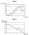
- FIG. 9 is a graph of grayscale level versus number of pixels illustrating histogram information of another image displayed on the LCD according to the exemplary embodiment of the present invention shown in FIG. 1 ;
- FIG. 10 is a graph of dimming level versus image distortion illustrating luminance distortion of the image which has the histogram information shown in FIG. 9 and which is displayed on the LCD according to the exemplary embodiment of the present invention shown in FIG. 1 ;
- FIG. 11 is a block diagram of an LCD and according to an alternative exemplary embodiment of the present invention.
- FIG. 12 is a plan view of a plurality of display blocks and a plurality of light-emitting blocks of the LCD according to the exemplary embodiment of the present invention shown in FIG. 11 ;
- FIG. 13 is a plan view of a plurality of display blocks and a plurality of light-emitting blocks of the LCD according to the exemplary embodiment of the present invention shown in FIG. 11 ;
- FIG. 14 is a schematic circuit diagram of a backlight driver and light-emitting blocks of the LCD according to the exemplary embodiment of the present invention shown in FIG. 11 ;
- FIG. 15 is a block diagram of an LCD according to another alternative exemplary embodiment of the present invention.
- FIG. 16 is a schematic circuit diagram of a plurality of display blocks and a plurality of light-emitting blocks of the LCD according to the exemplary embodiment of the present invention shown in FIG. 15 .
- first,” “second,” “third” etc. may be used herein to describe various elements, components, regions, layers and/or sections, these elements, components, regions, layers and/or sections should not be limited by these terms. These terms are only used to distinguish one element, component, region, layer or section from another element, component, region, layer or section. Thus, a first element, component, region, layer or section discussed below could be termed a second element, component, region, layer or section without departing from the teachings of the present invention.
- relative terms such as “lower” or “bottom” and “upper” or “top” may be used herein to describe one element's relationship to other elements as illustrated in the Figures. It will be understood that relative terms are intended to encompass different orientations of the device in addition to the orientation depicted in the Figures. For example, if the device in one of the figures is turned over, elements described as being on the “lower” side of other elements would then be oriented on the “upper” side of the other elements. The exemplary term “lower” can, therefore, encompass both an orientation of “lower” and “upper,” depending upon the particular orientation of the figure.
- Exemplary embodiments of the present invention are described herein with reference to cross section illustrations which are schematic illustrations of idealized embodiments of the present invention. As such, variations from the shapes of the illustrations as a result, for example, of manufacturing techniques and/or tolerances, are to be expected. Thus, embodiments of the present invention should not be construed as limited to the particular shapes of regions illustrated herein but are to include deviations in shapes which result, for example, from manufacturing. For example, a region illustrated or described as flat may, typically, have rough and/or nonlinear features. Moreover, sharp angles which are illustrated may be rounded. Thus, the regions illustrated in the figures are schematic in nature and their shapes are not intended to illustrate the precise shape of a region and are not intended to limit the scope of the present invention.
- FIG. 1 is a block diagram of an LCD 10 according to an exemplary embodiment of the present invention.
- FIG. 2 is an equivalent circuit diagram of a pixel PX included in a liquid crystal panel 300 of the LCD 10 according to the exemplary embodiment of the present invention shown in FIG. 1 .
- the LCD 10 includes the liquid crystal panel 300 , a signal controller 700 , a grayscale voltage generator 550 , a gate driver 400 , a data driver 500 , a memory 750 , a backlight driver 800 and a light-emitting unit LB connected to the backlight driver 800 .
- the liquid crystal panel 300 includes a plurality of gate lines G 1 through Gk, a plurality of data lines D 1 through Dj and a plurality of the pixels PX.
- the pixels PX include red, green and blue subpixels.
- each of the pixels PX in an LCD according to an exemplary embodiment is disposed in a region where a gate line G of the plurality of gate lines G 1 through Gk and a data line D of the plurality of data lines D 1 through Dj cross each other.
- the liquid crystal panel 300 displays an image based on second image signals R′, G′ and B′ which will be described if further detail below.
- the liquid crystal capacitor Clc includes two electrodes, and, more particularly, a pixel electrode PE of a first display substrate 100 and a common electrode CE of a second display substrate 200 , for example. Liquid crystal molecules 150 are interposed between the pixel electrode PE and the common electrode CE. A color filter CF is formed on a portion of the common electrode CE.
- the signal controller 700 receives first image signals R, G and B and external control signals for controlling display of the first image signals R, G and B. Based on the first image signals R, G and B and the external control signals, the signal controller 700 outputs the second image signals R′, G′ and B′, a data control signal CONT 1 , a gate control signal CONT 2 and an optical data signal LDAT.
- the first image signals have a first gray level which is based on an original gamma coefficient, as well be described in greater detail below.
- the signal controller 700 converts the first image signals R, G and B having the first gray level based on the original gamma coefficient into the second image signals R′, G′ and B′.
- the second image signals R′, G′ and B′ have a second gray level based on a target gamma coefficient, as will be described in greater detail below.
- the target gamma coefficient is less than or equal to the original gamma coefficient.
- the signal controller 700 also provides the optical data signal LDAT to the backlight driver 800 .
- the optical data signal LDAT has a duty ratio which minimizes an amount of image distortion, e.g., luminance distortion, of an image displayed on the liquid crystal panel 300 .
- the signal controller 700 may include an image signal controller 600 _ 1 and an optical data signal controller 600 _ 2 . Further, the image signal controller 600 _ 1 may control the image displayed on the liquid crystal panel 300 , while the optical signal controller 600 _ 2 may control the backlight driver 800 . In addition, the image signal controller 600 _ 1 and the optical data signal controller 600 _ 2 according to an exemplary embodiment of the present invention may be physically separated from each other, but alternative exemplary embodiments are not limited to the functional or physical descriptions described herein.
- the image signal controller 600 _ 1 receives the first image signals R, G and B and outputs the second image signals R′, G′ and B′. Specifically, the image signal controller 600 _ 1 reads the second gray level, which corresponds to the first gray level based on the original gamma coefficient and the target gamma coefficient, respectively, from a lookup table (“LUT”) 760 (described in further detail below) and converts the first image signals R, G and B into the second image signals R′, G′ and B′, respectively. Additionally, the image signal controller 600 _ 1 provides the second image signals R′, G′ and B′ to the data driver 500 , as shown in FIG. 1 .
- LUT lookup table
- the image signal controller 600 _ 1 may receive the external control signals from an external source (not shown) and generate the data control signal CONT 1 and the gate control signal CONT 2 .
- the external control signals include a vertical synchronization signal Vsync, a horizontal synchronization signal Hsync, a main clock signal Mclk and a data enable signal DE, but alternative exemplary embodiments are not limited thereto.
- the data control signal CONT 1 is used to control an operation of the data driver 500
- the gate control signal CONT 2 is used to control an operation of the gate driver 400 .
- the image signal controller 600 _ 1 receives the first image signals R, G and B, extracts numbers of pixels #R, #G and #B at each gray level, and provides the numbers of pixels #R, #G and #B to a histogram information repository 770 .
- the numbers of pixels #R, #G and #B correspond to numbers of the red, green and blue subpixels, respectively, at each gray level of all available gray levels in the image which is displayed on the liquid crystal panel 300 in a given frame.
- the optical data signal controller 600 _ 2 receives information regarding the numbers #R, #G and #B of pixels at each gray level from the histogram information repository 770 , calculates an amount of luminance distortion of an image displayed on the liquid crystal panel 300 , and provides the optical data signal LDAT having the duty ratio which minimizes the amount of luminance distortion to the backlight driver 800 .
- the amount of luminance distortion is an amount of distortion of real luminance of the image displayed on the liquid crystal panel 300 from an ideal luminance corresponding to the original gamma coefficient.
- the amount of luminance distortion, and an operation and structure of the optical data signal controller 600 _ 2 will be described in greater detail below with reference to FIG. 5 .
- the grayscale voltage generator 550 provides a voltage which corresponds to the second image signals R′, G′ and B′ to the data driver 500 .
- the grayscale voltage generator 550 divides a driving voltage AVDD based on the second gray level of the second image signals R′, G′ and B′ and provides the voltages from dividing the driving voltage AVDD to the data driver 500 .
- the grayscale voltage generator 550 may provide the high-level driving voltage AVDD to the data driver 500 .
- the grayscale voltage generator 550 may provide a low-level ground voltage, e.g., 0 V, to the data driver 500 .
- the grayscale voltage generator 550 may include resistors (not shown) connected in series between a node to which the driving voltage AVDD is applied and a ground source to divide the driving voltage AVDD, but alternative exemplary embodiments of the grayscale voltage generator 550 are not limited to the abovementioned description.
- the gate driver 400 receives the gate control signal CONT 2 from the image signal controller 600 _ 1 and transmits a gate signal to the gate lines G 1 through Gk.
- the gate signal includes a gate-on voltage Von and a gate-off voltage Voff provided by a gate on/off voltage generator (not shown).
- the gate control signal CONT 2 controls an operation of the gate driver 400 and may include, for example, a vertical start signal STV ( FIG. 3 ) for starting the operation of the gate driver 400 , a gate clock signal CPV ( FIG. 3 ) for determining when to output the gate-on voltage Von, and an output enable signal OE ( FIG. 3 ) for determining a pulse width of the gate-on voltage Von.
- the data driver 500 receives the data control signal CONT 1 from the image signal controller 600 _ 1 and applies a voltage which corresponds to the second image signals R′, G′ and B′ to the plurality of data lines D 1 through Dj.
- the voltage which corresponds to the second image signals R′, G′ and B′ is provided by the grayscale voltage generator 550 .
- the voltage which corresponds to the second image signals R′, G′ and B′ may be the driving voltage AVDD which has been divided, as described in greater detail above, based on the second gray level of the second image signals R′, G′ and B′.
- the data control signal CONT 1 includes signals used to control an operation of the data driver 500 .
- the signals used to control the operation of the data driver 500 include a horizontal start signal STH ( FIG. 3 ) for starting the operation of the data driver 500 and an output instruction signal TP ( FIG. 3 ) for controlling an output of an image data voltage.
- the memory 750 includes the LUT 760 and the histogram information repository 770 .
- the LUT 760 stores the second gray level of the second image signals R′, G′ and B′ (which corresponds to the first gray level of the first image signals R, G and B).
- the histogram information repository 770 receives information regarding the numbers of pixels #R, #G and #B at each gray level of the image displayed on the liquid crystal panel 300 from the image signal controller 600 _ 1 and stores the information.
- the memory 750 also stores an ideal luminance at each gray level in the LUT 760 .
- the ideal luminance at each gray level is used to calculate the amount of luminance distortion, as will be described in further detail below.
- the amount of luminance distortion can be calculated quickly and efficiently in the LCD 10 according to an exemplary embodiment of the present invention.
- the backlight driver 800 controls a luminance of light which is provided by the light-emitting unit LB based on the optical data signal LDAT. Specifically, the luminance of the light-emitting unit LB is varied according to the duty ratio of the optical data signal LDAT. In addition, the duty ratio of the optical data signal LDAT is adjusted to minimize the amount of luminance distortion of an image displayed on the liquid crystal panel 300 . A structure and operation of the backlight driver 800 will be described in further detail below with reference to FIG. 6 .
- the light-emitting unit LB includes one or more light sources which supply light to the liquid crystal panel 300 .
- the light-emitting unit LB includes a single point light source such as a light-emitting diode (“LED”).
- the light-emitting unit LB may include a line light source or a surface light source, as will be described in further detail below with reference to FIGS. 12 and 13 .
- the luminance of the light-emitting unit LB is controlled by the backlight driver 800 , which is connected to the light-emitting unit LB.
- FIG. 3 is a block diagram of the image signal controller 600 _ 1 of the LCD 10 according to the exemplary embodiment of the present invention shown in shown in FIG. 1 .
- FIG. 4 is a graph of grayscale level versus light transmittance showing an original gamma curve and a target gamma curve according to an exemplary embodiment of the present invention.
- the image signal controller 600 _ 1 includes a control signal generator 610 , a gamma converter 620 and a histogram information extractor 630 .
- the control signal generator 610 receives the external control signals and outputs the data control signal CONT 1 and the gate control signal CONT 2 .
- the control signal generator 610 outputs the vertical start signal STV for starting the gate driver 400 ( FIG. 1 ), the gate clock signal CPV for determining when to output the gate-on voltage Von, the output enable signal OE for determining the pulse width of the gate-on voltage Von, the horizontal start signal STH for starting the data driver 500 ( FIG. 1 ), and the output instruction signal TP for controlling the output of the image data voltage.
- the gamma converter 620 converts the first image signals R, G and B into the second image signals R′, G′ and B′ and outputs the second image signals R′, G′ and B′ to the data driver 500 ( FIG. 1 ).
- the first image signals R, G and B have the first gray level
- the second image signals R′, G′ and B′ have the second gray level, as described in greater detail above.
- the gamma converter 620 converts the first image signals R, G and B into the second image signals R′, G′ and B′ using the LUT 760 which stores the second gray level corresponding to the first gray level based on the target gamma coefficient and the original gamma coefficient, respectively.
- an original gamma curve OG and a target gamma curve TG are plotted according to coordinates including grayscale versus light transmittance.
- an axis which represents the grayscale e.g., the x-axis
- 0 (zero) indicates the lowest gray level
- “max” indicates the highest gray level.
- the original gamma curve OG represents a relationship between each gray level and light transmittance based on the original gamma coefficient.
- the target gamma curve TG represents a relationship between each gray level and light transmittance based on the target gamma coefficient.
- the original gamma coefficient is approximately 2.2, which is known as an ideal gamma coefficient, and the target gamma coefficient in a range from approximately 1.0 to approximately 2.2.
- a corresponding gray level (“output”) corresponding to a corresponding light transmittance which is equal to the specified light transmittance can be found from the original gamma curve OG.
- the specified gray level (input in FIG. 4 ) corresponds to the first gray level
- the gray level (output in FIG. 4 ) on the original gamma curve OG corresponds to the second gray level.
- light transmittance on the target gamma curve TG is greater than a corresponding light transmittance on the original gamma curve OG, as can be seen in FIG. 4 .
- the gamma converter 620 converts the first image signals R, G and B into the second image signals R′, G′ and B′ and outputs the second image signals R′, G′ and B′
- the first image signals R, G and B have the first gray level
- the second image signals R′, G′ and B′ have the second gray level.
- the liquid crystal panel 300 displays an image based on the second image signals R′, G′ and B′.
- a light transmittance of an image displayed on the liquid crystal panel 300 is increased in response to the first image signals R, G and B.
- the histogram information extractor 630 receives the first image signals R, G and B, extracts the numbers of pixels #R, #G and #B at each gray level, and outputs the numbers of pixels #R, #G and #B to the histogram information repository 770 ( FIG. 1 ).
- FIG. 5 is a block diagram of the optical data signal controller 600 _ 2 of the LCD 10 according to the exemplary embodiment of the present invention shown in FIG. 1 .
- the optical data signal controller 600 _ 2 includes a dimming level determiner 660 and a pulse width modulation (“PWM”) signal output unit 670 .
- PWM pulse width modulation
- the dimming level determiner 660 receives the numbers of pixels #R, #G and #B at each gray level from the histogram information repository 770 , and determines a dimming level which minimizes the amount of luminance distortion of the image displayed on the liquid crystal panel 300 .
- the luminance of light provided by the light-emitting unit LB ( FIG. 1 ) is adjusted to minimize the amount of luminance distortion.
- the dimming level according to an exemplary embodiment is defined as a ratio of adjusted luminance of the light to a maximum luminance which can be provided by the light-emitting unit LB.
- the amount of luminance distortion is determined by comparing an ideal luminance at each gray level to a real luminance at each gray level of the image displayed on the liquid crystal panel 300 . Specifically, the amount of luminance distortion is determined based on Equation (1).
- L ideal(i) is ideal luminance at each gray level, e.g., a theoretical luminance when a gamma coefficient is 2.2, e.g., the ideal gamma coefficient
- L real(i) is real luminance, which is reproduced on the liquid crystal panel 300 at each gray level.
- Ni is the number of pixels at each gray level.
- the amount of luminance distortion is equal to a sum of squared products of a number of pixels PX at each gray level of the image and a difference between a real luminance L real(i) and an ideal luminance L ideal(i) at each gray level of the image displayed on the liquid crystal panel 300 in one frame.
- the real luminance Lreal(i) is determined by Equation (2).
- L real(i) BL ⁇ ( T red(i) +T green(i) +T blue(i) ), Equation (2) where T red(i) , T green(i) and T blue(i) are light transmittances of subpixels, e.g., the red, green and blue subpixels, respectively, included in each pixel PX ( FIG. 1 ) at each gray level, and BL is the dimming level of the light-emitting unit LB.
- the real luminance L real(i) reproduced on the liquid crystal panel 300 is obtained by multiplying the dimming level by the sum of respective light transmittances of subpixels.
- the real luminance L real(i) at each gray level of the image is equal to a sum of light transmittances T red(i) , T green(i) and T blue(i) of each of the red, green and the blue subpixels, respectively, multiplied by a ratio of the adjusted luminance of the light to the maximum luminance of the light which can be provided by the light-emitting unit LB (e.g., the dimming level).
- the PWM signal output unit 670 outputs the optical data signal LDAT corresponding to the dimming level provided by the dimming level determiner 660 .
- the optical data signal LDAT is a PWM signal.
- a pulse width of the PWM signal is determined by the dimming level. Specifically, a higher the dimming level corresponds to a higher, e.g., longer, pulse width. Conversely, a lower dimming level corresponds to a lower, e.g., short, pulse width.
- the pulse width of the optical data signal LDAT corresponds to a duty ratio thereof.
- the pulse width of the optical data signal LDAT is increased, e.g., as the duty ratio of the optical data signal LDAT is increased, a luminance of light provided by the light-emitting unit LB increases.
- FIG. 6 is a schematic circuit diagram of the backlight driver 800 and the light-emitting unit LB of the LCD 10 according to the exemplary embodiment of the present invention shown in FIG. 1 .
- the backlight driver 800 includes a switching device 810 and controls the luminance of the light-emitting unit LB based on the optical data signal LDAT.
- the switching device 810 of the backlight driver 800 when the optical data signal LDAT is at a high level, the switching device 810 of the backlight driver 800 is turned on, and a power supply voltage Vin is applied to the light-emitting unit LB. Accordingly, electric current flows through the light-emitting unit LB and an inductor L attached in electrical series with the LEDs of the light-emitting unit LB. As a result, the inductor L stores energy generated by the electric current flowing therethrough.
- the switching device 810 of the backlight driver 800 is turned off, and the light-emitting unit LB, the inductor L, and a diode D thereby form a closed circuit. Accordingly, electric current flows through the closed circuit.
- the energy stored in the inductor L is discharged, thereby reducing an amount of the electric current. Since the duty ratio of the optical data signal LDAT determines a period of time during which the switching device 810 is turned on, the duty ration of the optical data signal LDAT also determines the luminance of the light-emitting unit LB.
- FIG. 7 is a graph of grayscale level versus number of pixels illustrating histogram information of an image displayed on the LCD 10 according to the exemplary embodiment of the present invention shown in FIG. 1 .
- FIG. 8 is a graph of dimming level versus image distortion illustrating luminance distortion of the image which has the histogram information shown in FIG. 7 and which is displayed on the LCD 10 according to the exemplary embodiment of the present invention shown in FIG. 1 .
- FIG. 9 is a graph of grayscale level versus number of pixels illustrating histogram information of another image displayed on the LCD 10 according to the exemplary embodiment of the present invention shown in FIG. 1 .
- FIG. 10 is a graph of dimming level versus image distortion illustrating luminance distortion of the image which has the histogram information shown in FIG. 9 and which is displayed on the LCD 10 according to the exemplary embodiment of the present invention shown in FIG. 1 .
- the histogram information illustrated in FIGS. 7 and 9 is based on an assumption, made only for purposes of illustration herein, that the LCD 10 has 64 gray levels, with a lowest gray level thereof being 0 (zero) and a highest gray level thereof being 63. Further, the histogram information indicates numbers of red (“R”), green (“G”) and blue (“B”) subpixels of a pixel PX at each gray level of the 64 gray levels.
- R red
- G green
- B blue
- the graphs of FIGS. 8 and 10 illustrate the dimming level versus the amount of a luminance distortion, e.g., an image quality distortion, with respect to the original gamma coefficient and the target gamma coefficient.
- a luminance distortion e.g., an image quality distortion
- the amount of luminance distortion is minimum when the dimming level is approximately 0.98, e.g., when a luminance of the light-emitting unit LB is effectively maximum.
- an amount of luminance distortion and more particularly, a minimum amount of luminance distortion, is approximately 34,000.
- the target gamma coefficient is used instead of the original gamma coefficient to display the image of FIG. 7 , e.g., a dark image having the relatively low luminance
- the amount of luminance distortion of the image is substantially reduced in the LCD 10 according to an exemplary embodiment of the present invention. Consequently, a display quality of the LCD 10 is substantially enhanced.
- the dimming level is low, the luminance of the light-emitting unit LB is reduced, which, in turn, reduces power consumption of the light-emitting unit LB. Therefore, when the target gamma coefficient is used instead of the original gamma coefficient, power consumption of the LCD 10 according to an exemplary embodiment is substantially reduced.
- the amount of luminance distortion is effectively minimum when the dimming level is approximately 1, e.g., when the luminance of the light-emitting unit LB is effectively maximum.
- the amount of luminance distortion e.g., the minimum amount of luminance distortion
- the target gamma coefficient 1.8
- the amount of luminance distortion is effectively minimum when the dimming level is approximately 0.97.
- the minimum amount of luminance distortion is approximately 68,432.
- the target gamma coefficient is used instead of the original gamma coefficient to display the image of FIG. 9 , e.g., a bright image having the relatively high luminance
- the amount of luminance distortion is substantially reduced. Consequently, the display quality of the LCD 10 according to an exemplary embodiment is substantially enhanced.
- the dimming level is low, the luminance of the light-emitting unit LB is reduced, which, in turn, reduces the power consumption of the light-emitting unit LB. Therefore, when the target gamma coefficient is used instead of the original gamma coefficient, power consumption of the LCD 10 is substantially reduced.
- first image signals R, G and B having a first gray level with respect to an original gamma coefficient is converted into second image signals R′, G′ and B′ having a second gray level with respect to a target gamma coefficient which is smaller than the original gamma coefficient.
- the second image signals R′, G′ and B′ are provided to a liquid crystal panel 300 , and the liquid crystal panel 300 displays an image in response to the second image signals R′, G′ and B′.
- the amount of luminance distortion is calculated for each frame on which an image is displayed, and a dimming level, which minimizes the amount of luminance distortion, is determined. Accordingly, the luminance of light provided by a light-emitting unit LB is adjusted based on the dimming level. Consequently, as described above, a display quality of the LCD 10 according to an exemplary embodiment is substantially enhanced, and a power consumption thereof is effectively reduced.
- FIG. 11 is a block diagram of an LCD 11 according to an alternative exemplary embodiment of the present invention.
- FIG. 12 is a plan view of a plurality of display blocks DB 1 through DBm and a plurality of light-emitting blocks LB 1 through LBm of the LCD 11 according to the exemplary embodiment of the present invention shown in FIG. 11 .
- FIG. 13 is a plan view of the plurality of display blocks DB 1 through DBm and the plurality of light-emitting blocks LB 1 through LBm according to an alternative exemplary embodiment of the present invention.
- FIG. 12 is a plan view of a plurality of display blocks DB 1 through DBm and a plurality of light-emitting blocks LB 1 through LBm of the LCD 11 according to the exemplary embodiment of the present invention shown in FIG. 11 .
- FIG. 13 is a plan view of the plurality of display blocks DB 1 through DBm and the plurality of light-emitting blocks LB 1 through LBm according to an alternative
- FIG. 14 is a schematic circuit diagram a backlight driver 801 and the plurality of light-emitting blocks LB 1 through LBm of the LCD 11 according to the exemplary embodiment of the present invention shown in FIG. 11 .
- the same or like components to those of previously-described exemplary embodiments are indicated by the same reference numerals, and thus any repetitive detailed description will hereinafter be omitted.
- the LCD 11 includes a liquid crystal panel 301 , a signal controller 701 , a grayscale voltage generator 550 , a gate driver 400 , a data driver 500 , a memory 750 , the backlight driver 801 and light-emitting blocks LB 1 through LBm of the plurality of light-emitting blocks LB 1 through LBm connected to the backlight driver 801 .
- the liquid crystal panel 301 includes display blocks DB 1 through DBm to display an image thereon.
- the display blocks DB 1 through DBm may be arranged in a matrix having one (1) row and m columns, as shown in FIG. 11 , but alternative exemplary embodiments are not limited thereto.
- the display blocks DB 1 through DBm correspond to columns COL of the light-emitting blocks LB 1 through LBm, respectively.
- an i th display block DBi corresponds to an i th light-emitting block LBi.
- the signal controller 701 receives first image signals R, G and B and external control signals for controlling display of the first image signals R, G and B and outputs second image signals R′, G′ and B′, a data control signal CONT 1 , a gate control signal CONT 2 , an image data signal IDAT and first through m th optical data signals LDAT 1 through LDATm.
- the signal controller 701 converts the first image signals R, G and B having a first gray level based on an original gamma coefficient into the second image signals R′, G′ and B′ having a second gray level based on a target gamma coefficient.
- the target gamma coefficient is less than or equal to the original gamma coefficient, as described in greater detail above.
- the signal controller 701 also provides the first through m th optical data signals LDAT 1 through LDATm to the backlight driver 801 .
- the first through m th optical data signals LDAT 1 through LDATm have respective duty ratios which minimize amounts of luminance distortion of images displayed on the display blocks DB 1 through DBm, respectively.
- the signal controller 701 includes an image signal controller 600 _ 1 and an optical data signal controller 601 _ 2 .
- the optical data signal controller 601 _ 2 receives numbers of pixels #R, #G and #B at each gray level from a histogram information repository 770 , calculates an amount of luminance distortion of an image displayed on each of the display blocks DB 1 through DBm, and provides the first through m th optical data signals LDAT 1 through LDATm having duty ratios which minimize the amounts of luminance distortion to the backlight driver 801 .
- the backlight driver 801 controls a luminance of light provided by the light-emitting blocks LB 1 through LBm based on the first through m th optical data signals LDAT 1 through LDATm, respectively.
- the luminances of the light-emitting blocks LB 1 through LBm vary according to duty ratios of the first through m th optical data signals LDAT 1 through LDATm, respectively.
- the duty ratios of the first through m th optical data signals LDAT 1 through LDATm are controlled to minimize the amounts of luminance distortion of images displayed on each of the light-emitting blocks LB 1 through LBm, respectively.
- a structure and operation of the backlight driver 801 according to an exemplary embodiment of the present invention will be described in further detail below with reference to FIG. 14 .
- a light-emitting unit LB includes the light-emitting blocks LB 1 through LBm. Further, the light-emitting blocks LB 1 through LBm are disposed under the liquid crystal panel 301 to provide light to the liquid crystal panel 301 . In addition, the light-emitting blocks LB 1 through LBm may be arranged, for example, in columns COL 1 through COLm, as shown in FIGS. 12 and 13 , but alternative exemplary embodiments are not limited thereto.
- Light sources included in the light-emitting blocks LB 1 through LBm may be arranged under a peripheral edge region of the liquid crystal panel 301 , as shown in FIG. 12 .
- the light sources may be point light sources, such as LEDs, arranged under opposite sides of the liquid crystal panel 301 .
- the light sources included in the light-emitting blocks LB 1 through LBm may be arranged directly under the liquid crystal panel 301 , as shown in FIG. 13 .
- the light sources may be line light sources arranged substantially parallel to each other and disposed under the display blocks DB 1 through DBm.
- the light sources according to an exemplary embodiment of the present invention may be, for example, cold cathode fluorescent lamps (“CCFLs”) or, alternatively, hot fluorescent lamps (“HCFLs”), but alternative exemplary embodiments are not limited thereto.
- FIG. 14 is a schematic circuit diagram of the backlight driver 801 and the light-emitting blocks LB 1 through LBm of the LCD 11 according to the exemplary embodiment of the present invention shown in FIG. 11 .
- the backlight driver 801 includes first through m th switching devices 801 _ 1 through 801 — m and therewith controls luminances of the light-emitting blocks LB 1 through LBm based on the first through m th optical data signals LDAT 1 through LDATm, respectively.
- the same or like components shown in of FIG. 14 as those in FIG. 6 are designated by the same reference characters as in FIG. 6 , and any repetitive detailed description thereof will hereinafter be omitted.
- the liquid crystal panel 301 included in the LCD 11 includes the display blocks DB 1 through DBm, and the light-emitting unit LB includes the light-emitting blocks LB 1 through LBm.
- the light-emitting blocks LB 1 through LBm correspond to the display blocks DB 1 through DBm, respectively, and provide light to the display blocks DB 1 through DBm, respectively.
- the luminance of light provided to each of the display blocks DB 1 through DBm may be adjusted to minimize the amount of luminance distortion of an image displayed on each of the display blocks DB 1 through DBm. Therefore, as described above in further detail with respect to FIGS. 1 through 10 , a display quality of the LCD 11 is effectively enhanced, and a power consumption thereof is substantially reduced.
- FIG. 15 is a block diagram of an LCD 12 according to another alternative exemplary embodiment of the present invention.
- FIG. 16 is a schematic circuit diagram of a plurality of display blocks DB 1 through DB(nxm) and aplurality of light-emitting blocks LB 1 through LB(nxm) of the LCD 12 according to the exemplary embodiment of the present invention shown in FIG. 15 .
- Elements substantially the same as those of previously-described exemplary embodiments are indicated by the same reference numerals, and thus and repetitive description thereof will hereinafter be omitted.
- the LCD 12 includes a liquid crystal panel 302 , a signal controller 702 , a grayscale voltage generator 550 , a gate driver 400 , a data driver 500 , a memory 750 , a plurality of backlight drivers 802 _ 1 through 802 — m, and a light-emitting unit LB connected to backlight drivers 802 _ 1 through 802 — m of the plurality of backlight drivers 802 _ 1 through 802 — m.
- the liquid crystal panel 302 includes display blocks DB 1 through DB(nxm) of the plurality of display blocks DB 1 through DB(nxm) to display an image thereon.
- the display blocks DB 1 through DB(nxm) are arranged in a matrix having n rows and m columns (where n and m are natural numbers).
- the display blocks DB 1 through DB(nxm) correspond to the light-emitting blocks LB 1 through LB(nxm) of the light-emitting unit LB, respectively.
- the signal controller 702 receives first image signals R, G and B and external control signals for controlling display of the first image signals R, G and B and outputs second image signals R′, G′ and B′, a data control signal CONT 1 , a gate control signal CONT 2 , an image data signal IDAT and a plurality of optical data signals LDAT.
- the signal controller 702 converts the first image signals R, G and B having a first gray level based on an original gamma coefficient into the second image signals R′, G′ and B′ having a second gray level based on a target gamma coefficient.
- the target gamma coefficient is less than or equal to the original gamma coefficient.
- the signal controller 702 provides the optical data signals LDAT to the backlight drivers 802 _ 1 through 802 — m.
- optical data signals LDAT of the plurality of optical data signals LDAT have duty ratios which minimize amounts of luminance distortion of images displayed on the display blocks DB 1 through DB(nxm).
- the signal controller 702 includes an image signal controller 600 _ 1 and an optical data signal controller 602 _ 2 .
- the optical data signal controller 602 _ 2 receives numbers of pixels #R, #G and #B at each gray level of the image from a histogram information repository 770 , calculates amounts of luminance distortion of images displayed on the display blocks DB 1 through DB(nxm), and provides the optical data signals LDAT having the duty ratios which minimize the amounts of luminance distortion to the backlight drivers 802 _ 1 through 802 — m, respectively.
- the backlight drivers 802 _ 1 through 802 — m control luminances of light provided by the light-emitting blocks LB 1 through LB(nxm) based on the optical data signals LDAT.
- the luminances of the light-emitting blocks LB 1 through LB(nxm) are controlled by images displayed on the display blocks DB 1 through DB(nxm), respectively.
- the luminances of the light-emitting blocks LB 1 through LB(nxm) vary according to the duty ratios of the optical data signals LDAT.
- the duty ratios of the optical data signals LDAT are controlled to minimize the amounts of luminance distortion of images displayed on the display blocks DB 1 through DB(nxm).
- the light-emitting unit LB includes the light-emitting blocks LB 1 through LB(nxm), as shown in FIG. 16 and may further be disposed under the liquid crystal panel 302 ( FIG. 15 ) to provide the light to the liquid crystal panel 302 .
- the light-emitting blocks LB 1 through LB(nxm) may be arranged, for example, as shown in FIG. 15 , but alternative exemplary embodiments of the present invention are not limited thereto.
- the light-emitting blocks LB 1 through LB(nxm) may be arranged in a matrix having n rows and m columns to correspond to the display blocks DB 1 through DB(nxm), respectively.
- Each of the light-emitting blocks LB 1 through LB(nxm) may include one or more light-emitting devices, such as one or more LEDs, for example.
- the liquid crystal panel 302 included in the LCD 12 includes the display blocks DB 1 through DB(nxm) and the light-emitting unit LB includes the light-emitting blocks LB 1 through LB(nxm) corresponding thereto.
- the light-emitting blocks LB 1 through LB(nxm) correspond to the display blocks DB 1 through DB(nxm), respectively, and thereby provide light to the display blocks DB 1 through DB(nxm), respectively.
- a luminance of the light provided to each of the display blocks DB 1 through DB(nxm) is controlled to minimize an amount of luminance distortion of portions of an image which are displayed on each of the display blocks DB 1 through DB(nxm) top display the image on the LCD 12 according to an exemplary embodiment of the present invention.
- a display quality of an LCD is substantially enhanced, and power consumption thereof is effectively reduced.
Landscapes
- Engineering & Computer Science (AREA)
- Physics & Mathematics (AREA)
- General Physics & Mathematics (AREA)
- Computer Hardware Design (AREA)
- Theoretical Computer Science (AREA)
- Chemical & Material Sciences (AREA)
- Crystallography & Structural Chemistry (AREA)
- Nonlinear Science (AREA)
- Mathematical Physics (AREA)
- Optics & Photonics (AREA)
- Control Of Indicators Other Than Cathode Ray Tubes (AREA)
- Liquid Crystal Display Device Control (AREA)
Abstract
Description
where Lideal(i) is ideal luminance at each gray level, e.g., a theoretical luminance when a gamma coefficient is 2.2, e.g., the ideal gamma coefficient, and Lreal(i) is real luminance, which is reproduced on the
L real(i) =BL×(T red(i) +T green(i) +T blue(i)), Equation (2)
where Tred(i), Tgreen(i) and Tblue(i) are light transmittances of subpixels, e.g., the red, green and blue subpixels, respectively, included in each pixel PX (
Claims (18)
Applications Claiming Priority (2)
| Application Number | Priority Date | Filing Date | Title |
|---|---|---|---|
| KR10-2008-0035658 | 2008-04-17 | ||
| KR20080035658A KR101492530B1 (en) | 2008-04-17 | 2008-04-17 | Liquid crystal display and driving method thereof |
Publications (2)
| Publication Number | Publication Date |
|---|---|
| US20090262057A1 US20090262057A1 (en) | 2009-10-22 |
| US8902142B2 true US8902142B2 (en) | 2014-12-02 |
Family
ID=41200721
Family Applications (1)
| Application Number | Title | Priority Date | Filing Date |
|---|---|---|---|
| US12/421,312 Active 2033-01-29 US8902142B2 (en) | 2008-04-17 | 2009-04-09 | Liquid crystal display and method of driving the same |
Country Status (2)
| Country | Link |
|---|---|
| US (1) | US8902142B2 (en) |
| KR (1) | KR101492530B1 (en) |
Cited By (2)
| Publication number | Priority date | Publication date | Assignee | Title |
|---|---|---|---|---|
| US9846799B2 (en) | 2012-05-18 | 2017-12-19 | Apple Inc. | Efficient texture comparison |
| US11302239B2 (en) | 2015-07-23 | 2022-04-12 | Samsung Display Co., Ltd. | Display apparatus and driving method |
Families Citing this family (7)
| Publication number | Priority date | Publication date | Assignee | Title |
|---|---|---|---|---|
| US8294375B2 (en) * | 2009-10-08 | 2012-10-23 | Intersil Americas Inc | Adaptive PWM controller for multi-phase LED driver |
| TWI424403B (en) * | 2010-02-09 | 2014-01-21 | Chunghwa Picture Tubes Ltd | Voltage regulation method |
| JP5687487B2 (en) * | 2010-12-28 | 2015-03-18 | 株式会社ジャパンディスプレイ | Driving circuit |
| KR102043165B1 (en) * | 2013-01-30 | 2019-11-12 | 삼성디스플레이 주식회사 | Display device |
| CN106782377B (en) * | 2016-12-27 | 2018-01-23 | 惠科股份有限公司 | Liquid crystal display device and driving method thereof |
| CN108492769B (en) * | 2018-03-26 | 2020-08-14 | 京东方科技集团股份有限公司 | Brightness adjustment method and device, and display device |
| CN115019723B (en) * | 2022-06-29 | 2025-07-11 | 京东方科技集团股份有限公司 | Screen display method, screen display device, electronic device, program and medium |
Citations (5)
| Publication number | Priority date | Publication date | Assignee | Title |
|---|---|---|---|---|
| US20020011979A1 (en) * | 2000-07-27 | 2002-01-31 | Hiroyuki Nitta | Liquid crystal driving device for controlling a liquid crystal panel and liquid crystal display apparatus |
| US20060208983A1 (en) * | 2002-11-12 | 2006-09-21 | Seung-Woo Lee | Liquid crystal display and driving method thereof |
| US20070285379A1 (en) * | 2006-06-09 | 2007-12-13 | Samsung Electronics Co., Ltd. | Liquid crystal display and method of adjusting brightness for the same |
| US20080074372A1 (en) * | 2006-09-21 | 2008-03-27 | Kabushiki Kaisha Toshiba | Image display apparatus and image display method |
| US20090015601A1 (en) * | 2007-07-13 | 2009-01-15 | Lg.Philips Lcd Co., Ltd. | Liquid crystal display device and driving method thereof |
Family Cites Families (1)
| Publication number | Priority date | Publication date | Assignee | Title |
|---|---|---|---|---|
| KR100859518B1 (en) * | 2002-05-29 | 2008-09-22 | 삼성전자주식회사 | Apparatus of driving a liquid crystal display |
-
2008
- 2008-04-17 KR KR20080035658A patent/KR101492530B1/en not_active Expired - Fee Related
-
2009
- 2009-04-09 US US12/421,312 patent/US8902142B2/en active Active
Patent Citations (5)
| Publication number | Priority date | Publication date | Assignee | Title |
|---|---|---|---|---|
| US20020011979A1 (en) * | 2000-07-27 | 2002-01-31 | Hiroyuki Nitta | Liquid crystal driving device for controlling a liquid crystal panel and liquid crystal display apparatus |
| US20060208983A1 (en) * | 2002-11-12 | 2006-09-21 | Seung-Woo Lee | Liquid crystal display and driving method thereof |
| US20070285379A1 (en) * | 2006-06-09 | 2007-12-13 | Samsung Electronics Co., Ltd. | Liquid crystal display and method of adjusting brightness for the same |
| US20080074372A1 (en) * | 2006-09-21 | 2008-03-27 | Kabushiki Kaisha Toshiba | Image display apparatus and image display method |
| US20090015601A1 (en) * | 2007-07-13 | 2009-01-15 | Lg.Philips Lcd Co., Ltd. | Liquid crystal display device and driving method thereof |
Cited By (2)
| Publication number | Priority date | Publication date | Assignee | Title |
|---|---|---|---|---|
| US9846799B2 (en) | 2012-05-18 | 2017-12-19 | Apple Inc. | Efficient texture comparison |
| US11302239B2 (en) | 2015-07-23 | 2022-04-12 | Samsung Display Co., Ltd. | Display apparatus and driving method |
Also Published As
| Publication number | Publication date |
|---|---|
| KR101492530B1 (en) | 2015-02-12 |
| US20090262057A1 (en) | 2009-10-22 |
| KR20090110070A (en) | 2009-10-21 |
Similar Documents
| Publication | Publication Date | Title |
|---|---|---|
| US8902142B2 (en) | Liquid crystal display and method of driving the same | |
| US8564507B2 (en) | Display apparatus | |
| US8830158B2 (en) | Method of local dimming a light source, light source apparatus for performing the method, and display apparatus having the light source apparatus | |
| US8228286B2 (en) | Display device having variable backlight and method driving the same | |
| CN104134422B (en) | Organic light emitting diode display and driving method thereof | |
| US8638339B2 (en) | Method for correcting pixel data, and display apparatus for performing the method | |
| US8917229B2 (en) | Display device and method of driving the same | |
| US9035868B2 (en) | Method for driving a light source module and display apparatus for performing the method | |
| US20070152926A1 (en) | Apparatus and method for driving liquid crystal display device | |
| US9099049B2 (en) | Method of dimming backlight assembly | |
| US8482510B2 (en) | Method of driving a light source, light source apparatus for performing the method and display apparatus having the light source apparatus | |
| CN101635126A (en) | Method of boosting a display image, controller unit for performing the method, and display apparatus having the controller unit | |
| US9041745B2 (en) | Method of boosting a local dimming signal, boosting drive circuit for performing the method, and display apparatus having the boosting drive circuit | |
| JP5713871B2 (en) | Liquid crystal display device and driving method thereof | |
| JP2007183545A (en) | Field sequential color liquid crystal display device and driving method thereof | |
| CN101572067B (en) | Method of local dimming a light source, light source apparatus, and display apparatus | |
| US20090262065A1 (en) | Liquid crystal display and method of driving the same | |
| US8471797B2 (en) | Liquid crystal display and method of driving the same | |
| JP2004226981A (en) | Driving apparatus for liquid crystal display device and method for generating digital gradation data based on gradation distribution | |
| CN101436387B (en) | Image processing method for backlight illumination control and device using the method | |
| US8243106B2 (en) | Display device and method of driving the same | |
| KR20020017318A (en) | Liquid crystal display device with a compensating function of brightness deviation | |
| KR101232176B1 (en) | Driving circuit for liquid crystal display device and method for driving the same | |
| KR20070059457A (en) | Driving voltage generation module of liquid crystal display |
Legal Events
| Date | Code | Title | Description |
|---|---|---|---|
| AS | Assignment |
Owner name: SAMSUNG ELECTRONICS CO., LTD., KOREA, REPUBLIC OF Free format text: ASSIGNMENT OF ASSIGNORS INTEREST;ASSIGNORS:YOON, JU-YOUNG;KANG, SEOK-WON;SONG, HEE-KWANG;AND OTHERS;SIGNING DATES FROM 20090226 TO 20090302;REEL/FRAME:022531/0857 Owner name: SAMSUNG ELECTRONICS CO., LTD., KOREA, REPUBLIC OF Free format text: ASSIGNMENT OF ASSIGNORS INTEREST;ASSIGNORS:YOON, JU-YOUNG;KANG, SEOK-WON;SONG, HEE-KWANG;AND OTHERS;REEL/FRAME:022531/0857;SIGNING DATES FROM 20090226 TO 20090302 |
|
| AS | Assignment |
Owner name: SAMSUNG DISPLAY CO., LTD., KOREA, REPUBLIC OF Free format text: ASSIGNMENT OF ASSIGNORS INTEREST;ASSIGNOR:SAMSUNG ELECTRONICS CO., LTD.;REEL/FRAME:029093/0177 Effective date: 20120904 |
|
| STCF | Information on status: patent grant |
Free format text: PATENTED CASE |
|
| FEPP | Fee payment procedure |
Free format text: PAYOR NUMBER ASSIGNED (ORIGINAL EVENT CODE: ASPN); ENTITY STATUS OF PATENT OWNER: LARGE ENTITY |
|
| MAFP | Maintenance fee payment |
Free format text: PAYMENT OF MAINTENANCE FEE, 4TH YEAR, LARGE ENTITY (ORIGINAL EVENT CODE: M1551) Year of fee payment: 4 |
|
| MAFP | Maintenance fee payment |
Free format text: PAYMENT OF MAINTENANCE FEE, 8TH YEAR, LARGE ENTITY (ORIGINAL EVENT CODE: M1552); ENTITY STATUS OF PATENT OWNER: LARGE ENTITY Year of fee payment: 8 |