US8901854B1 - Multi-segment LED driving circuit - Google Patents
Multi-segment LED driving circuit Download PDFInfo
- Publication number
- US8901854B1 US8901854B1 US13/889,535 US201313889535A US8901854B1 US 8901854 B1 US8901854 B1 US 8901854B1 US 201313889535 A US201313889535 A US 201313889535A US 8901854 B1 US8901854 B1 US 8901854B1
- Authority
- US
- United States
- Prior art keywords
- string
- strings
- driving circuit
- led driving
- adjusting part
- Prior art date
- Legal status (The legal status is an assumption and is not a legal conclusion. Google has not performed a legal analysis and makes no representation as to the accuracy of the status listed.)
- Active, expires
Links
- 238000001514 detection method Methods 0.000 claims abstract description 32
- 230000003247 decreasing effect Effects 0.000 claims description 4
- 230000005669 field effect Effects 0.000 claims description 3
- 229910044991 metal oxide Inorganic materials 0.000 claims description 3
- 150000004706 metal oxides Chemical class 0.000 claims description 3
- 239000004065 semiconductor Substances 0.000 claims description 3
- 238000010586 diagram Methods 0.000 description 10
- 230000000694 effects Effects 0.000 description 5
- 230000000630 rising effect Effects 0.000 description 2
- 238000006243 chemical reaction Methods 0.000 description 1
- 230000008878 coupling Effects 0.000 description 1
- 238000010168 coupling process Methods 0.000 description 1
- 238000005859 coupling reaction Methods 0.000 description 1
- 238000005286 illumination Methods 0.000 description 1
- 238000004519 manufacturing process Methods 0.000 description 1
- 230000000704 physical effect Effects 0.000 description 1
Images


Classifications
-
- H05B33/0821—
-
- H—ELECTRICITY
- H05—ELECTRIC TECHNIQUES NOT OTHERWISE PROVIDED FOR
- H05B—ELECTRIC HEATING; ELECTRIC LIGHT SOURCES NOT OTHERWISE PROVIDED FOR; CIRCUIT ARRANGEMENTS FOR ELECTRIC LIGHT SOURCES, IN GENERAL
- H05B45/00—Circuit arrangements for operating light-emitting diodes [LED]
- H05B45/40—Details of LED load circuits
- H05B45/44—Details of LED load circuits with an active control inside an LED matrix
- H05B45/48—Details of LED load circuits with an active control inside an LED matrix having LEDs organised in strings and incorporating parallel shunting devices
-
- H05B33/0824—
Definitions
- the present invention relates to the field of light emitting diode (LED) power source device, and more particularly to a multi-segment LED driving circuit that adjusts the operating status of each LED string according to a change of voltage value of an AC input voltage to achieve the effects of high energy conversion efficiency and high light utilization.
- LED light emitting diode
- LED After LED hits the market by its features of low power consumption and high performance, it is a main subject for related manufacturers to find a way of controlling the illumination brightness, operating efficiency and service life of LED lamps.
- most LED lamps adopt a control circuit with a constant current architecture, and the LEDs are serially connected to an N-type metal oxide semiconductor field effect transistor (N-MOSFET) and a current resistor to restrict a constant drive current passing through the LEDs by the current resistor.
- N-MOSFET N-type metal oxide semiconductor field effect transistor
- the current resistor receives the drive current and has a voltage drop value formed at both ends of the current resistor and fed back to an operational amplifier.
- a negative feedback circuit formed by connecting the operational amplifier, the N-MOSFET and the current resistor is provided for stepping down the voltage at both ends of the current resistor and maintaining the voltage constant and equal to the reference voltage value, so as to maintain the drive current at a constant status.
- the total harmonic distortion (THD) is restricted within a range to facilitate selling the product to markets at different places.
- the present invention provides a multi-segment LED driving circuit used in an AC operating mode for driving a plurality of LEDs to ensure a constant current value of a drive current passing through the LEDs, and the LEDs being divided into a plurality of strings, and having a node between every two adjacent strings, characterized in that the multi-segment LED driving circuit comprises at least one detection part, at least one comparison part and at least one adjusting part, and the detection part is electrically coupled to the strings, the comparison part is electrically coupled to the detection part and the adjusting part, and the adjusting part is electrically coupled to each string; and the detection part detects an input voltage and an output voltage at both ends of each and the next string thereof to form a detected value, and the comparison part compares an operating voltage value fed back by the adjusting part with a reference value to output a driving signal and adjust the adjusting part, so as to control the strings that the drive current is passed and then drive the LEDs to emit light.
- the multi-segment LED driving circuit further comprises a current resistor;
- the detection part is an AND gate, the comparison part is an operational amplifier;
- the adjusting part is an N-type metal oxide semiconductor field effect transistor (N-MOSFET); an input terminal of the AND gate is coupled to an input terminal of each string for receiving an input voltage of the string, and another input terminal of the AND gate is coupled to an output terminal of the next string of the string through an inverter for receiving an output voltage of the next string; and an output terminal of the AND gate is coupled to an enable terminal of the comparison part.
- N-MOSFET N-type metal oxide semiconductor field effect transistor
- a drain of the adjusting part is coupled to a node between each string and the next string thereof; a gate of the adjusting part is coupled to an output terminal of the comparison part; and a source of the adjusting part is coupled to a negative input terminal of the comparison part and the current resistor.
- a positive input terminal of the comparison part receives the reference value. Therefore, the aforementioned components constitute a negative feedback circuit architecture for receiving the drive current passing through each string to form the operating voltage value at both ends and then feeding back the operating voltage value to the operational amplifier.
- the negative and positive input terminals of the operational amplifier have the same voltage value as the reference value based on the physical property of the operational amplifier, so that the voltage value received by the current resistor is always maintained at the reference value to ensure that the drive current is a constant current value.
- the present invention timely detects a change of the voltage value of an external AC power through the simple circuit architecture to adjust the load, so that the LED strings emit light sequentially from top to bottom to maintain a constant current value of the drive current and improve the overall service life and efficiency of the circuit.
- the detection part, the comparison part and the adjusting part can be combined directly into a control unit installed in the circuit, in addition being existed in form of separate electronic components.
- the detection parts are sequentially and electrically coupled to an input terminal and an output terminal of the corresponding string and the next string of the string; and the adjusting parts are sequentially and electrically coupled to the output terminal of the corresponding string.
- the detection part, the comparison part and the adjusting part are combined into a single chip unit which is installed in a control chip, and the control chips are connected in series with each other through a pair of corresponding expansion pins, so that the quantity of control chips can be increased or decreased according to the quantity of strings to meet the actual circuit requirements of the LED lamp and improve the industrial application and economic effect.
- FIG. 1 is a block diagram of a preferred embodiment of the present invention
- FIG. 2 is a circuit diagram of a first implementation mode of a preferred embodiment of the present invention.
- FIG. 3 is a circuit diagram of a second implementation mode of a preferred embodiment of the present invention.
- FIG. 4 is a circuit diagram of a third implementation mode of a preferred embodiment of the present invention.
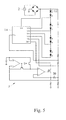
- FIG. 5 is a circuit diagram of a fourth implementation mode of a preferred embodiment of the present invention.
- FIG. 6 is a waveform diagram of the fourth implementation mode of a preferred embodiment of the present invention.
- FIG. 7 is a circuit diagram of a fifth implementation mode of a preferred embodiment of the present invention.
- the multi-segment LED driving circuit 1 comprises a rectifier module 10 , a control module 11 and a plurality of LEDs 12 , and the multi-segment LED driving circuit 1 is used in an AC operating mode for sequentially driving the LEDs 12 to emit light and ensuring a constant current value of a drive current passing through the LEDs 12 .
- the LEDs 12 are divided into a plurality of strings, and a node is formed at a connection position between any two adjacent strings.
- the LEDs 12 are divided sequentially from top to bottom into first and second strings, and a node (V 1 ) is formed between the first and second strings.
- the rectifier circuit 10 can be a bridge rectifier coupled to an external power supply 2 and provided for rectifying an AC voltage into a variable DC voltage to be supplied to the control module 11 and the LEDs 12 .
- the control module 11 has a detection part 110 , a comparison part 111 , an adjusting part 112 and a current resistor (Res) 113 , wherein the detection part 110 is an AND gate, the comparison part 111 is an operational amplifier, and the adjusting part 112 is an N-MOSFET.
- An input terminal of the AND gate is coupled to an output terminal of the rectifier circuit 10 and an input terminal of the first string for receiving an input voltage of the string, and another input terminal of the AND gate is coupled to an output terminal of the next string of the string (which is the second string) through an inverter 1100 for receiving an output voltage of the next string, so that the detection part 110 detects an input voltage and an output voltage at both ends of each string and its next string to form a detected value.
- the N-MOSFET has a drain coupled to the node between each string and its next string, a gate coupled to an output terminal of the operational amplifier, and a source coupled to a negative input terminal of the operational amplifier and the current resistor 113 to constitute a negative feedback circuit architecture, so that the current resistor receives the drive current passing through each string to form an operating voltage value at both ends thereof.
- the positive input terminal of the comparison part 111 receives a reference value (Vref), and the enable terminal is coupled to an output terminal of the AND gate for comparing the operating voltage value fed back by the adjusting part 112 with the reference value when the detected value is received and then outputting a driving signal to adjust the adjusting part 112 , so as to control the drive current passing through the quantity of strings and then sequentially drives the LEDs 12 to emit light.
- Vref a reference value
- the LEDs 12 are divided into S 1 ⁇ S n strings, and nodes V 1 , V 2 , V 3 . . . V n ⁇ 1 are formed between every two adjacent string S 1 and S 2 , S 2 and S 3 , S 3 and S 4 . . . S n ⁇ 1 and S n respectively, and the detection part 110 , the comparison part 111 and the adjusting part 112 are combined to form a control unit.
- an IC with five pins VH, VD 1 , VD 2 , CS and GND is used in the circuit, so that the control module 11 comprises a control unit 13 having IC 1 ⁇ IC n and the current resistor 113 , and an input terminal of the AND gate of the IC 1 is coupled to an output terminal of the rectifier circuit 10 and an input terminal of the first string S 1 through the pin VH, and another input terminal the AND gate of the IC 1 is coupled to an output terminal of the second string S 2 which is the node V 2 in an opposition direction through the pin VD 2 ;
- the N-MOSFET has a drain coupled to the node V 1 through the VD 1 pin, a gate coupled to an output terminal of the operational amplifier, and a source coupled to a negative input terminal of the operational amplifier and coupled to the current resistor 113 through the pin CS.
- An input terminal of the AND gate of the IC 2 is coupled to an input terminal of the second string S 2 through the pin VH; in other words, the node V 2 is coupled to the pin VD 1 of the IC 1 , and another input terminal the AND gate of the IC 2 is coupled to an output terminal of the third string S 3 which is the node V 3 in an opposite direction through the pin VD 2 ; and the N-MOSFET has a drain coupled to the node V 2 through the pin VD 1 , a gate coupled to an output terminal of the operational amplifier, and a source coupled to a negative input terminal of the operational amplifier and coupled to the current resistor 113 through the pin CS, and so on.
- the detection parts 110 of the IC 1 ⁇ IC n are sequentially and electrically coupled to an input terminal of the corresponding string and an output terminal of the next string of the string, and the adjusting parts 112 are sequentially and electrically coupled to an output terminal of the corresponding string.
- the external power supply 2 When the external power supply 2 outputs 110 VAC, the voltage level rises from 0V with time (t) in a sine wave form, the IC 1 obtains appropriate electric energy from the pin VH to start the IC function, and the AND gate obtains a high-level voltage (1). If the voltage inputted by the external power supply 2 does not exceed the total operating critical voltage value of the two LED strings S 1 and S 2 , the pin VD 2 will receive a low-level voltage (0).
- the AND gate inputs the detected value of a high-level voltage to enable the driving signal of a high-level voltage outputted from the operational amplifier to conduct the adjusting part 112 and drive the LEDs 12 of the LED string S 1 to emit light, and the current resistor 113 is provided for controlling the drive current at a constant current value. If the voltage inputted by the external power supply 2 keeps rising and exceeds the total operating critical voltage value of the two LED strings S 1 and S 2 , the LEDs 12 of the LED string S 2 will be conducted, and the pin VH of the IC 2 will obtain appropriate electric energy to start the IC function.
- the drive current passing through S 1 is maintained at V ref /R cs , but the value of the current passing through the S 2 will be increased immediately thereafter, and the value of the current passing into the N-MOSFET of the IC 1 will be decreased.
- the drive current passing through the S 2 is increased gradually such that after the pin VD 2 of the IC 1 receives a high-level voltage (1), the IC 1 will turn off the adjusting part 112 immediately, so that the drive current passes through S 1 and S 2 , and the current is still fixed to V ref /R cs .
- the drive current is a constant current V ref /R cs passing through S 1 +S 2 +S 3 + . . . +S n .
- the strings will conduct the S 1 , S 1 +S 2 , . . . , S 1 +S 2 +S 3 + . . . +S n to emit light sequentially.
- the detection part 110 , the comparison part 111 and the adjusting part 112 are combined into a single chip unit and integrated into a control chip 14 .
- the control chip 14 having two chip units laid therein, so that a drain of a N-MOSFET of a chip unit is coupled to an input terminal of an AND gate of the other chip unit, and then coupled to a pin VD 1 , and an input terminal of the AND gate of the chip unit is coupled to the pin VH, and the other input terminal of the AND gate is coupled to a drain of a N-MOSFET of the other chip unit and then coupled to a pin VD 2 pin, and a pin VD 3 is added for connecting another input terminal of an AND gate of the other chip unit.
- the control chip 14 includes three chip units installed therein and a plurality of pins VD 1 ⁇ VD 4 , and the control chip 14 is installed in a THD correction circuit 3 in an LED lamp as shown in FIG. 5 for controlling the LEDs 12 of the four strings to achieve the effect of increasing or decreasing the drive current with an AC voltage waveform of the external power supply 2 , so as to reduce the THD of the linearly driven circuit of the LED lamp and increase the power factor (PF).
- the THD correction circuit 3 has a compensation resistor 30 with the actually measured signal waveform as shown in FIG. 6 .
- the drive current (ILED_ 1 ) has a current waveform outputted by the LED lamp having the LEDs 12 in a string and without the THD correction circuit 3 and the compensation resistor 30 .
- the drive current (ILED_ 2 ) has a current waveform outputted by the LED lamp having the LEDs 12 with four strings and without the THD correction circuit 3 and the compensation resistor 30 .
- the drive current (ILED_ 3 ) has a current waveform outputted by the LED lamp having the LEDs 12 with four strings and the THD correction circuit 3 but without the compensation resistor 30 .
- the drive current (ILED_ 4 ) has a current waveform outputted by the LED lamp having the LEDs 12 with four strings, the THD correction circuit 3 and the compensation resistor 30 .
- the conduction cycle of the ILED_ 2 is increased, but the current waveform still does not change with the voltage waveform, so that even the THD and PF values are improved, yet they are still not good enough.
- the conduction cycle of the ILED_ 3 is increased and the current waveform changes with the voltage waveform, so that the THD and PF values can be improved significantly.
- the conduction cycle of ILED_ 4 is increased, and the current waveform changes with the voltage waveform.
- the higher the voltage value of the external power supply the greater is the current drop in the conduction cycle. Therefore, the LED lamp can achieve the effect of keeping the input power from being changed severely due to the increase of the input voltage. Therefore, the multi-segment LED driving circuit 1 increases the time for the drive current to be changed with the change of the external power supply 2 , so as to ensure the THD value of the linearly driven circuit at a constant range.
- control module 11 can add another control chip 14 for coupling the newly added four strings, and the two chips can be connected in series with each other through the two pins VCONNECT_O and VCONNECT to simplify the assembly and facilitate the manufacture significantly.
Landscapes
- Circuit Arrangement For Electric Light Sources In General (AREA)
Abstract
Description
Claims (9)
Priority Applications (1)
| Application Number | Priority Date | Filing Date | Title |
|---|---|---|---|
| US13/889,535 US8901854B1 (en) | 2013-05-08 | 2013-05-08 | Multi-segment LED driving circuit |
Applications Claiming Priority (1)
| Application Number | Priority Date | Filing Date | Title |
|---|---|---|---|
| US13/889,535 US8901854B1 (en) | 2013-05-08 | 2013-05-08 | Multi-segment LED driving circuit |
Publications (2)
| Publication Number | Publication Date |
|---|---|
| US20140333215A1 US20140333215A1 (en) | 2014-11-13 |
| US8901854B1 true US8901854B1 (en) | 2014-12-02 |
Family
ID=51864303
Family Applications (1)
| Application Number | Title | Priority Date | Filing Date |
|---|---|---|---|
| US13/889,535 Active 2033-06-26 US8901854B1 (en) | 2013-05-08 | 2013-05-08 | Multi-segment LED driving circuit |
Country Status (1)
| Country | Link |
|---|---|
| US (1) | US8901854B1 (en) |
Cited By (1)
| Publication number | Priority date | Publication date | Assignee | Title |
|---|---|---|---|---|
| US11076465B2 (en) * | 2019-11-29 | 2021-07-27 | Shenzhen Sendis Semiconductor Co., Ltd | Multi-segment linear LED drive circuit, device and driving method |
Families Citing this family (5)
| Publication number | Priority date | Publication date | Assignee | Title |
|---|---|---|---|---|
| TWI538558B (en) * | 2014-06-11 | 2016-06-11 | 立錡科技股份有限公司 | Light emitting device driver circuit and driving method of light emitting device circuit |
| CN105813285A (en) * | 2014-12-31 | 2016-07-27 | 四川新力光源股份有限公司 | LED constant current driving device |
| WO2017036087A1 (en) * | 2015-08-29 | 2017-03-09 | 台州海之大电子科技有限公司 | Led lamp string having selectable light emitting mode |
| CN106658865B (en) * | 2017-01-24 | 2018-05-29 | 苏州智浦芯联电子科技股份有限公司 | LED linear Constant-power drive circuit |
| CN114745829A (en) * | 2022-04-15 | 2022-07-12 | 厦门普为光电科技有限公司 | High-efficiency light-emitting diode driving circuit and high-efficiency light-emitting diode lighting device |
Citations (3)
| Publication number | Priority date | Publication date | Assignee | Title |
|---|---|---|---|---|
| US7999486B2 (en) * | 2008-03-17 | 2011-08-16 | Himax Analogic, Inc. | Driving circuit and method for light emitting diode |
| US8106604B2 (en) * | 2008-03-12 | 2012-01-31 | Freescale Semiconductor, Inc. | LED driver with dynamic power management |
| US8358084B2 (en) * | 2009-11-12 | 2013-01-22 | Green Solution Technology Co., Ltd. | LED current control circuit, current balancer and driving apparatus |
-
2013
- 2013-05-08 US US13/889,535 patent/US8901854B1/en active Active
Patent Citations (3)
| Publication number | Priority date | Publication date | Assignee | Title |
|---|---|---|---|---|
| US8106604B2 (en) * | 2008-03-12 | 2012-01-31 | Freescale Semiconductor, Inc. | LED driver with dynamic power management |
| US7999486B2 (en) * | 2008-03-17 | 2011-08-16 | Himax Analogic, Inc. | Driving circuit and method for light emitting diode |
| US8358084B2 (en) * | 2009-11-12 | 2013-01-22 | Green Solution Technology Co., Ltd. | LED current control circuit, current balancer and driving apparatus |
Cited By (1)
| Publication number | Priority date | Publication date | Assignee | Title |
|---|---|---|---|---|
| US11076465B2 (en) * | 2019-11-29 | 2021-07-27 | Shenzhen Sendis Semiconductor Co., Ltd | Multi-segment linear LED drive circuit, device and driving method |
Also Published As
| Publication number | Publication date |
|---|---|
| US20140333215A1 (en) | 2014-11-13 |
Similar Documents
| Publication | Publication Date | Title |
|---|---|---|
| US9072149B2 (en) | LED driving device with open circuit protection and color temperature and brightness adjustment | |
| TWI435654B (en) | Double-ended current controller and related light-emitting diode lighting device | |
| US8253342B2 (en) | Light emitting diode illumination system | |
| US8901854B1 (en) | Multi-segment LED driving circuit | |
| US9485821B2 (en) | LED lighting drive circuit | |
| US20110115391A1 (en) | Led lamp and led lamp module | |
| TWI425862B (en) | Double-ended current controller and related light-emitting diode lighting device | |
| US20150048744A1 (en) | Light emitting diode driving circuit and light emitting diode illumination apparatus including the same | |
| US9185763B2 (en) | Light emitting diode string driving method | |
| TW201143502A (en) | LED driving circuit and control circuit | |
| GB2525819A (en) | Liquid crystal display, LED backlight source, and driving method thereof | |
| CN104333933A (en) | Light emitting diode driving device and light emitting diode lighting system using same | |
| US20170048944A1 (en) | Lighting apparatus | |
| US9013109B2 (en) | Light-emitting diode lighting device with adjustable current settings and switch voltages | |
| JPWO2017057401A1 (en) | LED drive circuit | |
| CN102006698A (en) | Control method and light emitting device capable of avoiding flicker effect | |
| CN104168688B (en) | Possesses the light emitting diode illuminating apparatus in multiple drive power stage | |
| US9967929B1 (en) | High performance linear LED driving circuit | |
| CN203590567U (en) | AC power supply-based LED drive circuit with function of automatic illumination intensity adjusting | |
| CN102469666B (en) | Feedback Regulator Circuit | |
| TWI499349B (en) | Multi-stage LED driver circuit | |
| CN204559970U (en) | A kind of LED drive chip and BUCK type LED drive circuit | |
| US10201045B1 (en) | Light-emitting diode lighting device | |
| TWI420968B (en) | Led driving circuit and backlight module | |
| TW201433742A (en) | THD improving circuit of LED lamp |
Legal Events
| Date | Code | Title | Description |
|---|---|---|---|
| AS | Assignment |
Owner name: ANWELL SEMICONDUCTOR CORP., TAIWAN Free format text: ASSIGNMENT OF ASSIGNORS INTEREST;ASSIGNORS:CHIU, SHAO-WEI;KUO, CHUN-CHIEH;HSIAO, CHENG-PO;AND OTHERS;REEL/FRAME:030372/0627 Effective date: 20130507 |
|
| STCF | Information on status: patent grant |
Free format text: PATENTED CASE |
|
| MAFP | Maintenance fee payment |
Free format text: PAYMENT OF MAINTENANCE FEE, 4TH YR, SMALL ENTITY (ORIGINAL EVENT CODE: M2551) Year of fee payment: 4 |
|
| AS | Assignment |
Owner name: GIGALINK TECHNOLOGY HOLDING LIMITED, HONG KONG Free format text: ASSIGNMENT OF ASSIGNORS INTEREST;ASSIGNOR:ANWELL SEMICONDUCTOR CORP.;REEL/FRAME:053401/0683 Effective date: 20200728 |
|
| MAFP | Maintenance fee payment |
Free format text: PAYMENT OF MAINTENANCE FEE, 8TH YR, SMALL ENTITY (ORIGINAL EVENT CODE: M2552); ENTITY STATUS OF PATENT OWNER: SMALL ENTITY Year of fee payment: 8 |
|
| AS | Assignment |
Owner name: LEEDARSON LIGHTING CO., LTD, CHINA Free format text: ASSIGNMENT OF ASSIGNORS INTEREST;ASSIGNOR:GIGALINK TECHNOLOGY HOLDING LIMITED;REEL/FRAME:066543/0583 Effective date: 20240220 |