US8895952B2 - Nonvolatile storage device - Google Patents
Nonvolatile storage device Download PDFInfo
- Publication number
- US8895952B2 US8895952B2 US13/404,678 US201213404678A US8895952B2 US 8895952 B2 US8895952 B2 US 8895952B2 US 201213404678 A US201213404678 A US 201213404678A US 8895952 B2 US8895952 B2 US 8895952B2
- Authority
- US
- United States
- Prior art keywords
- memory cell
- electrode
- storage device
- nonvolatile storage
- resistance change
- Prior art date
- Legal status (The legal status is an assumption and is not a legal conclusion. Google has not performed a legal analysis and makes no representation as to the accuracy of the status listed.)
- Active, expires
Links
Images


Classifications
-
- H—ELECTRICITY
- H10—SEMICONDUCTOR DEVICES; ELECTRIC SOLID-STATE DEVICES NOT OTHERWISE PROVIDED FOR
- H10B—ELECTRONIC MEMORY DEVICES
- H10B63/00—Resistance change memory devices, e.g. resistive RAM [ReRAM] devices
- H10B63/80—Arrangements comprising multiple bistable or multi-stable switching components of the same type on a plane parallel to the substrate, e.g. cross-point arrays
- H10B63/84—Arrangements comprising multiple bistable or multi-stable switching components of the same type on a plane parallel to the substrate, e.g. cross-point arrays arranged in a direction perpendicular to the substrate, e.g. 3D cell arrays
-
- H01L27/2481—
-
- H01L27/2409—
-
- H01L45/04—
-
- H01L45/149—
-
- H—ELECTRICITY
- H10—SEMICONDUCTOR DEVICES; ELECTRIC SOLID-STATE DEVICES NOT OTHERWISE PROVIDED FOR
- H10B—ELECTRONIC MEMORY DEVICES
- H10B63/00—Resistance change memory devices, e.g. resistive RAM [ReRAM] devices
- H10B63/20—Resistance change memory devices, e.g. resistive RAM [ReRAM] devices comprising selection components having two electrodes, e.g. diodes
-
- H—ELECTRICITY
- H10—SEMICONDUCTOR DEVICES; ELECTRIC SOLID-STATE DEVICES NOT OTHERWISE PROVIDED FOR
- H10N—ELECTRIC SOLID-STATE DEVICES NOT OTHERWISE PROVIDED FOR
- H10N70/00—Solid-state devices having no potential barriers, and specially adapted for rectifying, amplifying, oscillating or switching
- H10N70/20—Multistable switching devices, e.g. memristors
-
- H—ELECTRICITY
- H10—SEMICONDUCTOR DEVICES; ELECTRIC SOLID-STATE DEVICES NOT OTHERWISE PROVIDED FOR
- H10N—ELECTRIC SOLID-STATE DEVICES NOT OTHERWISE PROVIDED FOR
- H10N70/00—Solid-state devices having no potential barriers, and specially adapted for rectifying, amplifying, oscillating or switching
- H10N70/801—Constructional details of multistable switching devices
- H10N70/821—Device geometry
- H10N70/826—Device geometry adapted for essentially vertical current flow, e.g. sandwich or pillar type devices
-
- H—ELECTRICITY
- H10—SEMICONDUCTOR DEVICES; ELECTRIC SOLID-STATE DEVICES NOT OTHERWISE PROVIDED FOR
- H10N—ELECTRIC SOLID-STATE DEVICES NOT OTHERWISE PROVIDED FOR
- H10N70/00—Solid-state devices having no potential barriers, and specially adapted for rectifying, amplifying, oscillating or switching
- H10N70/801—Constructional details of multistable switching devices
- H10N70/881—Switching materials
- H10N70/884—Switching materials based on at least one element of group IIIA, IVA or VA, e.g. elemental or compound semiconductors
- H10N70/8845—Carbon or carbides
Definitions
- Embodiments described herein relate to a nonvolatile storage device.
- NAND-type flash memories and small hard disk drives (HDD) are widely used as the recording density increases.
- a memory cell is constituted by a resistance change layer and electrodes sandwiching the resistance change layer.
- the resistance change layer stores two or more different electric resistance states, such as a low resistance state and a high resistance state, in a nonvolatile manner. That is, the resistance state of the resistance change layer is changed by applying voltage, current, charge, heat or the like, which is equal to or more than a threshold value, to the electrodes, whereby difference in the resistance value is recorded in association with data.
- the resistance change-type nonvolatile memory has a feature of capable of reading data in a nondestructive manner.
- binary metal oxides such as nickel oxide (NiO) and multicomponent metal oxides such as strontium zirconium oxide (SrZrO 3 ) have been actively researched and developed as materials of resistance change-type memory devices.
- NiO nickel oxide
- SrZrO 3 strontium zirconium oxide
- Materials suitable for the resistance change layer have been searched for, but a suitable material has not yet been found.
- Carbon materials are also considered as candidates for the resistance change layer, and materials and production methods therefor have been researched.
- the carbon material is constituted by a single carbon, and therefore, the composition can be controlled relatively easily with less dependence on process conditions, and there is an advantage in that the control is easy.
- a carbon nano material is also a candidate for the resistance change memory device.
- the carbon nano material is a generic term meaning carbon materials having a three-dimensional structure such as carbon nanotube and fullerene.
- the layer in which the carbon nano material is laminated is different from a bulk film formed as a uniform film in that the layer with the carbon nano material has a three-dimensional structure in which minute tubes are stacked and there is much space, and therefore, a current path is spacially-limited. Therefore, even though the carbon nano material itself is a conductive material, a small current flows in the carbon nano material layer, making it possible to reduce the current required to change the electric resistance state of the carbon nano material layer.
- the mechanism of change of the resistance in the carbon nano material layer has not yet been revealed in detail.
- the resistance change-type memory using the carbon nano material has a possibility of reducing the current required to change the electric resistance state. Therefore, the resistance change-type memory using the carbon nano material attracts attention.
- FIG. 1 is a block diagram illustrating a configuration of a nonvolatile storage device according to a first embodiment of the present invention
- FIG. 2 is a perspective view illustrating a portion of a memory cell array of the nonvolatile storage device according to the embodiment
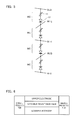
- FIG. 3 is a cross sectional view illustrating a portion of the memory cell array of the nonvolatile storage device according to the embodiment
- FIG. 4 is a cross sectional view illustrating a configuration of a memory cell of the nonvolatile storage device according to the embodiment
- FIG. 5 is a figure illustrating an equivalent circuit of a portion of the memory cell array of the nonvolatile storage device according to the embodiment
- FIG. 6 is a schematic cross sectional view illustrating a device configuration of an experiment sample used in an experiment by the present inventors
- FIG. 7 is a table illustrating a switch operation characteristic of the experiment sample
- FIGS. 8A and 8B are schematic views for explaining a voltage application method for the experiment sample
- FIG. 9 is a table illustrating the relationship between the polarity and the switch operation characteristic of the experiment sample.
- FIG. 10 shows a result of XPS analysis of an interface between a resistance change layer and a lower electrode of the experiment sample
- FIG. 11 is a cross sectional view illustrating a configuration of a variable resistance device in the nonvolatile storage device according to the first embodiment of the present invention.
- FIG. 12 is a cross sectional view illustrating a configuration of a variable resistance device in a nonvolatile storage device according to a second embodiment of the present invention.
- FIG. 13 is a cross sectional view illustrating a configuration of a variable resistance device in a nonvolatile storage device according to a third embodiment of the present invention.
- a nonvolatile storage device is formed by laminating a plurality of memory cell arrays, the memory cell array including a plurality of word lines arranged in parallel, a plurality of bit lines arranged in parallel and crossing these word lines, and memory cells each connected between a word line and a bit line at a crossing portion between the word line and the bit line, the plurality of memory cell arrays being laminated in such a manner as to share adjacent word lines and bit lines, wherein the memory cell includes a current rectifying device and a variable resistance device connected in series, the current rectifying devices provided adjacent to each other in a laminating direction pass currents in directions opposite to each other, the variable resistance device includes a lower electrode, an upper electrode, and a resistance change layer including a conductive nano material formed between the lower electrode and the upper electrode, one of the variable resistance devices provided adjacent to each other in the laminating direction has titanium oxide (TiOx) between the resistance change layer and the lower electrode serving as a cathode, the other of the variable resistance devices provided adjacent
- FIG. 1 is a block diagram illustrating a configuration of a nonvolatile semiconductor storage device according to the first embodiment of the present invention.
- This nonvolatile semiconductor storage device includes a memory cell array 1 in which memory cells MC having variable resistance devices and current rectifying devices described later are arranged in a matrix form.
- a column control circuit 2 is electrically connected to bit lines BL of the memory cell array 1 .
- the column control circuit 2 controls the bit lines BL of the memory cell array 1 , and enables data erase operation of a memory cell, data write operation to a memory cell, and data read operation from a memory cell.
- a row control circuit 3 is electrically connected to word lines WL of the memory cell array 1 .
- the row control circuit 3 selects the word lines WL of the memory cell array 1 , and enables data erase operation of a memory cell, data write operation to a memory cell, and data read operation from a memory cell.
- FIG. 2 is a perspective view illustrating a portion of the memory cell array 1 .
- FIG. 3 is a cross sectional view illustrating one column of the memory cell seen in an arrow direction taken along line I-I′ in FIG. 2 .
- FIG. 4 is a cross sectional view illustrating one memory cell.
- FIG. 5 is an equivalent circuit diagram of the memory cell array illustrated in FIG. 3 .
- the memory cell array 1 is a cross point-type memory cell array. In the memory cell array 1 , the plurality of word lines WL are arranged in parallel, and the plurality of bit lines BL crossing the word lines WL are arranged in parallel.
- a memory cell MC described later is arranged at each crossing portion of the word line WL and the bit line BL such that the memory cell MC is sandwiched between both of the wires.
- Such memory cell arrays MA 0 to MA 3 are formed as a multilayer with adjacent word lines WL and bit lines BL being shared. It should be noted that the word lines WL and the bit lines BL are desirably made of a material with a high degree of heat resistance and a low resistance value.
- Examples of such materials include tungsten (W), titanium (Ti), tungsten nitride (WN), titanium nitride (TiN), tungsten silicide (WSi), nickel silicide (NiSi), cobalt silicide (CoSi), tantalum nitride (TaN), and impurity doped Polysilicon.
- the memory cell MC includes a variable resistance device 11 and a current rectifying device 12 connected in series between the word line WL and the bit line BL.
- the sizes of peripheral circuits connected to the bit line BL and the word line WL crossing each other can be reduced when the bit line BL and the word line WL are configured to be specialized in particular functions different from each other. Therefore, a smaller memory device having the same memory capacity can be achieved.
- the current rectifying direction is different depending on whether the bit line BL is located above or below the word line WL.
- the current rectifying device 12 desirably has such current rectifying characteristics that the current flowed from the bit line BL to the word line WL is larger than the current flowed from the word line WL to the bit line BL in the selected memory cell MC.
- a cathode/anode of the current rectifying devise 12 is defined by a bias applied direction in a reset operation.
- the materials, the structure, and the like of the current rectifying device 12 used in the memory cell MC are not particularly limited as long as the current rectifying device 12 has predetermined current rectifying characteristics with regard to voltage/current characteristics.
- the current rectifying device 12 may be a diode produced from polysilicon (Poly-Si). Examples of the diode include a PN junction diode including a p-type layer and an n-type layer containing impurities.
- the diode is not limited to the PN junction diode, and other examples of the diode include a Schottky diode, various kinds of diodes such as a PIN diode having an i layer not containing any impurity inserted between a p-type layer and an n-type layer, and a punch-through diode.
- the material of the current rectifying device 12 is not limited to silicon (Si).
- the material of the current rectifying device 12 may also be a semiconductor such as silicon germanium (SiGe) and germanium (Ge), a mixed crystal of semiconductor and metal, or an insulating material such as an oxide, so that the current rectifying device 12 has such current rectifying characteristics that desired voltage and current are provided to the resistance change layer of the selected memory cell MC.
- Data are written to the memory cell MC by applying a predetermined voltage to the variable resistance device 11 of the selected memory cell MC for a predetermined period of time.
- the variable resistance device 11 of the selected memory cell MC changes from a high resistance state to a low resistance state.
- this operation for changing the variable resistance device 11 from the high resistance state to the low resistance state is referred to as a set operation.
- data of the memory cell MC are erased by applying a predetermined voltage to the variable resistance device 11 in the low resistance state, after the set operation, for a predetermined period of time. Accordingly, the variable resistance device 11 changes from the low resistance state to the high resistance state.
- this operation for changing the variable resistance device 11 from the low resistance state to the high resistance state is referred to as a reset operation.
- binary data are stored by changing the resistance state of the variable resistance device 11 of the selected memory cell MC to the high resistance state and the low resistance state by performing the reset operation and the set operation on the selected memory cell MC.
- the reset operation and the set operation are collectively referred to as switch operation.
- variable resistance device 11 Before the configuration of the variable resistance device 11 according to the first embodiment is described, first, a result of experiment uniquely carried out by the present inventors and novel findings obtained thereby will be described. The experiment was carried out in order to improve the chance of success of the reset operation and the set operation when a carbon nano material is used as the variable resistance device.
- FIG. 6 illustrates the device configuration in cases where the lower electrode is titanium nitride (TiN) and tungsten (W) respectively.
- the chance of success of the switch operation means a chance that the reset operation or the set operation is successfully made six times continuously under a certain measurement condition.
- the switch operation of the variable resistance film was made by grounding the lower electrode and inputting a positive voltage pulse to the upper electrode side.
- the upper electrode was made of tungsten (W).
- the sidewall protective films were made of a silicon nitride film (SiN). As shown in FIG. 7 , the chance of success of the switch operation is higher when the lower electrode is made of titanium nitride (TiN) than when it is made of tungsten (W).
- FIGS. 8A and 8B the device having the lower electrode made of titanium nitride (TiN) and the upper electrode made of tungsten (W) was used, and the polarity of the pulse given to the upper electrode was changed. How the switch operation was affected by this change was checked.
- FIG. 9 shows the result. As shown in FIG. 9 , the chance of success of the switch operation is higher when the lower electrode is a cathode and the upper electrode is an anode than when the lower electrode is an anode and the upper electrode is a cathode.
- the fact that the lower electrode is made of titanium nitride (TiN) is not important but the fact that the cathode is made of titanium nitride (TiN) is important in terms of improving the chance of success of switching.
- FIG. 10 shows a result of the XPS.
- the XPS analysis indicates that titanium oxide (TiOx) is formed at the interface between the carbon nanotube (CNT) and the titanium nitride (TiN) electrode.
- variable resistance device 11 includes, for example as shown in FIG. 11 , a lower electrode 111 , an upper electrode 114 , a resistance change layer 113 formed to be sandwiched between the lower electrode 111 and the upper electrode 114 , an interface layer 112 made of titanium oxide (TiOx) at the interface between the lower electrode 111 and the resistance change layer 113 , and a protective film 115 covering sidewalls extending from the lower electrode 111 to the upper electrode 114 .
- TiOx titanium oxide
- the resistance change layer 113 is made of a carbon nano material such as carbon nanotube (CNT).
- CNT carbon nanotube
- the shape of the carbon nanotube (CNT) may be single wall, multi-tube, or combination of them both, and the electrical conduction property may be metal-like, semiconductor-like, or a combination of them both.
- carbon nanotube (CNT) but also carbon nano materials such as fullerene, graphene, and carbon nano-ribbon can be used.
- the lower electrode ill may be made of a titanium-containing material such as titanium nitride (TiN) and titanium silicide (TiSi). This is because when the lower electrode 111 is made of a titanium-containing material such as titanium nitride (TiN) and titanium silicide (TiSi), the interface layer 112 made of titanium oxide (TiOx) on the surface of the lower electrode 111 can be formed by oxidizing the lower electrode 111 , and the production process is easy.
- the upper electrode 114 may be a conductive material.
- the upper electrode 114 may be a conductive metal such as titanium (Ti), zirconium (Zr), hafnium (Hf), tantalum (Ta), tungsten (W), aluminum (Al), and silicon (Si), or an alloy thereof or a nitride thereof.
- the protective film 115 is made of an insulating substance such as SiN.
- the lower electrode 111 is provided at the cathode side and the upper electrode 114 is provided at the anode side so that the current flows from the side of the upper electrode 114 to the side of the lower electrode 111 .
- titanium oxide is formed between the upper electrode 114 and the variable resistance change layer 113 .
- the lower electrode 111 may not necessarily be the titanium-containing material as long as it is a conductive material.
- the lower electrode 111 may be a conductive metal such as titanium (Ti), zirconium (Zr), hafnium (Hf), tantalum (Ta), tungsten (W), aluminum (Al), and silicon (Si), or an alloy thereof or a nitride thereof.
- a conductive metal such as titanium (Ti), zirconium (Zr), hafnium (Hf), tantalum (Ta), tungsten (W), aluminum (Al), and silicon (Si), or an alloy thereof or a nitride thereof.
- a nonvolatile storage device providing preferable switch operation even in the memory cell MC having any current rectifying direction of MC 0 , MC 1 in FIG. 3 can be provided without relying on the current rectifying direction of the current rectifying device.
- the nonvolatile storage device according to the second embodiment of the present invention will be described.
- the entire configuration of the semiconductor storage device according to the present embodiment is the same as that in the first embodiment, and detailed description thereabout is omitted. Portions having the same configurations as those of the first embodiment are denoted with the same reference numerals, and description thereabout is omitted.
- an insulating material 113 a is filled to eliminate the spatial clearance of the resistance change layer 113 in order to solve such a problem.
- a flat surface can be formed on the resistance change layer 113 , and the interface layer 112 can be uniformly formed thereon.
- the lower electrode 111 is the anode
- the upper electrode 114 is the cathode.
- this can also be applied in order to prevent cumbersomeness in the production process by making the production process the same.
- the third embodiment of the present invention will be described.
- the entire configuration of the semiconductor storage device according to the present embodiment is the same as that in the first embodiment, and detailed description thereabout is omitted. Portions having the same configurations as those of the first embodiment are denoted with the same reference numerals, and description thereabout is omitted.
- a variable resistance device 11 does not have any titanium oxide (TiOx) film formed between the lower electrode 111 and the resistance change layer 113 . Instead, a nanostructure 116 including titanium (Ti) and oxygen (O) exists in the resistance change film 113 .
- variable resistance device 11 is produced as follows. That is, a lower electrode 111 , a carbon nano material film serving as a resistance change layer 113 , and an upper electrode 114 are formed on a substrate. Thereafter, this is divided into a plurality of variable resistance devices 11 by a method such as reactive ion etching (RIE).
- RIE reactive ion etching
- any one of the lower electrode 111 and the upper electrode 114 is made of a titanium-containing material such as titanium nitride (TiN) or mixed crystal of titanium and silicon (TiSi).
- the carbon nano material film used as the resistance change layer 113 includes spatial gap in a mesh form.
- the residue produced when the upper electrode 114 and the lower electrode 111 are cut soaks into the carbon nano material film as the nanostructure 116 including titanium (Ti) and oxygen (O).
- the step of depositing the titanium oxide (TiOx) can be omitted.
Landscapes
- Semiconductor Memories (AREA)
- Electroluminescent Light Sources (AREA)
Abstract
Description
Claims (8)
Applications Claiming Priority (3)
| Application Number | Priority Date | Filing Date | Title |
|---|---|---|---|
| JP2011042946A JP2012182233A (en) | 2011-02-28 | 2011-02-28 | Non-volatile storage device |
| JP2011-42946 | 2011-02-28 | ||
| JP2011-042946 | 2011-02-28 |
Publications (2)
| Publication Number | Publication Date |
|---|---|
| US20120217464A1 US20120217464A1 (en) | 2012-08-30 |
| US8895952B2 true US8895952B2 (en) | 2014-11-25 |
Family
ID=46718359
Family Applications (1)
| Application Number | Title | Priority Date | Filing Date |
|---|---|---|---|
| US13/404,678 Active 2032-09-09 US8895952B2 (en) | 2011-02-28 | 2012-02-24 | Nonvolatile storage device |
Country Status (2)
| Country | Link |
|---|---|
| US (1) | US8895952B2 (en) |
| JP (1) | JP2012182233A (en) |
Families Citing this family (3)
| Publication number | Priority date | Publication date | Assignee | Title |
|---|---|---|---|---|
| JP5439147B2 (en) | 2009-12-04 | 2014-03-12 | 株式会社東芝 | Resistance change memory |
| JP2018163716A (en) * | 2017-03-24 | 2018-10-18 | 東芝メモリ株式会社 | Resistance change memory |
| KR102712682B1 (en) * | 2019-05-17 | 2024-10-04 | 에스케이하이닉스 주식회사 | Electronic device and method for fabricating electronic device |
Citations (7)
| Publication number | Priority date | Publication date | Assignee | Title |
|---|---|---|---|---|
| JP2007134678A (en) | 2005-11-10 | 2007-05-31 | Samsung Electronics Co Ltd | Nonvolatile memory device using nanotubes |
| JP2008166591A (en) | 2006-12-28 | 2008-07-17 | Osaka Univ | Nonvolatile memory cell and manufacturing method thereof, variable resistance nonvolatile memory device, and nonvolatile memory cell design method |
| US20090251940A1 (en) * | 2008-04-04 | 2009-10-08 | Eiji Ito | Nonvolatile semiconductor memory device using a variable resistance film and method of manufacturing the same |
| US20100038617A1 (en) * | 2008-08-13 | 2010-02-18 | Kabushiki Kaisha Toshiba | Semiconductor memory device |
| JP2010141046A (en) | 2008-12-10 | 2010-06-24 | Toshiba Corp | Nonvolatile semiconductor memory and semiconductor memory device |
| US20100181546A1 (en) | 2009-01-16 | 2010-07-22 | Kazuhiko Yamamoto | Nonvolatile semiconductor memory and manufacturing method thereof |
| US20110049463A1 (en) * | 2009-08-28 | 2011-03-03 | Kabushiki Kaisha Toshiba | Nonvolatile memory device and method of fabricating the same |
-
2011
- 2011-02-28 JP JP2011042946A patent/JP2012182233A/en not_active Withdrawn
-
2012
- 2012-02-24 US US13/404,678 patent/US8895952B2/en active Active
Patent Citations (8)
| Publication number | Priority date | Publication date | Assignee | Title |
|---|---|---|---|---|
| JP2007134678A (en) | 2005-11-10 | 2007-05-31 | Samsung Electronics Co Ltd | Nonvolatile memory device using nanotubes |
| JP2008166591A (en) | 2006-12-28 | 2008-07-17 | Osaka Univ | Nonvolatile memory cell and manufacturing method thereof, variable resistance nonvolatile memory device, and nonvolatile memory cell design method |
| US20090251940A1 (en) * | 2008-04-04 | 2009-10-08 | Eiji Ito | Nonvolatile semiconductor memory device using a variable resistance film and method of manufacturing the same |
| US20100038617A1 (en) * | 2008-08-13 | 2010-02-18 | Kabushiki Kaisha Toshiba | Semiconductor memory device |
| JP2010141046A (en) | 2008-12-10 | 2010-06-24 | Toshiba Corp | Nonvolatile semiconductor memory and semiconductor memory device |
| US20100181546A1 (en) | 2009-01-16 | 2010-07-22 | Kazuhiko Yamamoto | Nonvolatile semiconductor memory and manufacturing method thereof |
| US20110049463A1 (en) * | 2009-08-28 | 2011-03-03 | Kabushiki Kaisha Toshiba | Nonvolatile memory device and method of fabricating the same |
| JP2011049455A (en) | 2009-08-28 | 2011-03-10 | Toshiba Corp | Nonvolatile memory device and method of manufacturing the same |
Also Published As
| Publication number | Publication date |
|---|---|
| JP2012182233A (en) | 2012-09-20 |
| US20120217464A1 (en) | 2012-08-30 |
Similar Documents
| Publication | Publication Date | Title |
|---|---|---|
| KR102356740B1 (en) | Switch device and storage unit | |
| US8427865B2 (en) | Semiconductor storage device | |
| JP5439420B2 (en) | Storage device | |
| JP5244454B2 (en) | Nonvolatile memory device and manufacturing method thereof | |
| US9437658B2 (en) | Fully isolated selector for memory device | |
| US9812505B2 (en) | Non-volatile memory device containing oxygen-scavenging material portions and method of making thereof | |
| US8264866B2 (en) | Nonvolatile memory device and method for manufacturing same | |
| US20090283739A1 (en) | Nonvolatile storage device and method for manufacturing same | |
| US9978941B2 (en) | Self-rectifying resistive random access memory cell structure | |
| WO2022021014A1 (en) | New cell structure with reduced programming current and thermal cross talk for 3d x-point memory | |
| JP2014039007A (en) | Semiconductor storage device and manufacturing method of the same | |
| US9865809B2 (en) | Nonvolatile resistance change element | |
| JP2011040483A (en) | Resistance-change memory | |
| US9111858B2 (en) | Non-volatile semiconductor memory device and method for manufacturing the same | |
| US20150137062A1 (en) | Mimcaps with quantum wells as selector elements for crossbar memory arrays | |
| JP5634002B2 (en) | Phase change nonvolatile memory and semiconductor device | |
| JP2010135527A (en) | Semiconductor storage device, and method of manufacturing the same | |
| US8895952B2 (en) | Nonvolatile storage device | |
| US20130228737A1 (en) | Nonvolatile semiconductor memory device and method of manufacturing same | |
| BR102021022543A2 (en) | Column selection transistor for three-dimensional cross-point memory | |
| JP2009283513A (en) | Nonvolatile storage and its manufacturing method | |
| US11678594B2 (en) | Semiconductor storage device | |
| CN112655093A (en) | Novel pad-confined cell structure with reduced programming current and thermal cross-talk for 3D X-point memory and method of manufacture | |
| JP4746683B2 (en) | Manufacturing method of semiconductor device |
Legal Events
| Date | Code | Title | Description |
|---|---|---|---|
| AS | Assignment |
Owner name: KABUSHIKI KAISHA TOSHIBA, JAPAN Free format text: ASSIGNMENT OF ASSIGNORS INTEREST;ASSIGNORS:KOBAYASHI, SHIGEKI;YAMAMOTO, KAZUHIKO;AOYAMA, KENJI;AND OTHERS;SIGNING DATES FROM 20120224 TO 20120305;REEL/FRAME:028129/0325 |
|
| STCF | Information on status: patent grant |
Free format text: PATENTED CASE |
|
| FEPP | Fee payment procedure |
Free format text: PAYOR NUMBER ASSIGNED (ORIGINAL EVENT CODE: ASPN); ENTITY STATUS OF PATENT OWNER: LARGE ENTITY |
|
| AS | Assignment |
Owner name: TOSHIBA MEMORY CORPORATION, JAPAN Free format text: ASSIGNMENT OF ASSIGNORS INTEREST;ASSIGNOR:KABUSHIKI KAISHA TOSHIBA;REEL/FRAME:043709/0035 Effective date: 20170706 |
|
| MAFP | Maintenance fee payment |
Free format text: PAYMENT OF MAINTENANCE FEE, 4TH YEAR, LARGE ENTITY (ORIGINAL EVENT CODE: M1551) Year of fee payment: 4 |
|
| AS | Assignment |
Owner name: K.K. PANGEA, JAPAN Free format text: MERGER;ASSIGNOR:TOSHIBA MEMORY CORPORATION;REEL/FRAME:055659/0471 Effective date: 20180801 Owner name: TOSHIBA MEMORY CORPORATION, JAPAN Free format text: CHANGE OF NAME AND ADDRESS;ASSIGNOR:K.K. PANGEA;REEL/FRAME:055669/0401 Effective date: 20180801 Owner name: KIOXIA CORPORATION, JAPAN Free format text: CHANGE OF NAME AND ADDRESS;ASSIGNOR:TOSHIBA MEMORY CORPORATION;REEL/FRAME:055669/0001 Effective date: 20191001 |
|
| MAFP | Maintenance fee payment |
Free format text: PAYMENT OF MAINTENANCE FEE, 8TH YEAR, LARGE ENTITY (ORIGINAL EVENT CODE: M1552); ENTITY STATUS OF PATENT OWNER: LARGE ENTITY Year of fee payment: 8 |