US8895936B2 - Pixel array and image sensor including the same - Google Patents
Pixel array and image sensor including the same Download PDFInfo
- Publication number
- US8895936B2 US8895936B2 US13/342,437 US201213342437A US8895936B2 US 8895936 B2 US8895936 B2 US 8895936B2 US 201213342437 A US201213342437 A US 201213342437A US 8895936 B2 US8895936 B2 US 8895936B2
- Authority
- US
- United States
- Prior art keywords
- metal layer
- pixel
- metal
- transistor
- gate
- Prior art date
- Legal status (The legal status is an assumption and is not a legal conclusion. Google has not performed a legal analysis and makes no representation as to the accuracy of the status listed.)
- Active, expires
Links
- 229910052751 metal Inorganic materials 0.000 claims abstract description 84
- 239000002184 metal Substances 0.000 claims abstract description 84
- 238000006243 chemical reaction Methods 0.000 claims abstract description 18
- 238000009792 diffusion process Methods 0.000 claims description 7
- 230000035945 sensitivity Effects 0.000 abstract description 14
- 239000010410 layer Substances 0.000 description 113
- 238000000034 method Methods 0.000 description 13
- 230000008569 process Effects 0.000 description 11
- 239000011229 interlayer Substances 0.000 description 8
- 238000004519 manufacturing process Methods 0.000 description 7
- 230000003247 decreasing effect Effects 0.000 description 6
- 239000000758 substrate Substances 0.000 description 4
- WFKWXMTUELFFGS-UHFFFAOYSA-N tungsten Chemical compound [W] WFKWXMTUELFFGS-UHFFFAOYSA-N 0.000 description 4
- 229910052721 tungsten Inorganic materials 0.000 description 4
- 239000010937 tungsten Substances 0.000 description 4
- 230000006872 improvement Effects 0.000 description 3
- 238000012986 modification Methods 0.000 description 3
- 230000004048 modification Effects 0.000 description 3
- 230000009977 dual effect Effects 0.000 description 2
- 229910000679 solder Inorganic materials 0.000 description 2
- XUIMIQQOPSSXEZ-UHFFFAOYSA-N Silicon Chemical compound [Si] XUIMIQQOPSSXEZ-UHFFFAOYSA-N 0.000 description 1
- 238000003491 array Methods 0.000 description 1
- 238000004380 ashing Methods 0.000 description 1
- 230000004888 barrier function Effects 0.000 description 1
- 230000005540 biological transmission Effects 0.000 description 1
- 238000000701 chemical imaging Methods 0.000 description 1
- 230000000295 complement effect Effects 0.000 description 1
- 238000005516 engineering process Methods 0.000 description 1
- 238000005530 etching Methods 0.000 description 1
- 238000003384 imaging method Methods 0.000 description 1
- 239000000463 material Substances 0.000 description 1
- 229910044991 metal oxide Inorganic materials 0.000 description 1
- 150000004706 metal oxides Chemical class 0.000 description 1
- 150000002739 metals Chemical class 0.000 description 1
- 230000003287 optical effect Effects 0.000 description 1
- 238000013386 optimize process Methods 0.000 description 1
- 229920002120 photoresistant polymer Polymers 0.000 description 1
- 238000001020 plasma etching Methods 0.000 description 1
- 239000004065 semiconductor Substances 0.000 description 1
- 229910052710 silicon Inorganic materials 0.000 description 1
- 239000010703 silicon Substances 0.000 description 1
Images


Classifications
-
- H01L27/14603—
-
- H—ELECTRICITY
- H10—SEMICONDUCTOR DEVICES; ELECTRIC SOLID-STATE DEVICES NOT OTHERWISE PROVIDED FOR
- H10F—INORGANIC SEMICONDUCTOR DEVICES SENSITIVE TO INFRARED RADIATION, LIGHT, ELECTROMAGNETIC RADIATION OF SHORTER WAVELENGTH OR CORPUSCULAR RADIATION
- H10F39/00—Integrated devices, or assemblies of multiple devices, comprising at least one element covered by group H10F30/00, e.g. radiation detectors comprising photodiode arrays
- H10F39/10—Integrated devices
- H10F39/12—Image sensors
-
- H—ELECTRICITY
- H10—SEMICONDUCTOR DEVICES; ELECTRIC SOLID-STATE DEVICES NOT OTHERWISE PROVIDED FOR
- H10F—INORGANIC SEMICONDUCTOR DEVICES SENSITIVE TO INFRARED RADIATION, LIGHT, ELECTROMAGNETIC RADIATION OF SHORTER WAVELENGTH OR CORPUSCULAR RADIATION
- H10F39/00—Integrated devices, or assemblies of multiple devices, comprising at least one element covered by group H10F30/00, e.g. radiation detectors comprising photodiode arrays
- H10F39/80—Constructional details of image sensors
- H10F39/802—Geometry or disposition of elements in pixels, e.g. address-lines or gate electrodes
-
- H01L27/14609—
-
- H—ELECTRICITY
- H04—ELECTRIC COMMUNICATION TECHNIQUE
- H04N—PICTORIAL COMMUNICATION, e.g. TELEVISION
- H04N25/00—Circuitry of solid-state image sensors [SSIS]; Control thereof
- H04N25/70—SSIS architectures; Circuits associated therewith
- H04N25/76—Addressed sensors, e.g. MOS or CMOS sensors
- H04N25/77—Pixel circuitry, e.g. memories, A/D converters, pixel amplifiers, shared circuits or shared components
- H04N25/778—Pixel circuitry, e.g. memories, A/D converters, pixel amplifiers, shared circuits or shared components comprising amplifiers shared between a plurality of pixels, i.e. at least one part of the amplifier must be on the sensor array itself
-
- H04N5/37457—
-
- H—ELECTRICITY
- H10—SEMICONDUCTOR DEVICES; ELECTRIC SOLID-STATE DEVICES NOT OTHERWISE PROVIDED FOR
- H10F—INORGANIC SEMICONDUCTOR DEVICES SENSITIVE TO INFRARED RADIATION, LIGHT, ELECTROMAGNETIC RADIATION OF SHORTER WAVELENGTH OR CORPUSCULAR RADIATION
- H10F39/00—Integrated devices, or assemblies of multiple devices, comprising at least one element covered by group H10F30/00, e.g. radiation detectors comprising photodiode arrays
- H10F39/80—Constructional details of image sensors
- H10F39/803—Pixels having integrated switching, control, storage or amplification elements
-
- H01L27/14625—
-
- H01L27/14627—
-
- H—ELECTRICITY
- H10—SEMICONDUCTOR DEVICES; ELECTRIC SOLID-STATE DEVICES NOT OTHERWISE PROVIDED FOR
- H10F—INORGANIC SEMICONDUCTOR DEVICES SENSITIVE TO INFRARED RADIATION, LIGHT, ELECTROMAGNETIC RADIATION OF SHORTER WAVELENGTH OR CORPUSCULAR RADIATION
- H10F39/00—Integrated devices, or assemblies of multiple devices, comprising at least one element covered by group H10F30/00, e.g. radiation detectors comprising photodiode arrays
- H10F39/80—Constructional details of image sensors
- H10F39/806—Optical elements or arrangements associated with the image sensors
- H10F39/8063—Microlenses
Definitions
- Image sensors are semiconductor devices for converting optical images into electrical signals.
- Two general types of image sensors are charge coupled devices (CCDs) and complementary metal oxide silicon (CMOS) image sensors (CISs).
- CMOS image sensors are devices for digitizing light using imaging technology.
- a photo diode and a MOS transistor are formed to sequentially and may detect electrical signals by a switching method to form an image.
- a metal-0 layer may be formed under a first metal layer.
- Metal-0 layer may be used as a local interconnection (LIC) for connecting floating diffusion nodes or connecting a source (e.g. a source follower SF) to a drain of a select transistor Select Tr.
- the resulting pixel layout generally has a layout structure using a layer having at least metal-2 (e.g. at least three metal layers).
- a stack structure having up to a metal-2 layer e.g. having at least three metal layers
- a relatively small pixel e.g. such as a 1.4 ⁇ m pixel
- problems such as sensitivity limitations and/or high processing costs.
- Embodiments relate to a pixel array and an image sensor including the pixel array. Embodiments relate to a pixel array having an improved sensitivity. Embodiments relate to a pixel array which can drive pixels with high resolution. Embodiments relate to a pixel array which can have improved manufacturing costs and implement a high resolution image sensor.
- a pixel array may include a plurality of pixels having a pixel area and a logic area.
- the pixel array may include at least one of: (1) A photoelectric conversion unit in the pixel area of each of the pixels. (2) A pixel-area transistor disposed at a side of the photoelectric conversion unit in the pixel area. (3) A metal-0 layer on the pixel-area transistor. (4) A metal-1 layer on and/or over the metal-0 layer. (5) A light reception unit on and/or over the metal-1 layer, with the metal-1 layer being the top metal layer in the pixel area.
- an image sensor may include a pixel array including a plurality of pixels having a pixel area and a logic area and a pixel gate driver disposed at a side of the pixel array.
- the pixel array may include at least one of: (1) A photoelectric conversion unit in the pixel area of each of the pixels. (2) A pixel-area transistor disposed at a side of the photoelectric conversion unit in the pixel area. (3) A metal-0 layer on and/or over the transistor of the pixel area. (4) A metal-1 layer on and/or over the metal-0 layer. (5) A light reception unit on and/or over the metal-1 layer, with the metal-1 layer being the top metal of the pixel area.
- Example FIG. 1A is a projection view of a pixel array, in accordance with embodiments.
- Example FIG. 1B is a cross sectional view of an image sensor, in accordance with embodiments.
- Example FIG. 2A is an exemplary view of a driving circuit of an image sensor, in accordance with embodiments.
- Example FIG. 2B is an exemplary view of a layout of the image sensor, in accordance with embodiments.
- Example FIG. 3A is an exemplary view of a driving circuit of an image sensor, in accordance with embodiments.
- Example FIG. 3B is an exemplary view of a layout of an image sensor, in accordance with embodiments.
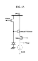
- Example FIG. 4A is an exemplary view of a driving circuit of an image sensor, in accordance with embodiments.
- Example FIG. 4B is an exemplary view of a layout of the image sensor, in accordance with embodiments.
- Example FIG. 5A is a first exemplary view of a configuration of a pixel gate driver of an image sensor, in accordance with embodiments.
- Example FIG. 5B is a second exemplary view of a configuration of a pixel gate driver of an image sensor, in accordance with embodiments.
- Example FIG. 6A is an exemplary view illustrating signal distortion in an image sensor, in accordance with embodiments.
- Example FIG. 6B is an exemplary view applying pre-emphasis in an image sensor, in accordance with embodiments.
- FIGS. 7A to 7F are cross sectional views illustrating some of a manufacturing process in an image sensor, in accordance with embodiments.
- Example FIG. 8A is a perspective view of an image sensor, in accordance with embodiments.
- Example FIG. 8B is a cross sectional view of the image sensor, in accordance with embodiments.
- Example FIG. 9 is a view illustrating sensitivity improvement in a pixel array and image sensor, in accordance with embodiments.
- Embodiments relate to a pixel array and an image sensor including the pixel array.
- a layer or film
- it can be directly on another layer or substrate, or intervening layers may also be present.
- it will be understood that when a layer is referred to as being ‘under’ another layer, it can be directly under another layer, and one or more intervening layers may also be present.
- it will also be understood that when a layer is referred to as being ‘between’ two layers, it can be the only layer between the two layers, or one or more intervening layers may also be present.
- Example FIG. 1A is a projection view of a pixel array, in accordance with embodiments.
- Example FIG. 1B is a cross sectional view of an image sensor, in accordance with embodiments.
- a pixel array (according to embodiments) may include a plurality of pixels having a pixel area P and a logic area L.
- the pixel array may include at least one of: (1) A photoelectric conversion unit 120 formed in pixel area P for each pixel. (2) A pixel-area transistor Pixel Tr disposed at a side of the photoelectric conversion unit 120 in pixel area P. (3) A metal-0 layer M 0 formed on transistor Pixel Tr. (4) A metal-1 layer M 1 formed on and/or over metal-0 layer M 0 . (5) A light reception unit 140 formed on and/or over metal-1 layer M 1 , the metal-1 layer M 1 being a top (e.g. upper-most) metal of pixel area P.
- photoelectric conversion unit 120 may be a photodiode, although but other embodiments may include other types of devices performing similar functions.
- light reception unit 140 may include a color filter 142 and/or microlens 144 , but other embodiments may include other types of devices performing similar functions.
- no metal layers may exist between metal-1 layer M 1 (e.g. as the top metal) and light reception unit 140 .
- no metal layers may exist between metal-0 layer M 0 and metal-1 layer M 1 .
- Metal-0 contact M 0 C may be disposed between metal-0 layer M 0 and substrate 110 in a pixel area.
- Metal-0 layer M 0 may electrically connect pixel-area transistors Pixel Tr of the pixels.
- through-silicon-via (TSV) 170 may be landed as wiring for metal-0 layer M 0 .
- metal-0 layer M 0 may be formed from about 500 ⁇ to about 2,000 ⁇ , the landing of the metal contact may be effectively progressed.
- metal-0 layer M 0 may not function as an etch stop layer for a through-silicon-via (TSV) in a multichip module process.
- the thickness of metal-0 layer M 0 is more than 2,000 ⁇ , capacitance may excessively increase with a decrease in a distance from the metal-1 layer. When the distance from the metal-1 layer increases to decrease the capacitance, the stack height of the image sensor may become greater.
- an image sensor of a multichip module package (PKG) type may be implemented between a chip wafer (chip/WF) having only a readout IC and a chip wafer (chip/WF) having only a pixel block.
- the metal-0 layer may be used as an etch stop layer for a through-silicon-via (TSV), thereby implementing an image sensor of a multichip module PKG type between the two chip wafer (chip/WF) after separately manufacturing the pixel block and the readout IC block, in accordance with embodiments.
- the metal-0 layer M 0 may function as a global interconnection (GIC) between transistors of pixel area P.
- GIC global interconnection
- the metal-0 layer may be used not as a local interconnection (LIC) for connecting FD nodes of small areas, but as a global interconnection (GIC) for electrically connecting pixel-area transistors of pixels, thus a pixel layout may be implemented using only up to the metal-1 layer. Accordingly, the stack height from the photodiode to microlens of a pixel may significantly decrease, thereby improving the sensitivity of the image sensor (e.g. in a small pixel).
- metal-0 layer may be formed under metal-1 layer through a tungsten damascene process used as a global interconnection (GIC).
- Logic area L may be formed at a side of pixel area P.
- transistor Logic Tr of the logic area may be formed.
- a plurality of interlayer dielectric layers 130 may be formed on the top of the transistor.
- a plurality of metals or contacts may be formed in each of the interlayer dielectric layers 130 .
- the metal of logic area L may include metal 1 M 1 , metal 2 M 2 , and/or metal 3 M 3 , although other mixes and combinations are appreciated in other embodiments.
- the contact of logic area L may include contact 1 M 1 C, contact 2, and contact 3, although other mixes and combinations are appreciated in other embodiments.
- Analog area A may be formed at another side of the pixel area P, although other arrangements are appreciated in other embodiments.
- Example FIG. 2A is an exemplary view of a driving circuit in an image sensor, in accordance with embodiments.
- Example FIG. 2B is an exemplary view of a layout of an image sensor, in accordance with embodiments.
- a pixel array may include first photodiode 120 a , second photodiode 120 b , first transfer transistor Transfer 1, second transfer transistor Transfer 2, reset transistor Reset Tr, source follower SF, and/or select transistor Select Tr.
- metal-0 layer may electrically connect pixel-area transistors of pixels.
- metal-0 layer M 0 may include at least one of the following: (1) First metal-0 layer M 01 connecting gates of the first transfer transistors Transfer 1 for the plurality of pixels. (2) Second metal-0 layer M 02 connecting gates of the select transistors Select Tr for the plurality of pixels. (3) Third metal-0 layer M 03 connecting gates of the second transfer transistors Transfer 2 for the plurality of pixels. (4) Fourth metal-0 layer M 04 connecting gates of the reset transistors Reset Tr for the plurality of pixels.
- First photodiode 120 a and second photodiode 120 b may share a floating diffusion area (FD).
- the first transfer transistor and the second transfer transistor may be electrically connected to the floating diffusion area (FD) by the metal-0 layer or metal-1 layer, although other embodiments may have different variations.
- the first metal-0 layer M 01 may be connected with the first transfer transistor Transfer 1 using a contact.
- the second metal-0 layer M 02 may be connected with the select transistor Select Tr using a contact.
- the third metal-0 layer M 03 may be connected with the second transfer transistor Transfer 2 using a contact.
- the fourth metal-0 layer M 04 may be connected with the reset transistor Reset Tr using a contact.
- the first metal-0 layer M 01 may not be connected with the select transistor Select Tr.
- the third metal-0 layer M 03 may not be connected to the reset transistor Reset Tr.
- metal-0 layer may not be used as a local interconnection (LIC), but as a global interconnection (GIC). Accordingly, the top metal of the pixel area may be formed only up to the metal-1 layer.
- the stack height from the photodiode to microlens of a pixel may be decreased significantly, which may improve the sensitivity of the image sensor, in which may be particularly important for a small pixel.
- Example FIG. 3A is an exemplary view of a driving circuit in an image sensor, in accordance with embodiments.
- Example FIG. 3B is an exemplary view of a layout of an image sensor, in accordance with embodiments.
- a pixel array and image sensor, according to embodiments, may have no select transistor and/or share 4 pixels.
- the pixel array and image sensor may include at least one of: a first transfer transistor Tx 1 , a second transfer transistor Tx 2 , a third transfer transistor Tx 3 , a fourth transfer transistor Tx 4 , a reset transistor Rx, and a drive transistor Dx, although embodiments appreciate different mixes and combinations of components.
- a metal-0 layer M 0 may electrically connect pixel-area transistors of pixels.
- metal-0 layer M 0 may include at least one of: (1) First metal-0 layer M 01 connecting gates of first transfer transistors Tx 1 for a plurality of pixels. (2) Second metal-0 layer M 02 connecting gates of second transfer transistors Tx 2 for a plurality of pixels. (3) Third metal-0 layer connecting gates of third transfer transistors Tx 3 for a plurality of pixels. (4) Fourth metal-0 layer M 04 connecting gates of fourth transfer transistors Tx 4 for a plurality of pixels. (5) Fifth metal-0 layer M 05 connecting the gates of reset transistors Rx for a plurality of pixels.
- metal-0 layer M 0 may include a sixth metal-0 layer M 06 connecting VDDs Rx VDD of the reset transistors for the plurality of pixels.
- Example FIG. 4A is an exemplary view of a driving circuit of a pixel array and image sensor, in accordance with embodiments.
- Example FIG. 4B is an exemplary view of a layout of the pixel array and image sensor, in accordance with embodiments.
- a pixel array may be a unit pixel array including three transistors 3Tr and one photodiode PD.
- the pixel array may include a reset transistor Rx, a select transistor Sx, or a drive transistor Dx, but other mixes and combinations would be appreciated in embodiments.
- Metal-0 layer M 0 may electrically connect pixel-area transistors of pixels.
- metal-0 layer M 0 may include first metal-0 layer M 01 connecting gates of the select transistors Sx for the plurality of pixels and second metal-0 layer M 02 connecting gates of the reset transistors Rx for the plurality of pixels.
- the distance between a photodiode and microlens may be significantly decreased, thereby significantly improving the sensitivity of the image sensor.
- a metal-0 layer may be used not as a local interconnection (LIC), but as a global interconnection (GIC), which may allow a pixel layout to be manufactured using only up to a metal-1 layer. Accordingly, the stack height from a photoelectric conversion unit to a light reception unit may be significantly decreased, which may significantly improve the sensitivity of the image sensor. These attributes may be particularly important for a relatively small pixel.
- Example FIG. 5A is a first exemplary view of a configuration of a pixel gate driver of an image sensor, in accordance with embodiments.
- Example FIG. 5B is a second exemplary view of a configuration of a pixel gate driver of an image sensor, in accordance with embodiments.
- Pixel gate driver 210 may be disposed at a side of a pixel array.
- Gate driver 210 may drive a transistor gate electrode of a pixel array and turn a gate on such that a voltage value for each pixel may be delivered to the pixel.
- the pixel gate driver may be disposed in parallel from right to left, which may decrease load resistance and capacitance.
- pixel gate driver 210 may include first pixel gate driver 211 disposed at one side of the pixel array and a second pixel gate driver 212 disposed at another side of the pixel array. Accordingly, dual gate drivers may be applied to decrease the load resistance and capacitance in a process, thereby driving pixels with high resolution.
- Example FIG. 6A is an exemplary view illustrating signal distortion in an image sensor.
- Example FIG. 6B is an exemplary view applying pre-emphasis in an image sensor, in accordance with embodiments.
- amplitude in frequency properties may be kept flat by applying a pre-emphasis technique which previously strengthened transmission and weakened reception, thereby driving pixels with high resolution.
- FIGS. 7A to 7F are cross sectional views illustrating some of manufacturing processes in an image sensor, in accordance with embodiments.
- first interlayer dielectric layer 131 may be formed on and/or over substrate 110
- metal-0 contact M 0 C may be formed in first interlayer dielectric layer 131 .
- Second interlayer dielectric layer 132 may be formed on and/or over metal-0 contact M 0 C, and predetermined mask pattern 310 may be formed with a photoresist.
- second interlayer dielectric layer 132 may be partially removed with reactive ion etching to form a trench T and hence expose metal-0 contact M 0 C.
- FIG. 7A first interlayer dielectric layer 131 may be formed on and/or over substrate 110
- metal-0 contact M 0 C may be formed in first interlayer dielectric layer 131 .
- Second interlayer dielectric layer 132 may be formed on and/or over metal-0 contact M 0 C, and predetermined mask pattern 310 may be formed with a photoresist.
- mask pattern 310 may be removed with ashing.
- barrier metal 161 may be formed on and/or over exposed metal-0 contact M 0 C and second interlayer dielectric layer 132 .
- metal-0 layer M 0 may be formed through a planarization process such as a CMP.
- metal-0 layer M 0 may be formed of tungsten (W), although other materials may be appreciated in accordance with embodiments.
- metal-0 layer may be used not as a local interconnection (LIC), but as a global interconnection (GIC), which may allow a pixel layout to be manufactured using only up to the metal-1 layer. Accordingly, since a pixel layout may be implemented using only up to the metal-1 layer, there may be a significant improvement to the sensitivity of the image sensor, which is particularly true for a relatively small pixel.
- a metal-0 layer may be formed under a metal-1 layer through a tungsten damascene process to be used as a global interconnection (GIC), in accordance with embodiments.
- Example FIG. 8A is a perspective view of an image sensor, in accordance with embodiments.
- Example FIG. 8B is a cross sectional view of the image sensor, in accordance with embodiments.
- a pixel chip may use similar technical features as the pixel arrays discussed above in other embodiments.
- an image sensor may be disposed under a pixel chip including a pixel array.
- the image sensor may include a readout IC (ROIC) electrically connected with the pixel array.
- a through via 170 may be formed in contact with metal-1 layer M 1 of the pixel array and electrically connected with the readout IC.
- the pixel chip and the readout IC may be combined by solder ball 190 , although substitutes for a solder ball are appreciated in accordance with embodiments.
- a multi-chip module (MCM) package may be implemented between a wafer chip (WF) where only a pixel process is progressed and a wafer chip (WF) where only a readout IC is manufactured.
- a process for removing an interlayer dielectric layer of a pixel array area e.g. trench etching
- a wafer chip process of a pixel area may be possible through processing only up to the metal-1 layer. Since a through-silicon-via landing may be possible for a wiring for the metal-0 layer, additional metal wiring may not be needed, in accordance with embodiments.
- an image sensor of a multichip module package (PKG) type may be implemented between a chip wafer (chip/WF) having only a readout IC and a chip wafer (chip/WF) having only a pixel block, in accordance with embodiments.
- a metal-0 layer may be used as an etch stop layer for a through-silicon-via TSV, thereby implementing an image sensor of a multichip module PKG type between the two chip wafer (chip/WF) after separately manufacturing the pixel block and the readout IC.
- Example FIG. 9 is a view illustrating sensitivity improvement in a pixel array and image sensor, in accordance with embodiments. According to embodiments, when a metal 1 is a top metal M 1 Top, the sensitivity improves significantly not only in an edge area but in a center area, compared with an arrangement where the metal 2 is a top metal M 2 Top.
- the distance between the photodiode and microlens may be significantly decreased, thereby significantly improving the sensitivity of the image sensor.
- the distance between a photodiode and a microlens is decreased considerably, thereby significantly improving the sensitivity of the image sensor.
- a metal-0 layer may be used not as a local interconnection (LIC), but as a global interconnection (GIC), and thus a pixel layout may be manufactured using only up to the metal-1 layer. Accordingly, the stack height from a photoelectric conversion unit to a light reception unit may be decreased significantly, thereby improving the sensitivity of the image sensor, which may be particularly true for a relatively small pixel, according to embodiments.
- a metal-0 layer may be formed under a metal-1 layer through a tungsten damascene process to be used as a global interconnection (GIC). Pixels with high resolution may be driven, adding a dual gate driver and/or pre-emphasis, according to embodiments.
- an image sensor of a multichip module package (PKG) type may be implemented between a chip wafer (chip/WF) having only a readout IC and a chip wafer (chip/WF) having only a pixel block.
- any reference in this specification to “one embodiment,” “an embodiment,” “example embodiment,” etc. means that a particular feature, structure, or characteristic described in connection with the embodiment is included in at least one embodiment of the invention.
- the appearances of such phrases in various places in the specification are not necessarily all referring to the same embodiment.
Landscapes
- Engineering & Computer Science (AREA)
- Multimedia (AREA)
- Signal Processing (AREA)
- Solid State Image Pick-Up Elements (AREA)
Abstract
Description
Claims (20)
Applications Claiming Priority (2)
| Application Number | Priority Date | Filing Date | Title |
|---|---|---|---|
| KR10-2011-0007647 | 2011-01-26 | ||
| KR1020110007647A KR101132852B1 (en) | 2011-01-26 | 2011-01-26 | Pixel array and image sensor including the same |
Publications (2)
| Publication Number | Publication Date |
|---|---|
| US20120187304A1 US20120187304A1 (en) | 2012-07-26 |
| US8895936B2 true US8895936B2 (en) | 2014-11-25 |
Family
ID=46143188
Family Applications (1)
| Application Number | Title | Priority Date | Filing Date |
|---|---|---|---|
| US13/342,437 Active 2032-09-24 US8895936B2 (en) | 2011-01-26 | 2012-01-03 | Pixel array and image sensor including the same |
Country Status (2)
| Country | Link |
|---|---|
| US (1) | US8895936B2 (en) |
| KR (1) | KR101132852B1 (en) |
Families Citing this family (6)
| Publication number | Priority date | Publication date | Assignee | Title |
|---|---|---|---|---|
| CN102833497B (en) | 2012-08-03 | 2014-11-19 | 昆山锐芯微电子有限公司 | Image sensor and image processing system |
| US9343497B2 (en) | 2012-09-20 | 2016-05-17 | Semiconductor Components Industries, Llc | Imagers with stacked integrated circuit dies |
| JP6445978B2 (en) | 2012-12-03 | 2018-12-26 | コーニンクレッカ フィリップス エヌ ヴェKoninklijke Philips N.V. | Imaging detector |
| KR102197026B1 (en) | 2014-02-25 | 2020-12-31 | 삼성디스플레이 주식회사 | Organic light emitting display device |
| KR102617430B1 (en) * | 2016-11-08 | 2023-12-26 | 에스케이하이닉스 주식회사 | Image sensor |
| CN113903754A (en) * | 2020-07-06 | 2022-01-07 | 思特威(上海)电子科技股份有限公司 | CMOS image sensor and manufacturing method thereof |
Citations (9)
| Publication number | Priority date | Publication date | Assignee | Title |
|---|---|---|---|---|
| JP2001337170A (en) | 2001-03-23 | 2001-12-07 | Toshiba Corp | X-ray imaging apparatus and X-ray detection apparatus |
| US20040217396A1 (en) * | 2003-04-30 | 2004-11-04 | Won-Ho Lee | Unit pixel in CMOS image sensor |
| US20080186724A1 (en) * | 2001-01-23 | 2008-08-07 | Donnelly Corporation | Video mirror system for a vehicle |
| JP2010074631A (en) * | 2008-09-19 | 2010-04-02 | Canon Inc | Solid-state image pickup apparatus and image pickup system |
| US20100116999A1 (en) * | 2004-03-26 | 2010-05-13 | Nova R&D, Inc. | High Resolution Imaging System |
| KR20100073786A (en) | 2008-12-23 | 2010-07-01 | 주식회사 동부하이텍 | Image sensor and method for manufacturing thereof |
| KR20100077564A (en) | 2008-12-29 | 2010-07-08 | 주식회사 동부하이텍 | Image sensor and method for manufacturing thereof |
| US20100245637A1 (en) * | 2009-03-31 | 2010-09-30 | Sony Corporation | Solid-state imaging device, method of manufacturing the same, and electronic apparatus |
| US7863936B1 (en) * | 2009-12-01 | 2011-01-04 | Himax Imaging, Inc. | Driving circuit with impedence calibration and pre-emphasis functionalities |
-
2011
- 2011-01-26 KR KR1020110007647A patent/KR101132852B1/en active Active
-
2012
- 2012-01-03 US US13/342,437 patent/US8895936B2/en active Active
Patent Citations (9)
| Publication number | Priority date | Publication date | Assignee | Title |
|---|---|---|---|---|
| US20080186724A1 (en) * | 2001-01-23 | 2008-08-07 | Donnelly Corporation | Video mirror system for a vehicle |
| JP2001337170A (en) | 2001-03-23 | 2001-12-07 | Toshiba Corp | X-ray imaging apparatus and X-ray detection apparatus |
| US20040217396A1 (en) * | 2003-04-30 | 2004-11-04 | Won-Ho Lee | Unit pixel in CMOS image sensor |
| US20100116999A1 (en) * | 2004-03-26 | 2010-05-13 | Nova R&D, Inc. | High Resolution Imaging System |
| JP2010074631A (en) * | 2008-09-19 | 2010-04-02 | Canon Inc | Solid-state image pickup apparatus and image pickup system |
| KR20100073786A (en) | 2008-12-23 | 2010-07-01 | 주식회사 동부하이텍 | Image sensor and method for manufacturing thereof |
| KR20100077564A (en) | 2008-12-29 | 2010-07-08 | 주식회사 동부하이텍 | Image sensor and method for manufacturing thereof |
| US20100245637A1 (en) * | 2009-03-31 | 2010-09-30 | Sony Corporation | Solid-state imaging device, method of manufacturing the same, and electronic apparatus |
| US7863936B1 (en) * | 2009-12-01 | 2011-01-04 | Himax Imaging, Inc. | Driving circuit with impedence calibration and pre-emphasis functionalities |
Also Published As
| Publication number | Publication date |
|---|---|
| US20120187304A1 (en) | 2012-07-26 |
| KR101132852B1 (en) | 2012-04-03 |
Similar Documents
| Publication | Publication Date | Title |
|---|---|---|
| US12419129B2 (en) | Semiconductor device and method of manufacturing the same, and electronic apparatus | |
| US10096645B2 (en) | Method and apparatus for image sensor packaging | |
| US9917123B2 (en) | Method and apparatus for image sensor packaging | |
| JP5843475B2 (en) | Solid-state imaging device and method for manufacturing solid-state imaging device | |
| US10367022B2 (en) | Solid-state imaging device, members for the same, and imaging system | |
| US10090349B2 (en) | CMOS image sensor chips with stacked scheme and methods for forming the same | |
| US8895936B2 (en) | Pixel array and image sensor including the same | |
| US20150263063A1 (en) | Integrated circuit process | |
| CN206480627U (en) | Imaging sensor and image sensor IC | |
| JP2019195082A (en) | Solid-state imaging device and method for manufacturing solid-state imaging device | |
| CN112397536A (en) | Image sensor with a plurality of pixels | |
| CN107425026A (en) | Semiconductor devices and its manufacture method |
Legal Events
| Date | Code | Title | Description |
|---|---|---|---|
| AS | Assignment |
Owner name: DONGBU HITEK CO., LTD., KOREA, REPUBLIC OF Free format text: ASSIGNMENT OF ASSIGNORS INTEREST;ASSIGNORS:HA, MAN LYUN;LEE, JU IL;CHOI, SUN;SIGNING DATES FROM 20111216 TO 20111217;REEL/FRAME:027469/0891 |
|
| STCF | Information on status: patent grant |
Free format text: PATENTED CASE |
|
| AS | Assignment |
Owner name: DB HITEK CO., LTD., KOREA, REPUBLIC OF Free format text: CHANGE OF NAME;ASSIGNOR:DONGBU HITEK CO., LTD.;REEL/FRAME:044559/0819 Effective date: 20171101 |
|
| MAFP | Maintenance fee payment |
Free format text: PAYMENT OF MAINTENANCE FEE, 4TH YEAR, LARGE ENTITY (ORIGINAL EVENT CODE: M1551) Year of fee payment: 4 |
|
| MAFP | Maintenance fee payment |
Free format text: PAYMENT OF MAINTENANCE FEE, 8TH YEAR, LARGE ENTITY (ORIGINAL EVENT CODE: M1552); ENTITY STATUS OF PATENT OWNER: LARGE ENTITY Year of fee payment: 8 |