US8885679B1 - Mode-hop free athermal laser - Google Patents
Mode-hop free athermal laser Download PDFInfo
- Publication number
- US8885679B1 US8885679B1 US13/907,569 US201313907569A US8885679B1 US 8885679 B1 US8885679 B1 US 8885679B1 US 201313907569 A US201313907569 A US 201313907569A US 8885679 B1 US8885679 B1 US 8885679B1
- Authority
- US
- United States
- Prior art keywords
- laser
- optical
- phase
- optical signal
- phase shifting
- Prior art date
- Legal status (The legal status is an assumption and is not a legal conclusion. Google has not performed a legal analysis and makes no representation as to the accuracy of the status listed.)
- Active
Links
Images


Classifications
-
- H—ELECTRICITY
- H01—ELECTRIC ELEMENTS
- H01S—DEVICES USING THE PROCESS OF LIGHT AMPLIFICATION BY STIMULATED EMISSION OF RADIATION [LASER] TO AMPLIFY OR GENERATE LIGHT; DEVICES USING STIMULATED EMISSION OF ELECTROMAGNETIC RADIATION IN WAVE RANGES OTHER THAN OPTICAL
- H01S5/00—Semiconductor lasers
- H01S5/06—Arrangements for controlling the laser output parameters, e.g. by operating on the active medium
- H01S5/062—Arrangements for controlling the laser output parameters, e.g. by operating on the active medium by varying the potential of the electrodes
- H01S5/0625—Arrangements for controlling the laser output parameters, e.g. by operating on the active medium by varying the potential of the electrodes in multi-section lasers
- H01S5/06255—Controlling the frequency of the radiation
- H01S5/06256—Controlling the frequency of the radiation with DBR-structure
-
- H—ELECTRICITY
- H01—ELECTRIC ELEMENTS
- H01S—DEVICES USING THE PROCESS OF LIGHT AMPLIFICATION BY STIMULATED EMISSION OF RADIATION [LASER] TO AMPLIFY OR GENERATE LIGHT; DEVICES USING STIMULATED EMISSION OF ELECTROMAGNETIC RADIATION IN WAVE RANGES OTHER THAN OPTICAL
- H01S5/00—Semiconductor lasers
- H01S5/06—Arrangements for controlling the laser output parameters, e.g. by operating on the active medium
- H01S5/068—Stabilisation of laser output parameters
-
- H—ELECTRICITY
- H01—ELECTRIC ELEMENTS
- H01S—DEVICES USING THE PROCESS OF LIGHT AMPLIFICATION BY STIMULATED EMISSION OF RADIATION [LASER] TO AMPLIFY OR GENERATE LIGHT; DEVICES USING STIMULATED EMISSION OF ELECTROMAGNETIC RADIATION IN WAVE RANGES OTHER THAN OPTICAL
- H01S5/00—Semiconductor lasers
- H01S5/06—Arrangements for controlling the laser output parameters, e.g. by operating on the active medium
- H01S5/062—Arrangements for controlling the laser output parameters, e.g. by operating on the active medium by varying the potential of the electrodes
- H01S5/06233—Controlling other output parameters than intensity or frequency
- H01S5/06246—Controlling other output parameters than intensity or frequency controlling the phase
-
- H—ELECTRICITY
- H01—ELECTRIC ELEMENTS
- H01S—DEVICES USING THE PROCESS OF LIGHT AMPLIFICATION BY STIMULATED EMISSION OF RADIATION [LASER] TO AMPLIFY OR GENERATE LIGHT; DEVICES USING STIMULATED EMISSION OF ELECTROMAGNETIC RADIATION IN WAVE RANGES OTHER THAN OPTICAL
- H01S5/00—Semiconductor lasers
- H01S5/06—Arrangements for controlling the laser output parameters, e.g. by operating on the active medium
- H01S5/068—Stabilisation of laser output parameters
- H01S5/0683—Stabilisation of laser output parameters by monitoring the optical output parameters
- H01S5/0687—Stabilising the frequency of the laser
-
- H—ELECTRICITY
- H01—ELECTRIC ELEMENTS
- H01S—DEVICES USING THE PROCESS OF LIGHT AMPLIFICATION BY STIMULATED EMISSION OF RADIATION [LASER] TO AMPLIFY OR GENERATE LIGHT; DEVICES USING STIMULATED EMISSION OF ELECTROMAGNETIC RADIATION IN WAVE RANGES OTHER THAN OPTICAL
- H01S5/00—Semiconductor lasers
- H01S5/10—Construction or shape of the optical resonator, e.g. extended or external cavity, coupled cavities, bent-guide, varying width, thickness or composition of the active region
- H01S5/14—External cavity lasers
- H01S5/141—External cavity lasers using a wavelength selective device, e.g. a grating or etalon
-
- H—ELECTRICITY
- H01—ELECTRIC ELEMENTS
- H01S—DEVICES USING THE PROCESS OF LIGHT AMPLIFICATION BY STIMULATED EMISSION OF RADIATION [LASER] TO AMPLIFY OR GENERATE LIGHT; DEVICES USING STIMULATED EMISSION OF ELECTROMAGNETIC RADIATION IN WAVE RANGES OTHER THAN OPTICAL
- H01S3/00—Lasers, i.e. devices using stimulated emission of electromagnetic radiation in the infrared, visible or ultraviolet wave range
- H01S3/05—Construction or shape of optical resonators; Accommodation of active medium therein; Shape of active medium
- H01S3/08—Construction or shape of optical resonators or components thereof
- H01S3/08059—Constructional details of the reflector, e.g. shape
-
- H—ELECTRICITY
- H01—ELECTRIC ELEMENTS
- H01S—DEVICES USING THE PROCESS OF LIGHT AMPLIFICATION BY STIMULATED EMISSION OF RADIATION [LASER] TO AMPLIFY OR GENERATE LIGHT; DEVICES USING STIMULATED EMISSION OF ELECTROMAGNETIC RADIATION IN WAVE RANGES OTHER THAN OPTICAL
- H01S5/00—Semiconductor lasers
- H01S5/10—Construction or shape of the optical resonator, e.g. extended or external cavity, coupled cavities, bent-guide, varying width, thickness or composition of the active region
- H01S5/1003—Waveguide having a modified shape along the axis, e.g. branched, curved, tapered, voids
- H01S5/1007—Branched waveguides
Definitions
- Embodiments of the invention generally pertain to optical devices and more specifically to athermal laser cavities.
- the output characteristics of a semiconductor laser depend, in part, on its operating temperature.
- the wavelength of a laser's output signal may change gradually with temperature; however, at some temperature values, the wavelength of the laser's output signal may make discrete jumps.
- FIG. 1 is a graph illustrating an example of these discrete jumps as a function of device temperature. As illustrated in graph 100 , these jumps occur when device temperature increases and the output signal changes from one longitudinal mode to another (referred to herein as “mode-hopping”).
- FIG. 1 is a graph illustrating “mode-hopping” in prior art laser devices.
- FIG. 2 is an illustration of mode-hop free lasers according to embodiments of the invention.
- FIG. 3 is an illustration of a retroreflective endless phase shifter to eliminate mode-hops according to an embodiment of the invention.
- FIG. 4 is a flow diagram for adjusting the round-trip phase of the optical path in a laser cavity at the operating wavelength to eliminate mode-hops according to an embodiment of the invention.
- FIG. 5 is an illustration of a mode-hop free tunable laser according to an embodiment of the invention.
- Embodiments of the invention describe systems, apparatuses and methods for eliminating mode-hops in the presence of laser device temperature fluctuations (e.g., temperature changes in the laser cavity).
- laser device temperature fluctuations e.g., temperature changes in the laser cavity.
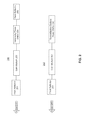
- FIG. 2 is an illustration of mode-hop free lasers according to embodiments of the invention.
- Laser 200 is shown to include a laser cavity formed by front reflector 201 and back reflector 202 ; gain medium 203 and intracavity phase shifter 204 are included in said laser cavity. While illustrated in this example as a linear cavity, said laser cavity may comprise any shape in other embodiments of the invention; for example, in some embodiments, ring-shaped laser cavities are utilized.
- An optical signal is transmitted from laser 200 via output port 210 .
- Gain medium 203 may comprise any structure or material suitable for amplifying an optical signal.
- gain medium 203 may be formed from a III-V semiconductor material, a germanium (Ge) material, etc.
- the components of laser 200 may be formed from any combination of suitable semiconductor materials—e.g., formed from both a silicon and a non-silicon material.
- Said non-silicon material (alternatively referred to as “heterogeneous material”) may comprise one of III-V material, magneto-optic material, or crystal substrate material.
- Laser 200 may further be included in a system of discrete optical components, or in a photonic integrated circuit (PIC) comprising multiple optical components.
- PIC photonic integrated circuit
- phase shifting component such as intracavity phase shifter 204
- phase shifter 204 may utilize any suitable process for changing the phase of the optical signal of laser 200 , such as utilizing resistive heaters, resistive heating of doped silicon, silicon carrier injection or depletion modulators, heterogeneous-integrated III-V phase modulators, or native substrate III-V phase modulators.
- phase shifter 204 is used to form a configurable optical cavity length for laser 200 .
- Embodiments of the invention thus utilize a plurality of optical cavity lengths including one or more optical cavity lengths to potentially shift the phase of the optical signal to maintain a laser cavity's output wavelength and avoid mode-hops in the presence of fluctuations such as temperature drift or laser drive current changes (detected via any feedback component suitable to detect a phase/frequency/wavelength change of the optical signal of laser 200 ).
- a switch may be included in said optical cavity to select an optical cavity length for the optical signal: a first optical cavity length and a second configurable cavity length.
- said first optical cavity length comprises a ‘constant’ (i.e., fixed) length; in other embodiments, however, said first optical cavity length may also be configurable.
- said switch may comprise a Mach-Zehnder Interferometer (MZI).
- MZI Mach-Zehnder Interferometer
- the switch may select a second optical cavity length configurable to shift the phase of the optical signal, the second optical cavity length formed from a plurality of optical couplers (for example, multimode interference (MMI) structures and directional couplers).
- the second (configurable) optical cavity length comprises the same effective length as the first (constant) optical cavity length when the phase is shifted by an integer multiple of 2*PI.
- the phase shifting component is adjusted to avoid mode hops by compensating for phase shifts caused by temperature fluctuations in the rest of the laser cavity.
- the total required phase shift range may be quite large (i.e., many cycles of 2*PI), especially in embodiments comprising long-cavity lasers operated over a large temperature range, due to the dn/dT of the material making up the cavity.
- the phase shifting component may be able to continuously shift the phase without limit (alternatively referred to herein as an “endless phase shifter”).
- Embodiments of the invention allow for the continuous shifting of phase at a single frequency without a discontinuity—e.g., utilize a single phase shifting component with a range of at least 0-2*PI (e.g., 0-4*PI, etc.).
- Laser 250 of FIG. 2 illustrates an alternative architecture for an athermal laser cavity utilizing a retroreflective phase shifter.
- Laser 250 is shown to include a cavity formed from front reflector 251 and retroreflective phase shifter 252 ; gain medium 253 amplifies the optical signal, which is subsequently output via output port 260 .
- An example architecture of retroreflective phase shifter 252 is discussed below.
- FIG. 3 is an illustration of a retroreflective endless phase shifter to eliminate mode-hops according to an embodiment of the invention.
- endless phase shifter 300 includes phase shifting components 304 and 308 , and a plurality of couplers to selectively direct an optical signal to retroreflective optical paths 360 (including phase shifting component 308 ) or 362 (i.e., 1 ⁇ 2 couplers 302 , 310 and 312 and 2 ⁇ 2 coupler 306 ).
- these couplers may be MMIs or directional couplers.
- Couplers 302 and 306 , waveguides 350 and 352 , and phase shifting component 304 comprise an MZI designed to switch the light from input/output port 301 to either of the retroreflective paths, either upper path 360 including phase shifter 308 , 1 ⁇ 2 coupler 310 , and ring 314 , or lower path 362 including 1 ⁇ 2 coupler 312 and ring 316 .
- Phase shifting component 304 may therefore switch between discrete phase shift values and phase shifter 308 may tune smoothly except during a ‘reset’ switching operation (i.e., resetting the phase shifter away from its minimum or maximum phase shifting limit).
- Phase shifting component 308 may comprise any range such that the phase difference between retroreflective optical paths 360 and 362 comprises an integer multiple of 2*PI (and thus induce the same return phase); in other words, for a laser cavity utilizing endless phase shifter 300 in the configuration shown in FIG. 2 to be mode-hop-free at a particular output wavelength, the absolute optical path length does not need to remain constant but the net phase shift in a round trip of the cavity is an integer multiple of 2*PI.
- component 304 may comprise a line phase shifter having a range of PI/2-3*PI/2
- component 308 may comprise a line phase shifter having a range of 0-2*PI.
- phase shifting components and couplers are included in the cavity of endless phase shifter 300 , and further utilize the retroreflector of the laser (as shown by retroreflective loops 314 and 316 ) so that the light passes twice through phase shifting component 308 , thereby reducing the amount of phase shift and switching needed in this embodiment.
- phase-shifting range In contrast to prior art solutions utilizing a heater-based phase shifter to compensate over a large temperature range employing a wide range of phase shift, use of this invention allows the phase-shifting range to be limited to a smaller range (e.g., 2*PI radians, 4*PI radians).
- a reset function is employed where the light is switched from path 360 containing the phase shifter to path 362 (which comprises a constant optical cavity length), and the phase shifter is shifted by 2*PI towards the center of its range.
- the optical signal of endless phase shifter 300 is switched from phase shifter path 360 to alternate path 362 , resets phase shifter component 308 towards the center of its range, and the optical signal of endless phase shifter 300 is switched back to phase shifter path 360 when its net phase is an integer multiple 2*PI of the phase of path 362 .
- the above described process ensures that no mode-hops are present during the transition and the optical signal output remains stable.
- An example process for operating a mode-hop free laser is discussed below.
- FIG. 4 is a flow diagram for adjusting the round-trip phase of the optical path in a laser cavity at the operating wavelength to eliminate mode-hops according to an embodiment of the invention.
- Flow diagrams as illustrated herein provide examples of sequences of various process actions. Although shown in a particular sequence or order, unless otherwise specified, the order of the actions can be modified. Thus, the illustrated implementations should be understood only as examples, and the illustrated processes can be performed in a different order, and some actions may be performed in parallel. Additionally, one or more actions can be omitted in various embodiments of the disclosure; thus, not all actions are required in every implementation. Other process flows are possible.
- Process 400 includes operations for identifying a phase status of an optical signal in a laser cavity of a laser, 402 ; said optical signal goes through a path having a configurable optical cavity length (rather than an alternative path such as a ‘fixed’ path having a fixed optical cavity length or another configurable optical path), where it is continuously measured to detect any phase change.
- Said optical signal is either in phase, or is changing phase due to the presence of operating condition fluctuations such as temperature drift or changes to the laser's drive current. This change in phase is indicative of a potential mode-hop, as described above.
- phase shift in the configurable optical cavity length i.e., path
- the phase shift in the configurable optical cavity length is adjusted so that the phase change is re-adjusted to zero (i.e., a feedback loop).
- a maximum or minimum (max/min) value in the phase shifter's range it is determined if a maximum or minimum (max/min) value in the phase shifter's range has been reached, 406 . If the configurable optical cavity length is at the max/min of its phase range, then a ‘reset’ process is initiated.
- the two optical cavity lengths (i.e., the configurable and fixed path length) differ by zero or by n*2*PI.
- Light is switched from the configurable to the fixed path, 410 .
- the configurable phase shifter is reset closer to or at the center of its operating range, where the fixed and configurable paths still differ by n*2*PI, 412 .
- Light is then switched from the fixed to the configurable path, 414 .
- the process returns to feedback/tracking operations (i.e., back to operation 402 ) so that configurable phase may be shifted to compensate for cavity changes (until it hits the max/min condition again).
- FIG. 5 is an illustration of a mode-hop free tunable laser according to an embodiment of the invention.
- laser 500 includes retroreflective output/filtering component 502 , gain medium 504 and retroreflective phase shifter 506 .
- Retroreflective output/filtering component 502 may comprise a plurality of ring filters forming a Vernier filter—e.g., a plurality of ring filters with varying radii for tuning the output signal due to the Vernier effect (i.e., a large tuning effect is accomplished by exploiting the Vernier effect, by which small relative refractive index changes may be used to yield large relative wavelength changes. Additionally by using a pair of filter elements the combined Vernier filter can have a larger free spectral range, thus filtering out unintended modes over a larger wavelength range than a single filter element).
- this embodiment describes a mode-hop free tunable laser wherein the functionality for output signal tuning and stabilization are included in a laser cavity.
- the above described embodiments of the invention may comprise silicon-on-insulator (SOI) or silicon based (e.g., silicon nitride (SiN)) devices, or may comprise devices formed from both silicon and a non-silicon material.
- Said non-silicon material (alternatively referred to as “heterogeneous material”) may comprise one of III-V material, magneto-optic material, or crystal substrate material.
- III-V semiconductors have elements that are found in group III and group V of the periodic table (e.g., Indium Gallium Arsenide Phosphide (InGaAsP), Gallium Indium Arsenide Nitride (GaInAsN)).
- the carrier dispersion effects of III-V based materials may be significantly higher than in silicon based materials, as electron speed in III-V semiconductors is much faster than that in silicon.
- III-V materials have a direct bandgap which enables efficient creation of light from electrical pumping.
- III-V semiconductor materials enable photonic operations with an increased efficiency over silicon for both generating light and modulating the refractive index of light.
- III-V semiconductor materials enable photonic operation with an increased efficiency at generating light from electricity and converting light back into electricity.
- the low optical loss and high quality oxides of silicon are thus combined with the electro-optic efficiency of III-V semiconductors in the heterogeneous optical devices described below; in embodiments of the invention, said heterogeneous devices utilize low loss heterogeneous optical waveguide transitions between the devices' heterogeneous and silicon-only waveguides.
- Magneto-optic materials allow heterogeneous PICs to operate based on the magneto-optic (MO) effect.
- Such devices may devices utilize the Faraday Effect, in which the magnetic field associated with an electrical signal modulates an optical beam, offering high bandwidth modulation, and rotates the electric field of the optical mode enabling optical isolators.
- Said magneto-optic materials may comprise, for example, materials such as such as iron, cobalt, or yttrium iron garnet (YIG).
- Crystal substrate materials provide heterogeneous PICs with a high electro-mechanical coupling linear electro optic coefficient, low transmission loss, and stable physical and chemical properties.
- Said crystal substrate materials may comprise, for example, lithium niobate (LiNbO3) or lithium tantalate (LiTaO3).
Landscapes
- Physics & Mathematics (AREA)
- Condensed Matter Physics & Semiconductors (AREA)
- General Physics & Mathematics (AREA)
- Electromagnetism (AREA)
- Optics & Photonics (AREA)
- Optical Modulation, Optical Deflection, Nonlinear Optics, Optical Demodulation, Optical Logic Elements (AREA)
Abstract
Description
Claims (20)
Priority Applications (1)
| Application Number | Priority Date | Filing Date | Title |
|---|---|---|---|
| US13/907,569 US8885679B1 (en) | 2013-05-31 | 2013-05-31 | Mode-hop free athermal laser |
Applications Claiming Priority (1)
| Application Number | Priority Date | Filing Date | Title |
|---|---|---|---|
| US13/907,569 US8885679B1 (en) | 2013-05-31 | 2013-05-31 | Mode-hop free athermal laser |
Publications (1)
| Publication Number | Publication Date |
|---|---|
| US8885679B1 true US8885679B1 (en) | 2014-11-11 |
Family
ID=51845834
Family Applications (1)
| Application Number | Title | Priority Date | Filing Date |
|---|---|---|---|
| US13/907,569 Active US8885679B1 (en) | 2013-05-31 | 2013-05-31 | Mode-hop free athermal laser |
Country Status (1)
| Country | Link |
|---|---|
| US (1) | US8885679B1 (en) |
Cited By (9)
| Publication number | Priority date | Publication date | Assignee | Title |
|---|---|---|---|---|
| US10468854B1 (en) * | 2013-06-28 | 2019-11-05 | Aurrion, Inc. | Polarization insensitive colorless optical devices |
| US20190368859A1 (en) * | 2013-06-23 | 2019-12-05 | Eric Swanson | Wavelength Tunable Laser Device |
| US10641964B2 (en) | 2018-03-22 | 2020-05-05 | Keysight Technologies, Inc. | Continuous phase tuning system with loop mirror |
| US10840672B2 (en) | 2017-08-18 | 2020-11-17 | Nokia Solutions And Networks Oy | Mode-locked semiconductor laser capable of changing output-comb frequency spacing |
| US20210126421A1 (en) * | 2019-10-24 | 2021-04-29 | Fujitsu Limited | Wavelength tunable light source, optical transmission apparatus using the same, and method of controlling wavelength tunable light source |
| US11044018B1 (en) * | 2018-07-23 | 2021-06-22 | Source Photonics, Inc. | Optical modulator and methods of making and using the same |
| US11579356B2 (en) | 2013-06-23 | 2023-02-14 | Eric Swanson | Integrated optical system with wavelength tuning and spatial switching |
| CN117895322A (en) * | 2024-03-18 | 2024-04-16 | 北京弘光向尚科技有限公司 | Method for reducing mode-jump phenomenon of external cavity tunable laser |
| US12085387B1 (en) | 2023-09-23 | 2024-09-10 | Hamamatsu Photonics K.K. | Optical coherence tomography system for subsurface inspection |
Citations (7)
| Publication number | Priority date | Publication date | Assignee | Title |
|---|---|---|---|---|
| US3487327A (en) * | 1967-11-01 | 1969-12-30 | Hughes Aircraft Co | Frequency stabilized laser |
| US5022034A (en) * | 1989-06-27 | 1991-06-04 | May A D | Laser device, including control of polarization mode |
| US5313333A (en) | 1992-12-23 | 1994-05-17 | Estman Kodak Company | Method and apparatus for combined active and passive athermalization of an optical assembly |
| US5914972A (en) | 1997-03-24 | 1999-06-22 | Sdl, Inc. | Thermal compensators for waveguide DBR laser sources |
| US6320888B1 (en) | 1997-09-19 | 2001-11-20 | Nippon Telegraph & Telephone Corporation | Frequency stabilized laser and method for preparing thereof |
| US20130044974A1 (en) | 2011-08-15 | 2013-02-21 | Alcatel-Lucent Usa Inc. | Endless phase shifting |
| US8594144B1 (en) * | 2009-05-07 | 2013-11-26 | L-3 Insight Technology Incorporated | Pump diode driver circuit |
-
2013
- 2013-05-31 US US13/907,569 patent/US8885679B1/en active Active
Patent Citations (7)
| Publication number | Priority date | Publication date | Assignee | Title |
|---|---|---|---|---|
| US3487327A (en) * | 1967-11-01 | 1969-12-30 | Hughes Aircraft Co | Frequency stabilized laser |
| US5022034A (en) * | 1989-06-27 | 1991-06-04 | May A D | Laser device, including control of polarization mode |
| US5313333A (en) | 1992-12-23 | 1994-05-17 | Estman Kodak Company | Method and apparatus for combined active and passive athermalization of an optical assembly |
| US5914972A (en) | 1997-03-24 | 1999-06-22 | Sdl, Inc. | Thermal compensators for waveguide DBR laser sources |
| US6320888B1 (en) | 1997-09-19 | 2001-11-20 | Nippon Telegraph & Telephone Corporation | Frequency stabilized laser and method for preparing thereof |
| US8594144B1 (en) * | 2009-05-07 | 2013-11-26 | L-3 Insight Technology Incorporated | Pump diode driver circuit |
| US20130044974A1 (en) | 2011-08-15 | 2013-02-21 | Alcatel-Lucent Usa Inc. | Endless phase shifting |
Non-Patent Citations (3)
| Title |
|---|
| Doerr, Christopher R., "Proposed Architecture for MIMO Optical Demultiplexing Using Photonic Integration, IEEE Photonics Technology Letters", vol. 23, No. 21, Nov. 1, 2011, 1573-1575. |
| Phelan, R., et al., "2408C < T < 958 C mode-hop-free operation of uncooled AIGaInAs-MQW discrete-mode laser diode with emission at lambda = 1.3 mum", Electronics Letters, Jan. 1, 2009, vol. 45 No. 1, (Jan. 1, 2009), pp. 2. |
| Phelan, R., et al., "2408C < T < 958 C mode-hop-free operation of uncooled AIGaInAs-MQW discrete-mode laser diode with emission at λ = 1.3 μm", Electronics Letters, Jan. 1, 2009, vol. 45 No. 1, (Jan. 1, 2009), pp. 2. |
Cited By (14)
| Publication number | Priority date | Publication date | Assignee | Title |
|---|---|---|---|---|
| US10876827B2 (en) * | 2013-06-23 | 2020-12-29 | Eric Swanson | Multi-cavity wavelength tunable laser device |
| US20190368859A1 (en) * | 2013-06-23 | 2019-12-05 | Eric Swanson | Wavelength Tunable Laser Device |
| US11579356B2 (en) | 2013-06-23 | 2023-02-14 | Eric Swanson | Integrated optical system with wavelength tuning and spatial switching |
| US11397075B2 (en) | 2013-06-23 | 2022-07-26 | Eric Swanson | Photonic integrated receiver |
| US11437786B2 (en) | 2013-06-28 | 2022-09-06 | Openlight Photonics, Inc. | Polarization insensitive colorless optical devices |
| US10756516B2 (en) | 2013-06-28 | 2020-08-25 | Aurrion, Inc. | Polarization insensitive colorless optical devices |
| US10468854B1 (en) * | 2013-06-28 | 2019-11-05 | Aurrion, Inc. | Polarization insensitive colorless optical devices |
| US10840672B2 (en) | 2017-08-18 | 2020-11-17 | Nokia Solutions And Networks Oy | Mode-locked semiconductor laser capable of changing output-comb frequency spacing |
| US10641964B2 (en) | 2018-03-22 | 2020-05-05 | Keysight Technologies, Inc. | Continuous phase tuning system with loop mirror |
| US11044018B1 (en) * | 2018-07-23 | 2021-06-22 | Source Photonics, Inc. | Optical modulator and methods of making and using the same |
| US20210126421A1 (en) * | 2019-10-24 | 2021-04-29 | Fujitsu Limited | Wavelength tunable light source, optical transmission apparatus using the same, and method of controlling wavelength tunable light source |
| US11664644B2 (en) * | 2019-10-24 | 2023-05-30 | Fujitsu Limited | Wavelength tunable light source, optical transmission apparatus using the same, and method of controlling wavelength tunable light source |
| US12085387B1 (en) | 2023-09-23 | 2024-09-10 | Hamamatsu Photonics K.K. | Optical coherence tomography system for subsurface inspection |
| CN117895322A (en) * | 2024-03-18 | 2024-04-16 | 北京弘光向尚科技有限公司 | Method for reducing mode-jump phenomenon of external cavity tunable laser |
Similar Documents
| Publication | Publication Date | Title |
|---|---|---|
| US8885679B1 (en) | Mode-hop free athermal laser | |
| US9979489B2 (en) | Optical modulation apparatus, optical transmitter and controlling method for optical modulator | |
| EP2575220B1 (en) | Tunable laser with integrated wavelength reference | |
| US10281746B2 (en) | Wavelength-tunable III-V/Si hybrid optical transmitter | |
| US9318868B2 (en) | Tunable hybrid laser with carrier-induced phase control | |
| US8559470B2 (en) | Method and system for hybrid integration of a tunable laser and a phase modulator | |
| US8867578B2 (en) | Method and system for hybrid integration of a tunable laser for a cable TV transmitter | |
| JP5315792B2 (en) | Light modulator | |
| US10236657B2 (en) | Device and method for tuning a ring resonator using self-heating stabilization | |
| US9509114B1 (en) | Multi-wavelength laser cavity | |
| US10211595B2 (en) | Densely arrayed waveguides with low cross-coupling | |
| US9136666B1 (en) | Mode-hop tolerant semiconductor laser design | |
| US10090632B2 (en) | Lasing output based on varying modal index | |
| EP2871504A1 (en) | Optical mode steering for wavelength stabilization | |
| US20240348006A1 (en) | Silicon photonic symmetric distributed feedback laser | |
| US9529153B2 (en) | Optical apparatus including nested resonator | |
| Romero-García et al. | Broadband, temperature tolerant and passively biased resonantly enhanced Mach-Zehnder modulators | |
| US20130156061A1 (en) | Arrangement for Generating Fast Wavelength-Switched Optical Signal | |
| Melikyan et al. | Wavelength stabilized silicon/III-V hybrid laser | |
| Saeedi et al. | Differential optical ring modulator: Breaking the bandwidth/quality-factor trade-off | |
| Hinokuma et al. | Single-wavelength emission by using 1× N active multi-mode interferometer laser diode | |
| AlTaha et al. | Silicon-photonic devices: Electronic control and stabilization | |
| Zhou et al. | Integrated tunable silicon photonic devices for optical filter and delay applications |
Legal Events
| Date | Code | Title | Description |
|---|---|---|---|
| AS | Assignment |
Owner name: AURRION, INC., CALIFORNIA Free format text: ASSIGNMENT OF ASSIGNORS INTEREST;ASSIGNORS:ROTH, JONATHAN EDGAR;FISH, GREGORY ALAN;NORBERG, ERIK JOHAN;AND OTHERS;SIGNING DATES FROM 20130523 TO 20130531;REEL/FRAME:030527/0822 |
|
| FEPP | Fee payment procedure |
Free format text: PAYOR NUMBER ASSIGNED (ORIGINAL EVENT CODE: ASPN); ENTITY STATUS OF PATENT OWNER: LARGE ENTITY |
|
| STCF | Information on status: patent grant |
Free format text: PATENTED CASE |
|
| FEPP | Fee payment procedure |
Free format text: PAT HOLDER NO LONGER CLAIMS SMALL ENTITY STATUS, ENTITY STATUS SET TO UNDISCOUNTED (ORIGINAL EVENT CODE: STOL); ENTITY STATUS OF PATENT OWNER: LARGE ENTITY |
|
| MAFP | Maintenance fee payment |
Free format text: PAYMENT OF MAINTENANCE FEE, 4TH YEAR, LARGE ENTITY (ORIGINAL EVENT CODE: M1551) Year of fee payment: 4 |
|
| MAFP | Maintenance fee payment |
Free format text: PAYMENT OF MAINTENANCE FEE, 8TH YEAR, LARGE ENTITY (ORIGINAL EVENT CODE: M1552); ENTITY STATUS OF PATENT OWNER: LARGE ENTITY Year of fee payment: 8 |
|
| AS | Assignment |
Owner name: OPENLIGHT PHOTONICS, INC., CALIFORNIA Free format text: ASSIGNMENT OF ASSIGNORS INTEREST;ASSIGNOR:AURRION, INC.;REEL/FRAME:061624/0929 Effective date: 20220513 |