US8884210B2 - Spectrum information measurement method, color sensor and virtual slide device - Google Patents
Spectrum information measurement method, color sensor and virtual slide device Download PDFInfo
- Publication number
- US8884210B2 US8884210B2 US13/238,542 US201113238542A US8884210B2 US 8884210 B2 US8884210 B2 US 8884210B2 US 201113238542 A US201113238542 A US 201113238542A US 8884210 B2 US8884210 B2 US 8884210B2
- Authority
- US
- United States
- Prior art keywords
- measurement
- output
- prescribed
- reference signal
- amount
- Prior art date
- Legal status (The legal status is an assumption and is not a legal conclusion. Google has not performed a legal analysis and makes no representation as to the accuracy of the status listed.)
- Active, expires
Links
Images


Classifications
-
- G—PHYSICS
- G01—MEASURING; TESTING
- G01J—MEASUREMENT OF INTENSITY, VELOCITY, SPECTRAL CONTENT, POLARISATION, PHASE OR PULSE CHARACTERISTICS OF INFRARED, VISIBLE OR ULTRAVIOLET LIGHT; COLORIMETRY; RADIATION PYROMETRY
- G01J3/00—Spectrometry; Spectrophotometry; Monochromators; Measuring colours
- G01J3/46—Measurement of colour; Colour measuring devices, e.g. colorimeters
- G01J3/50—Measurement of colour; Colour measuring devices, e.g. colorimeters using electric radiation detectors
- G01J3/51—Measurement of colour; Colour measuring devices, e.g. colorimeters using electric radiation detectors using colour filters
- G01J3/513—Measurement of colour; Colour measuring devices, e.g. colorimeters using electric radiation detectors using colour filters having fixed filter-detector pairs
-
- G—PHYSICS
- G01—MEASURING; TESTING
- G01J—MEASUREMENT OF INTENSITY, VELOCITY, SPECTRAL CONTENT, POLARISATION, PHASE OR PULSE CHARACTERISTICS OF INFRARED, VISIBLE OR ULTRAVIOLET LIGHT; COLORIMETRY; RADIATION PYROMETRY
- G01J1/00—Photometry, e.g. photographic exposure meter
- G01J1/42—Photometry, e.g. photographic exposure meter using electric radiation detectors
- G01J1/44—Electric circuits
- G01J1/46—Electric circuits using a capacitor
-
- H—ELECTRICITY
- H04—ELECTRIC COMMUNICATION TECHNIQUE
- H04N—PICTORIAL COMMUNICATION, e.g. TELEVISION
- H04N2209/00—Details of colour television systems
- H04N2209/04—Picture signal generators
- H04N2209/041—Picture signal generators using solid-state devices
- H04N2209/042—Picture signal generators using solid-state devices having a single pick-up sensor
- H04N2209/045—Picture signal generators using solid-state devices having a single pick-up sensor using mosaic colour filter
Definitions
- the present invention relates to a spectrum information measurement method, a color sensor, and a virtual slide device.
- FIG. 8 is a schematic view illustrating the structure of a conventionally known solid-state imaging device.
- a solid-state imaging device 100 is formed by an integrated circuit unit B 1 , a CDS (Correlated Double Sampling) circuit unit B 2 , and an S/H (Sample Hold) circuit unit B 3 .
- an anode of a photodiode 10 that is used to receive light and generate photoelectric current is connected to a non-inverting input terminal of an operational amplifier 50 , while a cathode of this photodiode 10 is connected to an inverting input terminal of the operational amplifier 50 .
- the non-inverting input terminal of the operational amplifier 50 is connected to a reference voltage supply 20 .
- an integrating capacitor 40 that is used to accumulate photoelectric current and a switching device 30 that is used to control the integration time are connected in parallel between the inverting input terminal and an output terminal of the operational amplifier 50 .
- one end of a capacitance element 60 is connected to the output terminal of the operational amplifier 50 forming part of the pixel unit B 1 , while the other end of the capacitance element 60 is connected to an inverting input terminal of an operational amplifier 90 .
- a non-inverting input terminal of the operational amplifier 90 is connected to a reference voltage supply 70 .
- One end of a capacitance element 80 is connected to an inverting input terminal of the operational amplifier 90 , while the other end of the capacitance element 80 is connected to one end of a switching device 120 and one end of a switching device 140 .
- the other end of the switching device 120 is connected to a reference voltage supply 130 , while the other end of the switching device 140 is connected to an output terminal of the operational amplifier 90 .
- One end of a switching device 110 is connected to one end of the capacitance element 80 and to a connection point between the inverting input terminal of the operational amplifier 90 and the capacitance element 60 , while the other end of the switching device 110 is connected to the output terminal of the operational amplifier 90 .
- one end of a switching element 150 is connected to the output terminal of the operational amplifier 90 forming part of the CDS circuit unit B 2 , while the other end of the switching element 150 is connected to a non-inverting input terminal of an operational amplifier 170 .
- One end of a sample hold capacitance element 160 is connected to the non-inverting input terminal of the operational amplifier 170 , while the other end of the capacitance element 160 is grounded.
- a signal output terminal 180 connects together the inverting input terminal and the output terminal of the operational amplifier 170 , and is connected to the output terminal of the operational amplifier 170 .
- FIG. 9 is a timing chart illustrating the operation timings of a conventionally known solid-state imaging device 100 .
- the respective switching devices are in a conductive state in the High-level intervals on the chart, and are in a non-conductive state in the Low-level intervals on the chart.
- ⁇ R shows the switch control timing of a switching device 30
- ⁇ RC shows the switch control timings of switching devices 110 and 120
- ⁇ T shows the switch control timing of a switching device 140
- ⁇ SH shows the switch control timing of a switching device 150 .
- a voltage V 1 shows the voltage of the output terminal of the operational amplifier 50
- a voltage V 2 shows the voltage of the output terminal of the operational amplifier 90
- a voltage Vout shows the voltage of the signal output terminal 180 .
- Four time periods, namely, T 1 through T 4 are formed in the time axis direction.
- the time period T 1 is a reset period, and ⁇ R, ⁇ RC, and ⁇ SH are set to a High state, while ⁇ T is set to a Low state.
- the voltage V 1 changes to the voltage Vr 1 of the reference voltage supply 20
- the voltage V 2 changes to the voltage Vr 2 of the reference voltage supply 70
- the voltage Vout is equivalent to the voltage Vr 2 of the output terminal of the CDS circuit unit B 2 .
- the value of the capacitance of the capacitance element 40 is C 0
- the amount of photoelectric current generated by the photodiode 10 is Ipd
- the voltage of the reference voltage supply 20 is Vr 1 .
- Vn the voltage changes caused by the clock feedthrough unit.
- V 1 of the output terminal of the pixel unit B 1 is shown by the following Formula (3).
- V 1 Vr 1+( Ipd ⁇ TINTG )/ C 0 +Vn (3)
- TINT the elapsed time from the point when ⁇ R and ⁇ RC were first set to a Low state
- the switching devices 140 and 150 are in a conductive state, while the switching devices 110 and 120 are in a non-conductive state, and the voltage V 2 of the output terminal of the CDS circuit unit B 2 temporarily changes to the voltage Vr 3 of the reference voltage supply 130 .
- the operational amplifier 90 and the capacitance elements 60 and 80 make up a charge amplifier circuit, the voltage V 2 of the output terminal of the CDS circuit unit B 2 can be shown by Formula (4).
- V 2 Vr 3 ⁇ ( C 1 /C 2) ⁇ ( Ipd ⁇ TINTG )/ C 0 (4)
- the value of the capacitance of the capacitance element 60 is taken as C 1
- the value of the capacitance of the capacitance element 80 is taken as C 2 .
- the switching device 150 is in a conductive state, and the operational amplifier 170 forms a voltage follower circuit.
- the voltage Vout of the signal output terminal 180 has the same voltage as the voltage V 2 of the output terminal of the CDS circuit unit B 2 . Accordingly, the voltage Vout of the signal output terminal 180 is shown by the following Formula (5).
- V out Vr 3 ⁇ ( C 1 /C 2) ⁇ ( Ipd ⁇ TINTG )/ C 0 (5)
- ⁇ R and ⁇ RC are set to a High state, while ⁇ T and ⁇ SH are set to a Low state.
- the switching device 150 is in a non-conductive state, and the voltage shown by Formula (5) is maintained in the signal output terminal 180 . It is possible for the signal to be amplified by the capacitance ratio of the capacitance element of the CDS circuit unit B 2 and then read. Any reset noise caused by the switching operations of the switching device 30 which is connected to the capacitance element 40 of the pixel unit B 1 can be removed by a correlated double reading of the CDS circuit unit B 2 .
- FIG. 10 is a schematic view illustrating the structure of a color sensor to which a conventionally known solid-state imaging device has been applied to.
- a circuit corresponding to the integrated circuit unit B 1 of the conventionally known solid-state imaging device 100 is shown as an integrated circuit unit B 10
- a circuit corresponding to the CDS integrated circuit unit B 2 of the conventionally known solid-state imaging device 100 is shown as an integrated circuit unit B 20 . Note that there is no depiction of any circuit that corresponds to the conventionally known S/D circuit unit B 3 .
- the color sensor 200 includes integrated circuit units B 10 - 1 to B 10 - 6 , gain circuits B 20 - 1 to B 20 - 6 , integration time calculation units 38 - 1 to 38 - 6 , gain calculation units 39 - 1 to 39 - 6 , and a drive control circuit 310 .
- the integrated circuit units B 10 - 1 to B 10 - 6 include pixels 31 - 1 to 31 - 6 that detect spectrum information about a subject by dividing it into respective wavelength transmission bands, reference voltage terminals 32 - 1 to 32 - 6 , switching elements 33 - 1 to 33 - 6 , capacitance elements 34 - 1 to 34 - 6 , and operational amplifiers 35 - 1 to 35 - 6 .
- read circuits 30 - 1 to 30 - 6 Portions formed by the reference voltage terminals 32 - 1 to 32 - 6 , switching elements 33 - 1 to 33 - 6 , capacitance elements 34 - 1 to 34 - 6 , and operational amplifiers 35 - 1 to 35 - 6 are called read circuits 30 - 1 to 30 - 6 .
- the pixels 31 - 1 to 31 - 6 provided in the integrated circuit units B 10 - 1 to B 10 - 6 detect six colors, namely, violet, blue, green, yellow, red, and orange.
- the pixel 31 - 1 provided in the integrated circuit unit B 10 - 1 is a pixel that detects violet light.
- the pixel 31 - 2 provided in the integrated circuit unit B 10 - 2 is a pixel that detects blue light.
- the pixel 31 - 3 provided in the integrated circuit unit B 10 - 3 is a pixel that detects green light.
- the pixel 31 - 4 provided in the integrated circuit unit B 10 - 4 is a pixel that detects yellow light.
- the pixel 31 - 5 provided in the integrated circuit unit B 10 - 5 is a pixel that detects red light.
- the pixel 31 - 6 provided in the integrated circuit unit B 10 - 6 is a pixel that detects orange light.
- the color sensor 200 In the color sensor 200 , light from a subject is irradiated onto the pixels 31 - 1 to 31 - 6 .
- the color sensor 200 also controls the integration time in the switching elements 33 - 1 to 33 - 6 using as a reference a reference voltage which is applied to the reference voltage terminals 32 - 1 to 32 - 6 , and integrates the light from the subject as voltage changes that correspond to the photoelectric current in the capacitance elements 34 - 1 to 34 - 6 . It then outputs the results to output terminals of the operational amplifiers 35 - 1 to 35 - 6 .
- the color sensor 200 amplifies output changes from the output terminals of the operational amplifiers 35 - 1 to 35 - 6 using the gain circuits 36 - 1 to 36 - 6 , and then reads them.
- the integration times of each of the integrated circuit units B 10 - 1 to B 10 - 6 are calculated by the integration time calculation units 38 - 1 to 38 - 6 using information sent from the drive control circuit 310 .
- the gains of the respective gain circuits 36 - 1 to 36 - 6 are calculated by the gain calculation units 39 - 1 to 39 - 6 using information sent from the drive control circuit 310 .
- output signals are output from the output terminals 37 - 1 to 37 - 6 for the integration time and the gain that are set by the integration time calculation units 38 - 1 to 38 - 6 and the gain calculation units 39 - 1 to 39 - 6 .
- FIG. 11 is a graph illustrating the spectral characteristics of a multiband color sensor that is formed by coating color filters on the front surface of a light receiving element (i.e., a photodiode or pixel) of a light sensor in order to detect spectrum information about a test specimen.
- a light receiving element i.e., a photodiode or pixel
- This graph shows a curve 2001 that shows the transmittance of a color filter that has been coated on the front surface of a color sensor that detects violet light, a curve 2002 that shows the transmittance of a color filter that has been coated on the front surface of the color sensor that detects blue light, a curve 2003 that shows the transmittance of a color filter that has been coated on the front surface of the color sensor that detects green light, a curve 2004 that shows the transmittance of a color filter that has been coated on the front surface of the color sensor that detects yellow light, and a curve 2005 that shows the transmittance of a color filter that has been coated on the front surface of the color sensor that detects red light.
- the wavelengths of the light transmitted through each color filter differ in accordance with the color of the detected light.
- FIGS. 12A and 12B are timing charts illustrating the operation timings of a color sensor 200 to which a conventionally known solid-state imaging device has been applied.
- FIG. 12A is the timing chart obtained when the color sensor 200 acquires spectrum information normally.
- FIG. 12B is the timing chart obtained when a fixed quantity of light or more is irradiated onto the color sensor 200 .
- the color sensor 200 is able to acquire spectrum information normally.
- V 1 becomes saturated in the time period T 2 .
- the final output voltage V 2 changes to zero and shows a false value. It is not possible to determine in this case whether the reference voltage was output with the zero changes in voltage being due to there being few irradiated wavelength components, or whether the reference voltage was output when saturation was reached in the time period T 2 as a result of a fixed amount of light or more being irradiated.
- FIG. 13 is a graph illustrating a relationship between the amount of light and the output when the output from the gain circuits 36 - 1 to 36 - 6 dropped to zero when a fixed quantity or more of light was irradiated onto the color sensor 200 .
- the horizontal axis in the graph shows the amount of light, while the vertical axis shows the output from the gain circuits 36 - 1 to 36 - 6 .
- the present invention provides a spectrum information measurement method, a color sensor, and a virtual slide device that make it possible to acquire spectrum information about a subject more accurately.
- a spectrum information measurement method may include steps of: controlling a reference pixel accumulating charges for a prescribed measurement time, the reference pixel accumulating the charges based on an amount of light irradiated from a test specimen; controlling a plurality of measurement pixels accumulating the charge for the prescribed measurement time, the plurality of measurement pixels accumulating the charge based on an amount of light that is irradiated from the test specimen and has a prescribed wavelength; generating and outputting a reference signal based on an amount of change in the charge that is accumulated in the reference pixel over the prescribed measurement time; generating and outputting a plurality of measurement signals based on an amount of change in the charge that is accumulated in each of the plurality of measurement pixels over the prescribed measurement time; determining whether or not any one or more of the plurality of measurement signals is greater than the reference signal, and determining that the measurement signal that is greater than the reference signal includes saturated output.
- the spectrum information measurement method may further include a step of: determining that each one of the plurality of measurement signals is minimum value output if the reference signal and the plurality of measurement signals are all less than a prescribed value.
- the prescribed value may be zero.
- the spectrum information measurement method may further include a step of: discarding the reference signal and the plurality of measurement signals and lowering sensitivities of the reference pixel and the plurality of measurement pixels if it is determined that the saturated output is contained in the plurality of measurement signals.
- the spectrum information measurement method may further include a step of: discarding the reference signal and the plurality of measurement signals and raising sensitivities of the reference pixel and the plurality of measurement pixels if it is determined that the minimum value output is contained in the plurality of measurement signals.
- a color sensor may include: a reference pixel that accumulates a charge based on an amount of light irradiated from a test specimen; a plurality of measurement pixels that accumulate a charge based on an amount of light that is irradiated from the test specimen and has a prescribed wavelength; a drive control circuit that controls the reference pixel and the plurality of measurement pixels accumulating the charge for a prescribed measurement time; a reference signal generation circuit that generates and outputs a reference signal based on an amount of change in the charge accumulated in the reference pixel for the prescribed measurement time; a plurality of measurement signal generation circuits that generate and output measurement signals based on the amount of change in the charge accumulated in the plurality of measurement pixels for the prescribed measurement time; and a saturation determination unit that determines whether or not one or more of the plurality of measurement signals output by the plurality of measurement signal generation circuits is greater than the reference signal output by the reference signal generation circuit, and determines that the measurement signal that is greater than the reference signal includes a saturated output.
- a virtual slide device may include: a color sensor that includes: a reference pixel that accumulates a charge based on an amount of light irradiated from a test specimen; a plurality of measurement pixels that accumulate a charge based on an amount of light that is irradiated from the test specimen and has a prescribed wavelength; a drive control circuit that controls the reference pixel and the plurality of measurement pixels accumulating the charge for a prescribed measurement time; a reference signal generation circuit that generates and outputs a reference signal based on an amount of change in the charge accumulated in the reference pixel for the prescribed measurement time; a plurality of measurement signal generation circuits that generate and output measurement signals based on the amount of change in the charge accumulated in the plurality of measurement pixels for the prescribed measurement time; and a saturation determination unit that determines whether or not one or more of the plurality of measurement signals output by the plurality of measurement signal generation circuits is greater than the reference signal output by the reference signal generation circuit, and determines that the measurement signal that is greater than the reference signal includes a
- control is performed such that a charge is accumulated for a predetermined measurement time on a reference pixel that accumulates a charge in accordance with the amount of irradiated light that is irradiated thereon from a test specimen.
- Control is also performed such that a charge is accumulated for a predetermined measurement time on a plurality of measurement pixels that accumulate a charge in accordance with the amount of irradiated light of a specific wavelength that is included in the irradiated light that is irradiated thereon from a test specimen.
- a reference signal is then generated from the amount of change in the predetermined measurement time of the charge accumulated in the reference pixel, and is output.
- a plurality of measurement signals are also generated from the amount of change in the predetermined measurement time of the charge accumulated in the plurality of measurement pixels, and are output. If any one or more of the plurality of measurement signals is greater than the reference signal, then it is determined that saturation output is included in that measurement signal. Because it is possible to determine as a result of this whether or not saturation output is included in a measurement signal, it is possible to acquire spectrum information about a subject more accurately.
- FIG. 1 is a schematic view illustrating a structure of a color sensor in accordance with a first preferred embodiment of the present invention
- FIG. 2 is a schematic view illustrating a placement of pixels provided in the color sensor in accordance with the first preferred embodiment of the present invention
- FIG. 3 is a graph illustrating spectral characteristics of the pixels in accordance with the first preferred embodiment of the present invention
- FIG. 4 is a graph illustrating output voltage values of integrated circuit units, and changes in the output voltage values of the integrated circuit units in accordance with the first preferred embodiment of the present invention
- FIG. 5 is a flowchart illustrating processing steps of a saturation determination processing of a saturation determination unit in accordance with the first preferred embodiment of the present invention
- FIG. 6 is a flowchart illustrating processing steps of a saturation determination processing of a saturation determination unit in accordance with a second preferred embodiment of the present invention.
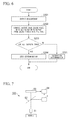
- FIG. 7 is a block diagram illustrating a structure of a virtual slide device in accordance with a fifth preferred embodiment of the present invention.
- FIG. 8 is a schematic view illustrating a structure of a solid-state imaging device in accordance with the related art
- FIG. 9 is a timing chart illustrating operation timings of the solid-state imaging device in accordance with the related art.
- FIG. 10 is a schematic view illustrating a structure of a color sensor to which the solid-state imaging device in accordance with the related art has been applied;
- FIG. 11 is a graph illustrating spectral characteristics of a multiband color sensor in accordance with the related art
- FIGS. 12A and 12B are timing charts illustrating operation timings of a color sensor to which the solid-state imaging device in accordance with the related art has been applied.
- FIG. 13 is a graph illustrating a relationship between an amount of light and an output when the output from gain circuits dropped to zero when a fixed quantity or more of light was irradiated onto the color sensor in accordance with the related art.
- FIG. 1 is a schematic view illustrating the structure of a color sensor 1 in accordance with the first preferred embodiment of the present invention.
- the color sensor 1 includes integrated circuit units 11 - 1 to 11 - 6 , gain circuits 12 - 1 to 12 - 6 , integration time calculation units 13 - 1 to 13 - 6 , gain calculation units 14 - 1 to 14 - 6 , a drive control circuit 15 , a saturation determination unit 16 , and output terminals 17 - 1 to 17 - 6 .
- the integrated circuit units 11 - 1 to 11 - 5 include pixels 111 - 1 to 111 - 5 (i.e., measurement pixels) that detect spectrum information about a subject by dividing it into respective wavelength transmission bands, reference voltage terminals 112 - 1 to 112 - 5 , switching elements 113 - 1 to 113 - 5 , capacitance elements 114 - 1 to 114 - 5 , and operational amplifiers 115 - 1 to 115 - 5 .
- the integrated circuit unit 11 - 6 includes a pixel 111 - 6 (i.e., a reference pixel) that detects light from a subject, a reference voltage terminal 112 - 6 , a switching element 113 - 6 , a capacitance element 114 - 6 , and an operational amplifier 115 - 6 . Note that portions formed by the reference voltage terminals 112 - 1 to 112 - 6 , switching elements 113 - 1 to 113 - 6 , capacitance elements 114 - 1 to 114 - 6 , and operational amplifiers 115 - 1 to 115 - 6 are called read circuits 110 - 1 to 110 - 6 .
- the pixel 111 - 1 provided in the integrated circuit unit 11 - 1 is a pixel on which a filter that transmits violet light has been coated so that it detects violet light.
- the pixel 111 - 2 provided in the integrated circuit unit 11 - 2 is a pixel on which a filter that transmits blue light has been coated so that it detects blue light.
- the pixel 111 - 3 provided in the integrated circuit unit 11 - 3 is a pixel on which a filter that transmits green light has been coated so that it detects green light.
- the pixel 111 - 4 provided in the integrated circuit unit 11 - 4 is a pixel on which a filter that transmits yellow light has been coated so that it detects yellow light.
- the pixel 111 - 5 provided in the integrated circuit unit 11 - 5 is a pixel on which a filter that transmits red light has been coated so that it detects red light.
- the pixel 111 - 6 provided in the integrated circuit unit 11 - 6 is a pixel on which no filter has been coated so that it detects all light.
- the color sensor 1 irradiates light from a subject (i.e., a test specimen) onto the pixels 111 - 1 to 111 - 6 . It also controls the integration time (i.e., a predetermined measurement time) in the switching elements 113 - 1 to 113 - 6 using as a reference a reference voltage which is applied to the reference voltage terminals 112 - 1 to 112 - 6 , and integrates the light from the subject as voltage changes that correspond to the photoelectric current in the capacitance elements 114 - 1 to 114 - 6 . It then outputs the results to output terminals of the operational amplifiers 115 - 1 to 115 - 6 . These outputs are the changes in voltage that correspond to the amount of light irradiated onto the pixels 111 - 1 to 111 - 5 .
- the color sensor 1 amplifies the output changes from the output terminals of the operational amplifiers 115 - 1 to 115 - 5 using the gain circuits 12 - 1 to 12 - 5 (i.e., measurement signal generation circuits) while removing switching noise therefrom, and then reads them.
- the color sensor 1 amplifies the output change from the output terminal of the operational amplifier 115 - 6 using the gain circuit 12 - 6 (i.e., a reference signal generation circuit) while removing switching noise therefrom, and then reads it.
- the integration times of each of the integrated circuit units 11 - 1 to 11 - 6 are calculated by the integration time calculation units 13 - 1 to 13 - 6 using information sent from the drive control circuit 15 .
- the gains of the respective gain circuits 12 - 1 to 12 - 6 are calculated by the gain calculation units 14 - 1 to 14 - 6 using information sent from the drive control circuit 15 .
- output signals that correspond to the integration time and the gain that are set by the integration time calculation units 13 - 1 to 13 - 6 and the gain calculation units 14 - 1 to 14 - 6 are output from the output terminals 17 - 1 to 17 - 6 .
- Output terminals of the gain circuits 12 - 1 to 12 - 6 are connected to the saturation determination unit 16 , and output signals from the gain circuits 12 - 1 to 12 - 6 are input into the saturation determination unit 16 .
- the saturation determination unit 16 Based on the output signals (i.e., the measurement signals) input from the gain circuits 12 - 1 to 12 - 5 and on the output signals (i.e., the reference signal) input from the gain circuit 12 - 1 , the saturation determination unit 16 performs saturation determination processing to determine whether or not the integrated circuit units 11 - 1 to 11 - 6 are in a saturated state.
- a saturated state is a state in which the amount of light of the wavelength component that is irradiated onto the color sensor 1 is equal to or more than a fixed amount of light, and in which the amount of light able to be detected by the integrated circuit units 11 - 1 to 11 - 6 has been exceeded and the output voltage values from the integrated circuit units 11 - 1 to 11 - 6 are saturated.
- the output voltage values from the integrated circuit units 11 - 1 to 11 - 6 at this time are taken as the saturation output.
- the processing steps of this saturation determination processing are described below.
- the drive control circuit 15 controls each unit provided in the color sensor 1 . By employing this structure, the color sensor 1 is able to acquire spectrum information about a subject based on output signals from the gain circuits 12 - 1 to 12 - 5 .
- FIG. 2 is a schematic view illustrating the placement of the pixels 111 - 1 to 111 - 6 provided in the color sensor 1 in accordance with the first preferred embodiment of the present invention.
- the pixel 111 - 6 on which no filter has been coated so that it is able to detect all of the light is placed on the top left side.
- the pixel 111 - 1 on which a filter that transmits violet light has been coated so that it is able to detect violet light is placed on the top right side.
- the pixel 111 - 2 on which a filter that transmits blue light has been coated so that it is able to detect blue light is placed in the top center.
- the pixel 111 - 3 on which a filter that transmits green light has been coated so that it is able to detect green light is placed in the bottom center.
- the pixel 111 - 4 on which a filter that transmits yellow light has been coated so that it is able to detect yellow light is placed on the bottom right side.
- the pixel 111 - 5 on which a filter that transmits red light has been coated so that it is able to detect red light is placed on the bottom left side.
- the placement of the pixels 111 - 1 to 111 - 6 is not limited to the placement shown in the drawing, and other desired placements may also be used.
- FIG. 3 is a graph illustrating the spectral characteristics of the pixels 111 - 1 to 111 - 6 in accordance with the first preferred embodiment of the present invention.
- This graph shows a curve 1001 that shows the transmittance of a color filter that has been coated on the pixel 111 - 1 that detects violet light, a curve 1002 that shows the transmittance of a color filter that has been coated on the pixel 111 - 2 that detects blue light, a curve 1003 that shows the transmittance of a color filter that has been coated on the pixel 111 - 3 that detects green light, a curve 1004 that shows the transmittance of a color filter that has been coated on the pixel 111 - 4 that detects yellow light, a curve 1005 that shows the transmittance of a color filter that has been coated on the pixel 111 - 5 that detects red light, and a curve 1006 that shows the transmittance of light when no filter has been coated on the pixel.
- the wavelengths of the light transmitted through each color filter are different.
- the light transmittance when no filter was coated was higher across all of the wavelength bands compared to the transmittance when a filter was coated. Because of this, compared with the outputs from the pixels 111 - 1 to 111 - 5 on which filters were coated, the output from the pixel 111 - 6 on which no filter was coated showed the highest output changes irrespective of the wavelength of the irradiated light.
- FIG. 4 is a graph illustrating the output voltage values of the integrated circuit units 11 - 1 to 11 - 6 during the time periods T 2 and T 3 , and changes in the output voltage values of the integrated circuit units 11 - 1 to 11 - 6 during the time period T 3 .
- the time periods T 2 and T 3 are the same periods as the time periods T 2 and T 3 shown in FIG. 9 .
- the changes in the output voltage values of the integrated circuit units 11 - 1 to 11 - 6 during the time period T 3 correspond to the output voltage values of the gain circuits 12 - 1 to 12 - 6 .
- FIG. 4 ( 1 ) is a graph illustrating the output voltage value of the integrated circuit unit 11 - 6 which has the pixel 111 - 6 that detects the light of all of the colors.
- FIG. 4 ( 2 ) is a graph illustrating the output voltage value of the integrated circuit unit 11 - 5 which has the pixel 111 - 5 that detects red light.
- FIG. 4 ( 3 ) is a graph illustrating the output voltage value of the integrated circuit unit 11 - 2 which has the pixel 111 - 2 that detects blue light.
- FIG. 4 ( 4 ) is a graph illustrating the output voltage value of the integrated circuit unit 11 - 1 which has the pixel 111 - 1 that detects violet light.
- FIG. 4 ( 5 ) is a graph illustrating the output voltage value of the integrated circuit unit 11 - 3 which has the pixel 111 - 3 that detects green light.
- FIG. 4 ( 6 ) is a graph illustrating the output voltage value of the integrated circuit unit 11 - 4 which has the pixel 111 - 4 that detects yellow light.
- the output changes from the integration circuit unit 11 - 6 which has the pixel 111 - 6 that detects light of all of the colors that are shown in FIG. 4 ( 1 ), and the output changes from the integration circuit unit 11 - 3 which has the pixel 111 - 3 that detects green light that are shown in FIG. 4 ( 5 ) are both zero, while the other output changes are not zero.
- the output voltage of the gain circuit 12 - 3 which reads the output changes of the integrated circuit unit 11 - 3 which has the pixel 111 - 3 that detects green light.
- the output voltage values of the gain circuits 12 - 1 , 12 - 2 , 12 - 4 , and 12 - 5 which read the output changes of the integrated circuit units 11 - 1 , 11 - 2 , 11 - 4 , and 11 - 5 which have the other pixels 111 - 1 , 111 - 2 , 111 - 4 , and 111 - 5 are not zero. Namely, the values of the output voltages of the gain circuits 12 - 1 , 12 - 2 , 12 - 4 , and 12 - 5 are larger than the value of the output voltage of the gain circuit 12 - 6 .
- the transmittance of the light when no filter is coated is higher across all wavelength bands than the transmittance when a color filter was coated. Because of this, in cases in which saturation has not occurred, the output voltage value of the gain circuit 12 - 6 which reads the output changes of the integrated circuit unit 11 - 6 which has the pixel 111 - 6 on which no filter has been coated shows the highest output change irrespective of the wavelength of the irradiated light compared with the values of the output voltages of the gain circuits 12 - 1 to 12 - 5 which read the output changes of the integrated circuit units 11 - 1 to 11 - 5 that have the pixels 111 - 1 to 111 - 5 on which filters have been coated.
- FIG. 5 is a flowchart illustrating the processing steps of the saturation determination processing of the saturation determination unit 16 in accordance with the first preferred embodiment of the present invention.
- step S 101 the saturation determination unit 16 acquires output voltage values from the gain circuits 12 - 1 to 12 - 5 that read output changes from the integrated circuit units 11 - 1 to 11 - 5 that have the pixels 111 - 1 to 111 - 5 on which filters have been coated, and an output voltage value from the gain circuit 12 - 6 that reads the output change from the integrated circuit unit 11 - 6 that has the pixel 111 - 6 that detects light of all of the colors and on which a filter has not been coated. Thereafter, the saturation determination unit 16 moves to the processing of step S 102 .
- step S 102 the saturation determination unit 16 compares the output voltage values of the gains circuits 12 - 1 to 12 - 5 that were acquired in step S 101 with the value of the output voltage from the gain circuit 12 - 6 . Thereafter, the saturation determination unit 16 moves to the processing of step S 103 .
- step S 103 if, based on the result of the comparison in step S 102 , the value of any of the output voltages from the gain circuits 12 - 1 to 12 - 5 is greater than the value of the output voltage from the gain circuit 12 - 6 , the saturation determination unit 16 determines that saturated output is contained therein and that a saturation state has been reached. Thereafter, the saturation determination processing is ended. If, however, the saturation determination unit 16 determines in the saturation determination processing that a saturation state has not been reached, it determines that the spectrum information acquired at this time is invalid.
- the saturation determination unit 16 the output voltage values from the gain circuits 12 - 1 to 12 - 5 that read changes in output from the integrated circuit units 11 - 1 to 11 - 5 that have the pixels 111 - 1 to 111 - 5 on which filters have been coated with the output voltage value from the gain circuit 12 - 6 that reads the change in output from the integrated circuit unit 11 - 6 that has the pixel 111 - 6 on which a filter has not been coated. If the value of any of the output voltages from the gain circuits 12 - 1 to 12 - 5 is greater than the value of the output voltage from the gain circuit 12 - 6 , the saturation determination unit 16 determines that a saturation state has been reached. If, however, the saturation determination unit 16 determines in the saturation determination processing that a saturation state has not been reached, it determines that the spectrum information acquired at this time is invalid. As a result of this procedure, the color sensor 1 is able to accurately acquire spectrum information.
- a second preferred embodiment of the present invention will now be described.
- the point of difference between the second preferred embodiment and the first preferred embodiment is that, in the saturation processing of the second preferred embodiment, when the values of the output voltages from the gain circuits 12 - 1 to 12 - 5 that read the changes in output from the integrated circuit units 11 - 1 to 11 - 5 that have the pixels 111 - 1 to 111 - 5 on which filters have been coated are zero, then a determination is made as to whether or not this output voltage value is a correct output voltage value.
- the structure of the color sensor 1 of the second preferred embodiment is the same as the structure of the color sensor 1 of the first preferred embodiment.
- FIG. 6 is a flowchart illustrating the processing steps of the saturation determination processing of the saturation determination unit 16 in accordance with the second preferred embodiment of the present invention.
- steps S 201 to S 202 is the same as the processing of steps S 201 to S 202 of the first preferred embodiment.
- step S 203 based on the result of the comparison in step S 202 , the determination processing unit 16 determines whether or not the values of the output voltages from the gain circuits 12 - 1 to 12 - 5 that read output changes from the integrated circuit units 11 - 1 to 11 - 5 that have the pixels 111 - 1 to 111 - 5 on which filters have been coated, and the value of the output voltage from the gain circuit 12 - 6 that reads output changes in the integrated circuit unit 11 - 6 that has the pixel 111 - 6 on which a filter has not been coated are all zero.
- the saturation determination unit 16 determines that the values of the output voltages from the gain circuits 12 - 1 to 12 - 5 and the value of the output voltage from the gain circuit 12 - 6 are all zero, it moves to the processing of step S 204 , while in all other cases it moves to the processing of step S 205 .
- step S 204 the saturation determination unit 16 determines that the values of the output voltages from the gain circuits 12 - 1 to 12 - 5 and the value of the output voltage from the gain circuit 12 - 6 are all zero (i.e., are a minimum value output). Namely, the saturation determination unit 16 determines that the values of the output voltage from the gain circuits 12 - 1 to 12 - 5 and the value of the output voltage from the gain circuit 12 - 6 are correct values. Thereafter, the processing is ended.
- step S 205 is the same as the processing of step S 103 of the first preferred embodiment.
- the second preferred embodiment of the present invention when there is a value of zero for the output voltage from the gain circuit 12 - 6 that reads output changes in the integrated circuit unit 11 - 6 that has the pixel 111 - 6 on which a filter has not been coated, it is possible to correctly determine whether the value of the output voltage is zero because the amount of light irradiated onto the color sensor 1 was too great and caused saturation to occur, or whether the value of the output voltage is zero because the amount of light irradiated onto the color sensor 1 was too small. As a consequence, it is possible to acquire spectrum information more accurately.
- a third preferred embodiment of the present invention will now be described.
- the point of difference between the third preferred embodiment and the first preferred embodiment is that, in the third preferred embodiment, when the saturation determination unit 16 has determined in the saturation determination processing that a state of saturation has been reached, the drive control circuit 15 lowers the photosensitivity of each of the integrated circuit units 11 - 1 to 11 - 6 so that the state of saturation is terminated, and spectrum information is once again acquired.
- the method used to lower the photosensitivity of the respective integrated circuit units 11 - 1 to 11 - 6 may be one in which, for example, the drive control circuit 15 controls the gain values calculated by the gain calculation units 14 - 1 to 14 - 6 such that these values are small.
- the drive control circuit 15 lowers the photosensitivity of each of the integrated circuit units 11 - 1 to 11 - 6 so that the state of saturation is terminated, and spectrum information is once again acquired. As a result, the color sensor 1 is able to acquire spectrum information more accurately.
- a fourth preferred embodiment of the present invention will now be described.
- the point of difference between the fourth preferred embodiment and the second preferred embodiment is that, in the fourth preferred embodiment, when the saturation determination unit 16 has determined in the saturation determination processing that the value of the voltage output is zero because a small amount of light is irradiated onto the color sensor 1 , the drive control circuit 15 raises the photosensitivity of each of the integrated circuit units 11 - 1 to 11 - 6 , and once again acquires the spectrum information.
- the method used to raise the photosensitivity of the respective integrated circuit units 11 - 1 to 11 - 6 may be one in which, for example, the drive control circuit 15 controls the gain values calculated by the gain calculation units 14 - 1 to 14 - 6 such that these values are large.
- the drive control circuit 15 raises the photosensitivity of each of the integrated circuit units 11 - 1 to 11 - 6 , and once again acquires the spectrum information. As a result, the color sensor 1 is able to acquire spectrum information more accurately.
- FIG. 7 is a block diagram illustrating the structure of a virtual slide device in accordance with the fifth preferred embodiment of the present invention.
- a virtual slide device 500 includes a color sensor 1 , an objective lens 81 , a half-mirror 82 , an RGB image sensor 83 , and an image processing unit 84 .
- the color sensor 1 is the same as any one of the color sensors 1 described in the first through fourth preferred embodiments, and is able to more accurately acquire spectrum information about a sample.
- the objective lens 81 condenses light that is irradiated onto a sample.
- the half-mirror 82 splits the light from the objective lens in the directions of the color sensor 1 and the RGB image sensor 83 .
- the RGB image sensor 83 generates images based on images of a subject photographed via the objective lens 81 and the half-mirror 82 .
- the image processing unit 84 performs image processing such as corrections and the like on images acquired by the RGB image sensor 83 based on spectrum information for the sample acquired by the color sensor 1 .
- the color sensor 1 is able to acquire spectrum information about a subject more accurately.
- the image processing unit 84 is able to perform image processing such as corrections and the like more accurately on images acquired by the RGB image sensor 83 .
- the color sensor 1 includes the five pixels 111 - 1 to 111 - 5 that serve as pixels on which filters have been coated, however, this invention is not limited to this and it is also possible for the color sensor to be simply provided with a plurality of pixels on which filters have been coated.
Landscapes
- Physics & Mathematics (AREA)
- Spectroscopy & Molecular Physics (AREA)
- General Physics & Mathematics (AREA)
- Engineering & Computer Science (AREA)
- Power Engineering (AREA)
- Spectrometry And Color Measurement (AREA)
- Color Television Image Signal Generators (AREA)
- Photometry And Measurement Of Optical Pulse Characteristics (AREA)
Abstract
Description
V1=Vr1+(Ipd×TINTGW)/C0 (1)
V1=Vr1+(Ipd×TINTGW)/C0+Vn (2)
V1=Vr1+(Ipd×TINTG)/C0+Vn (3)
V2=Vr3−(C1/C2)×(Ipd×TINTG)/C0 (4)
Vout=Vr3−(C1/C2)×(Ipd×TINTG)/C0 (5)
Claims (7)
Applications Claiming Priority (2)
| Application Number | Priority Date | Filing Date | Title |
|---|---|---|---|
| JP2010-215905 | 2010-09-27 | ||
| JP2010215905A JP5757711B2 (en) | 2010-09-27 | 2010-09-27 | Spectral information measurement method, color sensor, and virtual slide device |
Publications (2)
| Publication Number | Publication Date |
|---|---|
| US20120075631A1 US20120075631A1 (en) | 2012-03-29 |
| US8884210B2 true US8884210B2 (en) | 2014-11-11 |
Family
ID=45870350
Family Applications (1)
| Application Number | Title | Priority Date | Filing Date |
|---|---|---|---|
| US13/238,542 Active 2032-12-09 US8884210B2 (en) | 2010-09-27 | 2011-09-21 | Spectrum information measurement method, color sensor and virtual slide device |
Country Status (3)
| Country | Link |
|---|---|
| US (1) | US8884210B2 (en) |
| JP (1) | JP5757711B2 (en) |
| CN (1) | CN102445272A (en) |
Citations (9)
| Publication number | Priority date | Publication date | Assignee | Title |
|---|---|---|---|---|
| JPS63288580A (en) | 1988-03-28 | 1988-11-25 | Minolta Camera Co Ltd | Image sensor |
| JPH05207220A (en) | 1992-01-29 | 1993-08-13 | Olympus Optical Co Ltd | Solid-state image pickup device and its driving system |
| US20020044209A1 (en) * | 2000-10-18 | 2002-04-18 | Sony Corporation | Solid-state image pickup device |
| US20030086008A1 (en) * | 2001-11-08 | 2003-05-08 | Canon Kabushiki Kaisha | Image pick-up apparatus |
| US20050248667A1 (en) * | 2004-05-07 | 2005-11-10 | Dialog Semiconductor Gmbh | Extended dynamic range in color imagers |
| WO2006004096A2 (en) | 2004-07-06 | 2006-01-12 | Matsushita Electric Industrial Co Ltd | Solid-state imaging device |
| JP2007336157A (en) | 2006-06-14 | 2007-12-27 | Olympus Corp | Solid-state imaging apparatus |
| JP2008022521A (en) | 2006-06-14 | 2008-01-31 | Toshiba Corp | Solid-state image sensor |
| US20080130073A1 (en) * | 2006-12-01 | 2008-06-05 | Compton John T | Light sensitivity in image sensors |
-
2010
- 2010-09-27 JP JP2010215905A patent/JP5757711B2/en not_active Expired - Fee Related
-
2011
- 2011-09-21 US US13/238,542 patent/US8884210B2/en active Active
- 2011-09-22 CN CN201110284118.8A patent/CN102445272A/en active Pending
Patent Citations (9)
| Publication number | Priority date | Publication date | Assignee | Title |
|---|---|---|---|---|
| JPS63288580A (en) | 1988-03-28 | 1988-11-25 | Minolta Camera Co Ltd | Image sensor |
| JPH05207220A (en) | 1992-01-29 | 1993-08-13 | Olympus Optical Co Ltd | Solid-state image pickup device and its driving system |
| US20020044209A1 (en) * | 2000-10-18 | 2002-04-18 | Sony Corporation | Solid-state image pickup device |
| US20030086008A1 (en) * | 2001-11-08 | 2003-05-08 | Canon Kabushiki Kaisha | Image pick-up apparatus |
| US20050248667A1 (en) * | 2004-05-07 | 2005-11-10 | Dialog Semiconductor Gmbh | Extended dynamic range in color imagers |
| WO2006004096A2 (en) | 2004-07-06 | 2006-01-12 | Matsushita Electric Industrial Co Ltd | Solid-state imaging device |
| JP2007336157A (en) | 2006-06-14 | 2007-12-27 | Olympus Corp | Solid-state imaging apparatus |
| JP2008022521A (en) | 2006-06-14 | 2008-01-31 | Toshiba Corp | Solid-state image sensor |
| US20080130073A1 (en) * | 2006-12-01 | 2008-06-05 | Compton John T | Light sensitivity in image sensors |
Non-Patent Citations (2)
| Title |
|---|
| Japanese Office Action dated Mar. 4, 2014, issued in corresponding Japanese Patent Application No. 2010-215905 with English translation (8 pages). |
| Office Action dated Sep. 2, 2014, issued in corresponding Japanese application No. 2010-215905, with English Translation. |
Also Published As
| Publication number | Publication date |
|---|---|
| US20120075631A1 (en) | 2012-03-29 |
| CN102445272A (en) | 2012-05-09 |
| JP5757711B2 (en) | 2015-07-29 |
| JP2012073035A (en) | 2012-04-12 |
Similar Documents
| Publication | Publication Date | Title |
|---|---|---|
| US10412349B2 (en) | Image sensor including phase detection pixel | |
| US8125543B2 (en) | Solid-state imaging device and imaging apparatus with color correction based on light sensitivity detection | |
| US7649559B2 (en) | Amplifier offset cancellation devices, systems, and methods | |
| JP4386096B2 (en) | Image input processing apparatus and method | |
| US20180035057A1 (en) | Systems and Methods for Photometric Normalization in Array Cameras | |
| EP3093819A2 (en) | Imaging apparatus, imaging system, and signal processing method | |
| EP3430800B1 (en) | High dynamic range imaging sensor array | |
| JP5946421B2 (en) | Imaging apparatus and control method thereof | |
| US9267840B2 (en) | Photoelectric conversion apparatus that amplifies reference voltages corresponding to pixel signals of different colors at different gains | |
| US10033951B2 (en) | Image sensor that performs different readout operations and image capturing apparatus including image sensor | |
| US10205898B2 (en) | Minimizing a data pedestal level in an image sensor | |
| US10063762B2 (en) | Image sensor and driving method thereof, and image capturing apparatus with output signal control according to color | |
| EP3044872B1 (en) | Amplifier adapted for cmos imaging sensors | |
| JP2006005520A (en) | Imaging device | |
| EP2538659B1 (en) | Image pickup apparatus | |
| KR20150067392A (en) | Solid-state image pickup device and image pickup apparatus | |
| EP1943831B1 (en) | Image sensor | |
| US10313617B2 (en) | Image capturing apparatus, control method for the same, and storage medium | |
| US20170026591A1 (en) | Image sensor | |
| JP2013083876A (en) | Solid-state imaging device and camera module | |
| WO2012015628A2 (en) | Method for reducing image artifacts produced by a cmos camera | |
| US11778346B2 (en) | Image processing device, image processing method, and storage medium | |
| US7242429B1 (en) | Method for cancellation of the effect of charge feedthrough on CMOS pixel output | |
| CN110214444B (en) | Back Illuminated Global Shutter Imaging Array | |
| US8884210B2 (en) | Spectrum information measurement method, color sensor and virtual slide device |
Legal Events
| Date | Code | Title | Description |
|---|---|---|---|
| AS | Assignment |
Owner name: OLYMPUS CORPORATION, JAPAN Free format text: ASSIGNMENT OF ASSIGNORS INTEREST;ASSIGNOR:FUKUNAGA, YASUHIRO;REEL/FRAME:026992/0593 Effective date: 20110824 |
|
| STCF | Information on status: patent grant |
Free format text: PATENTED CASE |
|
| FEPP | Fee payment procedure |
Free format text: PAYOR NUMBER ASSIGNED (ORIGINAL EVENT CODE: ASPN); ENTITY STATUS OF PATENT OWNER: LARGE ENTITY |
|
| AS | Assignment |
Owner name: OLYMPUS CORPORATION, JAPAN Free format text: CHANGE OF ADDRESS;ASSIGNOR:OLYMPUS CORPORATION;REEL/FRAME:039344/0502 Effective date: 20160401 |
|
| MAFP | Maintenance fee payment |
Free format text: PAYMENT OF MAINTENANCE FEE, 4TH YEAR, LARGE ENTITY (ORIGINAL EVENT CODE: M1551) Year of fee payment: 4 |
|
| MAFP | Maintenance fee payment |
Free format text: PAYMENT OF MAINTENANCE FEE, 8TH YEAR, LARGE ENTITY (ORIGINAL EVENT CODE: M1552); ENTITY STATUS OF PATENT OWNER: LARGE ENTITY Year of fee payment: 8 |