US8880005B2 - Transceiver with cascaded phase-locked loops - Google Patents
Transceiver with cascaded phase-locked loops Download PDFInfo
- Publication number
- US8880005B2 US8880005B2 US11/685,288 US68528807A US8880005B2 US 8880005 B2 US8880005 B2 US 8880005B2 US 68528807 A US68528807 A US 68528807A US 8880005 B2 US8880005 B2 US 8880005B2
- Authority
- US
- United States
- Prior art keywords
- frequency signal
- transceiver
- signal
- signal generator
- phase
- Prior art date
- Legal status (The legal status is an assumption and is not a legal conclusion. Google has not performed a legal analysis and makes no representation as to the accuracy of the status listed.)
- Active, expires
Links
Images


Classifications
-
- H—ELECTRICITY
- H04—ELECTRIC COMMUNICATION TECHNIQUE
- H04L—TRANSMISSION OF DIGITAL INFORMATION, e.g. TELEGRAPHIC COMMUNICATION
- H04L7/00—Arrangements for synchronising receiver with transmitter
- H04L7/02—Speed or phase control by the received code signals, the signals containing no special synchronisation information
- H04L7/033—Speed or phase control by the received code signals, the signals containing no special synchronisation information using the transitions of the received signal to control the phase of the synchronising-signal-generating means, e.g. using a phase-locked loop
- H04L7/0331—Speed or phase control by the received code signals, the signals containing no special synchronisation information using the transitions of the received signal to control the phase of the synchronising-signal-generating means, e.g. using a phase-locked loop with a digital phase-locked loop [PLL] processing binary samples, e.g. add/subtract logic for correction of receiver clock
-
- H—ELECTRICITY
- H03—ELECTRONIC CIRCUITRY
- H03L—AUTOMATIC CONTROL, STARTING, SYNCHRONISATION, OR STABILISATION OF GENERATORS OF ELECTRONIC OSCILLATIONS OR PULSES
- H03L7/00—Automatic control of frequency or phase; Synchronisation
- H03L7/06—Automatic control of frequency or phase; Synchronisation using a reference signal applied to a frequency- or phase-locked loop
- H03L7/16—Indirect frequency synthesis, i.e. generating a desired one of a number of predetermined frequencies using a frequency- or phase-locked loop
- H03L7/22—Indirect frequency synthesis, i.e. generating a desired one of a number of predetermined frequencies using a frequency- or phase-locked loop using more than one loop
- H03L7/23—Indirect frequency synthesis, i.e. generating a desired one of a number of predetermined frequencies using a frequency- or phase-locked loop using more than one loop with pulse counters or frequency dividers
-
- H—ELECTRICITY
- H04—ELECTRIC COMMUNICATION TECHNIQUE
- H04B—TRANSMISSION
- H04B1/00—Details of transmission systems, not covered by a single one of groups H04B3/00 - H04B13/00; Details of transmission systems not characterised by the medium used for transmission
- H04B1/38—Transceivers, i.e. devices in which transmitter and receiver form a structural unit and in which at least one part is used for functions of transmitting and receiving
- H04B1/40—Circuits
-
- H—ELECTRICITY
- H04—ELECTRIC COMMUNICATION TECHNIQUE
- H04L—TRANSMISSION OF DIGITAL INFORMATION, e.g. TELEGRAPHIC COMMUNICATION
- H04L7/00—Arrangements for synchronising receiver with transmitter
- H04L7/0008—Synchronisation information channels, e.g. clock distribution lines
- H04L7/0012—Synchronisation information channels, e.g. clock distribution lines by comparing receiver clock with transmitter clock
-
- H—ELECTRICITY
- H04—ELECTRIC COMMUNICATION TECHNIQUE
- H04L—TRANSMISSION OF DIGITAL INFORMATION, e.g. TELEGRAPHIC COMMUNICATION
- H04L7/00—Arrangements for synchronising receiver with transmitter
- H04L7/02—Speed or phase control by the received code signals, the signals containing no special synchronisation information
- H04L7/033—Speed or phase control by the received code signals, the signals containing no special synchronisation information using the transitions of the received signal to control the phase of the synchronising-signal-generating means, e.g. using a phase-locked loop
Definitions
- the present invention relates to a transceiver.
- the present invention relates to a transceiver for example for use in a communication system.
- a transceiver is used to transmit information in a communication system, e.g. a mobile radio system or a wire-based communication system.
- the transceiver architecture for implementing broadband transmission standards such as UMTS (Universal Mobile Telecommunications System)
- UMTS Universal Mobile Telecommunications System
- the clock signal is too high to be generated directly using a crystal oscillator. Therefore, oscillator circuitry is provided to generate the clock signal.
- the interference may cause degradation in the quality of signal transmission.
- increased demands are imposed on a spectral purity of the clock signals.
- the clock signal should have a minimum amount of phase noise (jitter).
- a DLL Delay-Locked Loop
- a DLL circuit is a control loop in which an oscillator is stabilized by means of a reference frequency signal.
- the spectral purity of the clock generated in this manner is sufficient to supply a clock signal to digital blocks such as DSP (Digital Signal Processing) blocks and digital/analogue converters (DACs), for example.
- DSP Digital Signal Processing
- DACs digital/analogue converters
- the quality of a clock signal generated in a DLL is insufficient in terms of the spectral purity required. It may not be used as a reference signal for a so-called phase-locked loop (PLL) to generate the transmission signal.
- PLL phase-locked loop
- One embodiment of the invention is a transceiver comprising a first frequency signal generator and a second frequency signal generator.
- the first frequency signal generator generates a reception frequency signal, while the second frequency signal generator generates a transmission frequency signal.
- the first frequency signal generator couples to the second frequency signal generator to feed the reception frequency signal to the second frequency signal generator as a reference frequency signal.
- Another embodiment of the invention is an apparatus comprising: a modulator; a demodulator; and a cascaded phase-locked loop including a first phase-locked loop having an output and a second phase-locked loop having a reference input and a second output, wherein the output couples to the demodulator and to the reference input, and wherein the second output couples to the modulator.
- FIG. 1 illustrates a block diagram of a polar modulator of a mobile radio
- FIG. 2 illustrates a block diagram of a phase-locked loop with an external crystal oscillator for generating a reference
- FIG. 3 illustrates an embodiment of a transceiver according to the present invention.
- FIG. 1 illustrates the block diagram of a polar modulator of a mobile radio.
- the polar modulator comprises blocks, which impose increased demands on clock signals used in the system.
- a digital signal processor DSP to which input signals I and Q are applied, requires a high operating frequency DSPCLK.
- a signal I indicates the real part of a complex baseband signal.
- a second signal Q represents the imaginary part of said baseband signal.
- a digital/analogue converter DAC requires both a high operating frequency and a high spectral purity of the applied clock signals DAC CLK .
- a phase-locked loop PLL which is used as a phase modulator also requires a high operating frequency with a high spectral purity of the clock signals PLL REF .
- An output signal from the digital signal processor DSP makes use of a polar representation having an amplitude component A and a phase component F.
- the amplitude signal A is injected into a digital/analogue converter DAC and the phase signal F is injected into a phase-locked loop PLL.
- the amplitude signal A is applied to the corresponding amplitude signal input A of an amplitude modulator AM via the digital/analogue converter DAC and a filter Filt, while the output signal from the phase-locked loop is injected into the phase signal input F of the amplitude modulator AM.
- the amplitude modulator generates a radio-frequency signal RF out and provides it to its output.
- FIG. 2 shows a phased-locked loop in which the reference frequency PLLREF is fed into a phase detector PD from an external crystal oscillator XO.
- An output signal of the phase detector PD is applied to a voltage-controlled oscillator (VCO) via a loop filter LF.
- VCO voltage-controlled oscillator
- the VCO generates an output signal PLL out .
- the output signal PLL out is fed back into the phase detector PD via a divider element DIV.
- the output signal PLL put is provided at an output of the phase-locked-loop for further data processing.
- the reference signal PLL REF may be simultaneously fed into a digital signal processor DSP or a digital/analogue converter DAC as a clock signal.
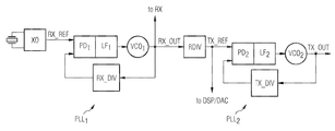
- FIG. 3 shows the block diagram of a cascaded phased-locked loop circuit.
- An external crystal oscillator XO generates a reference frequency signal RX REF which is injected into a phase detector PD 1 of the first phase-locked loop PLL 1 .
- the signal is injected into a voltage-controlled oscillator VCO 1 via a loop filter LF 1 .
- the output signal RX OUT from said oscillator is then used, on the one hand, as a clock signal for the reception path of the mobile radio circuit.
- the signal RX OUT is also referred to as a local oscillator signal.
- the signal RX OUT is fed back to the phase detector PD 1 again via a divider element RX DIV .
- the output signal RX OUT from the reception phase-locked loop PLL 1 is injected into a second phase-locked loop PLL 2 .
- the injection may be effected directly or indirectly, e.g. via a frequency divider element RDIV as shown in FIG. 3 .
- the frequency divider element RDIV provides a reference frequency signal TX REF derived from the output signal RX OUT .
- the reference frequency signal TX REF received by the second phase-locked loop PLL 2 is injected into a second phase detector PD 2 .
- the signal TX REF may be used as a clock signal for the digital signal processor DSP or for the digital/analogue converter DAC.
- the signal TX REF is injected via a loop filter LF 2 , into a voltage-controlled oscillator VCO 2 .
- the voltage-controlled oscillator VCO 2 generates an output signal TX OUT from this second phase-locked loop PLL 2 .
- the output signal TX OUT fed back to the second phase detector PD 2 via a divider element TX DIV .
- output signal TX OUT is provided at an output of the second phase-locked loop PLL 2 for further signal processing.
- the respective control loops of the two phase-locked loops PLL 1 and PLL 2 which are connected in series in cascaded fashion, are each used to ensure that the respective frequencies generated are kept stable. This results in the clock signal jitter being minimized.
- a concept of the embodiment shown in FIG. 3 is that the first frequency signal generator is used to generate a spectrally pure reference frequency signal for the second frequency signal generator.
- a greater demand is imposed on the spectral purity and bandwidth of the second frequency signal generator, which provides a clock signal for a transmission path of the transceiver circuit arrangement, than on the first frequency signal generator which provides a clock signal for a reception path of the transceiver circuit arrangement.
- These demands can be resolved by using a correspondingly high and stabilized reference frequency signal. This may be effected by virtue of the reception frequency signal being used as a reference frequency signal for the second frequency signal generator.
- the transceiver comprises a cascaded frequency signal generator circuit, which provides a spectrally pure clock signal at frequencies higher than a frequency of an external crystal oscillator with a sufficiently high spectral purity.
- the second frequency signal generator is a phase-locked loop.
- the second frequency signal generator thus generates the transmission frequency signal by comparing the latter or a multiple or divided value of the latter with the reference frequency signal.
- the phase-locked loop can generate a stable output signal, that is to say a stable transmission frequency signal, at different frequencies.
- the first frequency signal generator may be a phase-locked loop.
- the first frequency signal generator can advantageously generate a stable output signal, that is to say a stable reception frequency signal, at different frequencies.
- the transceiver includes a crystal oscillator, which is coupled to the first frequency signal generator in order to supply a frequency signal to the latter as a first reference frequency signal.
- the first frequency signal generator thus has a very stable first reference frequency signal as a reference for generating the reception frequency signal.
- An output of the first frequency signal generator connects to an input of the second frequency signal generator via a frequency divider in order to inject the reception frequency signal into the second frequency signal generator as a reference frequency signal.
- the reference frequency signal for the second frequency signal generator may thus be supplied to the second frequency signal generator at different frequencies and, in particular, at a frequency that differs from the frequency of the reception frequency signal.
- the frequency divider is arranged, so that the reference frequency signal is divided down to a frequency depending on the use of the output signals, e.g. between 100 MHz and 300 MHz.
- the transceiver is thus operable in mobile radio systems, for example UMTS or in a wireline communication system.
- the reception frequency signal is simultaneously a clock signal for a reception path of the transceiver circuit arrangement.
- the transmission frequency signal is a second clock signal in a transmission path of the transceiver circuit arrangement.
- the output of the first phase-locked loop PLL 1 couples to a demodulator in a receiption path of the transceiver.
- the second phase-locked loop PLL 2 couples to a modulator in a transmit path of the transceiver.
Abstract
Description
Claims (7)
Priority Applications (2)
| Application Number | Priority Date | Filing Date | Title |
|---|---|---|---|
| US14/516,188 US20150103966A1 (en) | 2006-03-14 | 2014-10-16 | Transceiver |
| US15/176,706 US9948450B2 (en) | 2006-03-14 | 2016-06-08 | Frequency generator |
Applications Claiming Priority (3)
| Application Number | Priority Date | Filing Date | Title |
|---|---|---|---|
| DE102006011682 | 2006-03-14 | ||
| DE102006011682.8 | 2006-03-14 | ||
| DE200610011682 DE102006011682B4 (en) | 2006-03-14 | 2006-03-14 | Transceiver circuitry |
Related Child Applications (1)
| Application Number | Title | Priority Date | Filing Date |
|---|---|---|---|
| US14/516,188 Continuation US20150103966A1 (en) | 2006-03-14 | 2014-10-16 | Transceiver |
Publications (2)
| Publication Number | Publication Date |
|---|---|
| US20070275672A1 US20070275672A1 (en) | 2007-11-29 |
| US8880005B2 true US8880005B2 (en) | 2014-11-04 |
Family
ID=38438169
Family Applications (3)
| Application Number | Title | Priority Date | Filing Date |
|---|---|---|---|
| US11/685,288 Active 2032-12-31 US8880005B2 (en) | 2006-03-14 | 2007-03-13 | Transceiver with cascaded phase-locked loops |
| US14/516,188 Abandoned US20150103966A1 (en) | 2006-03-14 | 2014-10-16 | Transceiver |
| US15/176,706 Active US9948450B2 (en) | 2006-03-14 | 2016-06-08 | Frequency generator |
Family Applications After (2)
| Application Number | Title | Priority Date | Filing Date |
|---|---|---|---|
| US14/516,188 Abandoned US20150103966A1 (en) | 2006-03-14 | 2014-10-16 | Transceiver |
| US15/176,706 Active US9948450B2 (en) | 2006-03-14 | 2016-06-08 | Frequency generator |
Country Status (2)
| Country | Link |
|---|---|
| US (3) | US8880005B2 (en) |
| DE (1) | DE102006011682B4 (en) |
Cited By (2)
| Publication number | Priority date | Publication date | Assignee | Title |
|---|---|---|---|---|
| US20150103966A1 (en) * | 2006-03-14 | 2015-04-16 | Guenter Maerzinger | Transceiver |
| US10965295B1 (en) * | 2020-05-07 | 2021-03-30 | Shenzhen GOODIX Technology Co., Ltd. | Integer boundary spur mitigation for fractional PLL frequency synthesizers |
Families Citing this family (2)
| Publication number | Priority date | Publication date | Assignee | Title |
|---|---|---|---|---|
| US20090088194A1 (en) * | 2007-09-27 | 2009-04-02 | Telefonaktiebolaget Lm Ericsson (Publ) | Single Multi-Mode Clock Source for Wireless Devices |
| US8588696B2 (en) * | 2010-06-04 | 2013-11-19 | Apple Inc. | Adaptive cellular power control |
Citations (14)
| Publication number | Priority date | Publication date | Assignee | Title |
|---|---|---|---|---|
| US5276913A (en) * | 1991-11-25 | 1994-01-04 | Motorola, Inc. | Phase-locked-loop circuit for radio transceiver |
| US5574986A (en) * | 1993-11-22 | 1996-11-12 | U.S. Philips Corporation | Telecommunication system, and a first station, a second station, and a transceiver for use in such a system |
| DE19913110C1 (en) | 1999-03-23 | 2000-11-16 | Siemens Ag | Frequency synthesizer |
| DE19938515A1 (en) | 1999-08-13 | 2001-03-22 | Siemens Ag | Frequency synthesiser for bi-directional communication system |
| US20020147014A1 (en) * | 2001-04-10 | 2002-10-10 | Roozbeh Atarius | Methods, receivers, transmitters, and systems for performing a soft hand-over of a mobile terminal between base stations that communicate using different communication channels |
| US6484038B1 (en) * | 1997-11-19 | 2002-11-19 | Ericsson Inc. | Method and apparatus for generating a plurality of reference frequencies in a mobile phone using a common crystal reference oscillator |
| US20030078011A1 (en) * | 2001-10-18 | 2003-04-24 | Integrated Programmable Communications, Inc. | Method for integrating a plurality of radio systems in a unified transceiver structure and the device of the same |
| US6621853B1 (en) * | 1998-08-28 | 2003-09-16 | Samsung Electronics Co., Ltd. | Frequency synthesizing device and method for dual frequency hopping with fast lock time |
| US20030190903A1 (en) * | 2002-07-22 | 2003-10-09 | Envara Ltd. | Zero-loss front end for wireless communication |
| US6735426B1 (en) * | 2001-01-25 | 2004-05-11 | National Semiconductor Corporation | Multiple-band wireless transceiver with quadrature conversion transmitter and receiver circuits |
| US6738602B1 (en) * | 1998-02-13 | 2004-05-18 | Infineon Technologies Ag | Integrable circuit for the frequency conditioning of radio transceiver, in particular a cordless telephone, operating in the UHF range |
| US20040152484A1 (en) * | 2001-08-07 | 2004-08-05 | Pratt Stephen J. | Multi-band tranceivers with reduced frequency sources for digital transmissions |
| US20050250464A1 (en) * | 2002-09-05 | 2005-11-10 | Koninklijke Philips Eletronics N.V. | Phase-lock loops |
| US7120427B1 (en) * | 2001-03-19 | 2006-10-10 | Cisco Systems Wireless Networking (Australia) Pty Limited | CMOS wireless transceiver with programmable characteristics |
Family Cites Families (12)
| Publication number | Priority date | Publication date | Assignee | Title |
|---|---|---|---|---|
| US4868524A (en) | 1988-10-20 | 1989-09-19 | The Johns Hopkins University | RF circuit utilizing a voltage controlled saw oscillator |
| JPH0677823A (en) | 1992-08-24 | 1994-03-18 | Oki Electric Ind Co Ltd | Frequency synthesizer |
| DE19842711C2 (en) * | 1998-09-17 | 2002-01-31 | Infineon Technologies Ag | Circuit for data signal recovery and clock signal regeneration |
| US6297702B1 (en) * | 2000-01-10 | 2001-10-02 | Honeywell International Inc. | Phase lock loop system and method |
| JP2002252559A (en) * | 2001-02-23 | 2002-09-06 | Rohm Co Ltd | Reference clock generation system |
| US7457271B2 (en) * | 2003-09-19 | 2008-11-25 | Marvell International Ltd. | Wireless local area network ad-hoc mode for reducing power consumption |
| US7747237B2 (en) | 2004-04-09 | 2010-06-29 | Skyworks Solutions, Inc. | High agility frequency synthesizer phase-locked loop |
| DE102004021224B4 (en) * | 2004-04-30 | 2006-11-09 | Advanced Micro Devices, Inc., Sunnyvale | Frequency multiplier pre-stage for N-phase locked loops |
| US7587131B1 (en) * | 2004-05-28 | 2009-09-08 | Magnum Semiconductor, Inc. | Audio clocking in video applications |
| US7301404B2 (en) * | 2005-07-21 | 2007-11-27 | Telefonaktiebolaget Lm Ericsson (Publ) | Method and apparatus for transceiver frequency synthesis |
| DE102006011682B4 (en) * | 2006-03-14 | 2015-04-09 | Intel Mobile Communications GmbH | Transceiver circuitry |
| US20080065927A1 (en) * | 2006-09-11 | 2008-03-13 | Jin-Xiao Wu | Circuit for controlling operations of universal serial bus (usb) device |
-
2006
- 2006-03-14 DE DE200610011682 patent/DE102006011682B4/en active Active
-
2007
- 2007-03-13 US US11/685,288 patent/US8880005B2/en active Active
-
2014
- 2014-10-16 US US14/516,188 patent/US20150103966A1/en not_active Abandoned
-
2016
- 2016-06-08 US US15/176,706 patent/US9948450B2/en active Active
Patent Citations (14)
| Publication number | Priority date | Publication date | Assignee | Title |
|---|---|---|---|---|
| US5276913A (en) * | 1991-11-25 | 1994-01-04 | Motorola, Inc. | Phase-locked-loop circuit for radio transceiver |
| US5574986A (en) * | 1993-11-22 | 1996-11-12 | U.S. Philips Corporation | Telecommunication system, and a first station, a second station, and a transceiver for use in such a system |
| US6484038B1 (en) * | 1997-11-19 | 2002-11-19 | Ericsson Inc. | Method and apparatus for generating a plurality of reference frequencies in a mobile phone using a common crystal reference oscillator |
| US6738602B1 (en) * | 1998-02-13 | 2004-05-18 | Infineon Technologies Ag | Integrable circuit for the frequency conditioning of radio transceiver, in particular a cordless telephone, operating in the UHF range |
| US6621853B1 (en) * | 1998-08-28 | 2003-09-16 | Samsung Electronics Co., Ltd. | Frequency synthesizing device and method for dual frequency hopping with fast lock time |
| DE19913110C1 (en) | 1999-03-23 | 2000-11-16 | Siemens Ag | Frequency synthesizer |
| DE19938515A1 (en) | 1999-08-13 | 2001-03-22 | Siemens Ag | Frequency synthesiser for bi-directional communication system |
| US6735426B1 (en) * | 2001-01-25 | 2004-05-11 | National Semiconductor Corporation | Multiple-band wireless transceiver with quadrature conversion transmitter and receiver circuits |
| US7120427B1 (en) * | 2001-03-19 | 2006-10-10 | Cisco Systems Wireless Networking (Australia) Pty Limited | CMOS wireless transceiver with programmable characteristics |
| US20020147014A1 (en) * | 2001-04-10 | 2002-10-10 | Roozbeh Atarius | Methods, receivers, transmitters, and systems for performing a soft hand-over of a mobile terminal between base stations that communicate using different communication channels |
| US20040152484A1 (en) * | 2001-08-07 | 2004-08-05 | Pratt Stephen J. | Multi-band tranceivers with reduced frequency sources for digital transmissions |
| US20030078011A1 (en) * | 2001-10-18 | 2003-04-24 | Integrated Programmable Communications, Inc. | Method for integrating a plurality of radio systems in a unified transceiver structure and the device of the same |
| US20030190903A1 (en) * | 2002-07-22 | 2003-10-09 | Envara Ltd. | Zero-loss front end for wireless communication |
| US20050250464A1 (en) * | 2002-09-05 | 2005-11-10 | Koninklijke Philips Eletronics N.V. | Phase-lock loops |
Non-Patent Citations (3)
| Title |
|---|
| Axcelerator Family PLL and Clock Management; Actel Application Note; pp. 1-7; Jun. 2003. |
| Hajimiri et al; Jitter and Phase Noise in Ring Oscillators; IEEE Journal of Solid-State Circuits; Jun. 1999: pp. 790-804; vol. 34. No. 6. |
| Reza Navid et al; Minimum Achievable Phase Noise of RC Oscillators; IEEE Journal of Solid-State Circuits; Mar. 2005; pp. 630-636; vol. 40, No. 3. |
Cited By (3)
| Publication number | Priority date | Publication date | Assignee | Title |
|---|---|---|---|---|
| US20150103966A1 (en) * | 2006-03-14 | 2015-04-16 | Guenter Maerzinger | Transceiver |
| US9948450B2 (en) | 2006-03-14 | 2018-04-17 | Intel Deutschland Gmbh | Frequency generator |
| US10965295B1 (en) * | 2020-05-07 | 2021-03-30 | Shenzhen GOODIX Technology Co., Ltd. | Integer boundary spur mitigation for fractional PLL frequency synthesizers |
Also Published As
| Publication number | Publication date |
|---|---|
| US9948450B2 (en) | 2018-04-17 |
| US20070275672A1 (en) | 2007-11-29 |
| US20160285618A1 (en) | 2016-09-29 |
| US20150103966A1 (en) | 2015-04-16 |
| DE102006011682B4 (en) | 2015-04-09 |
| DE102006011682A1 (en) | 2007-09-27 |
Similar Documents
| Publication | Publication Date | Title |
|---|---|---|
| US9160396B2 (en) | LO generation and distribution in a multi-band transceiver | |
| US8331520B2 (en) | Phase-locked loop circuit and communication apparatus | |
| US8655296B2 (en) | Frequency synthesizer and related method for generating wideband signals | |
| US7019571B2 (en) | Frequency synthesizer for a wireless communication system | |
| US6704383B2 (en) | Sample and hold type fractional-N frequency synthesizer | |
| EP2064814B1 (en) | Digital polar radiofrequency transmitting device with a radiofrequency reference oscillator and an integrated circuit comprising such device | |
| US20020136341A1 (en) | Fractional-N frequency synthesizer with fractional compensation method | |
| US9948450B2 (en) | Frequency generator | |
| US8374283B2 (en) | Local oscillator with injection pulling suppression and spurious products filtering | |
| US8013681B2 (en) | Wide spectrum radio transmit architecture | |
| US7521974B2 (en) | Translational phase locked loop using a quantized interpolated edge timed synthesizer | |
| US20120169387A1 (en) | Oscillator with external voltage control and interpolative divider in the output path | |
| US20110096864A1 (en) | Programmable digital clock control scheme to minimize spur effect on a receiver | |
| US9628066B1 (en) | Fast switching, low phase noise frequency synthesizer | |
| US20100073095A1 (en) | Frequency Synthesizer and Radio Transmitting Apparatus | |
| JP2008187556A (en) | Reception apparatus | |
| US20150188552A1 (en) | Phase locked loop and control method thereof | |
| GB2373113A (en) | Improvements in or relating to fast frequency-hopping synthesisers | |
| KR20010091693A (en) | Direct conversion receiver minimizing local oscillator leakage and method thereof | |
| US7822392B2 (en) | Frequency modulation circuit, transmission circuit and communication device | |
| JP4625030B2 (en) | Communications system | |
| KR19990061629A (en) | Phase-locked loop device for shortening the locking time | |
| US20100203852A1 (en) | Frequency modulation circuit, transmitter, and communication apparatus | |
| San et al. | Frequency Synthesis: Current Solutions and New Trends |
Legal Events
| Date | Code | Title | Description |
|---|---|---|---|
| AS | Assignment |
Owner name: INFINEON TECHNOLOGIES AG, GERMANY Free format text: ASSIGNMENT OF ASSIGNORS INTEREST;ASSIGNORS:MAERZINGER, GUENTER;ADLER, BERND;REEL/FRAME:019678/0585;SIGNING DATES FROM 20070601 TO 20070613 Owner name: INFINEON TECHNOLOGIES AG, GERMANY Free format text: ASSIGNMENT OF ASSIGNORS INTEREST;ASSIGNORS:MAERZINGER, GUENTER;ADLER, BERND;SIGNING DATES FROM 20070601 TO 20070613;REEL/FRAME:019678/0585 |
|
| AS | Assignment |
Owner name: INTEL MOBILE COMMUNICATIONS TECHNOLOGY GMBH, GERMA Free format text: ASSIGNMENT OF ASSIGNORS INTEREST;ASSIGNOR:INFINEON TECHNOLOGIES AG;REEL/FRAME:027548/0623 Effective date: 20110131 |
|
| AS | Assignment |
Owner name: INTEL MOBILE COMMUNICATIONS GMBH, GERMANY Free format text: ASSIGNMENT OF ASSIGNORS INTEREST;ASSIGNOR:INTEL MOBILE COMMUNICATIONS TECHNOLOGY GMBH;REEL/FRAME:027556/0709 Effective date: 20111031 |
|
| FEPP | Fee payment procedure |
Free format text: PAYOR NUMBER ASSIGNED (ORIGINAL EVENT CODE: ASPN); ENTITY STATUS OF PATENT OWNER: LARGE ENTITY |
|
| STCF | Information on status: patent grant |
Free format text: PATENTED CASE |
|
| AS | Assignment |
Owner name: INTEL DEUTSCHLAND GMBH, GERMANY Free format text: CHANGE OF NAME;ASSIGNOR:INTEL MOBILE COMMUNICATIONS GMBH;REEL/FRAME:037057/0061 Effective date: 20150507 |
|
| MAFP | Maintenance fee payment |
Free format text: PAYMENT OF MAINTENANCE FEE, 4TH YEAR, LARGE ENTITY (ORIGINAL EVENT CODE: M1551) Year of fee payment: 4 |
|
| AS | Assignment |
Owner name: INTEL CORPORATION, CALIFORNIA Free format text: CONFIRMATORY ASSIGNMENT EFFECTIVE AS OF JANUARY 1, 2018;ASSIGNOR:INTEL DEUTSCHLAND GMBH;REEL/FRAME:053477/0001 Effective date: 20200615 |
|
| AS | Assignment |
Owner name: APPLE INC., CALIFORNIA Free format text: ASSIGNMENT OF ASSIGNORS INTEREST;ASSIGNOR:INTEL CORPORATION;REEL/FRAME:053518/0586 Effective date: 20191130 |
|
| MAFP | Maintenance fee payment |
Free format text: PAYMENT OF MAINTENANCE FEE, 8TH YEAR, LARGE ENTITY (ORIGINAL EVENT CODE: M1552); ENTITY STATUS OF PATENT OWNER: LARGE ENTITY Year of fee payment: 8 |