US8866804B2 - Pixel structure and a driving method thereof - Google Patents
Pixel structure and a driving method thereof Download PDFInfo
- Publication number
- US8866804B2 US8866804B2 US13/146,471 US201113146471A US8866804B2 US 8866804 B2 US8866804 B2 US 8866804B2 US 201113146471 A US201113146471 A US 201113146471A US 8866804 B2 US8866804 B2 US 8866804B2
- Authority
- US
- United States
- Prior art keywords
- storage capacitor
- time period
- transistor
- capacitor
- coupled
- Prior art date
- Legal status (The legal status is an assumption and is not a legal conclusion. Google has not performed a legal analysis and makes no representation as to the accuracy of the status listed.)
- Active, expires
Links
Images


Classifications
-
- G—PHYSICS
- G06—COMPUTING OR CALCULATING; COUNTING
- G06F—ELECTRIC DIGITAL DATA PROCESSING
- G06F3/00—Input arrangements for transferring data to be processed into a form capable of being handled by the computer; Output arrangements for transferring data from processing unit to output unit, e.g. interface arrangements
- G06F3/01—Input arrangements or combined input and output arrangements for interaction between user and computer
- G06F3/03—Arrangements for converting the position or the displacement of a member into a coded form
- G06F3/033—Pointing devices displaced or positioned by the user, e.g. mice, trackballs, pens or joysticks; Accessories therefor
- G06F3/038—Control and interface arrangements therefor, e.g. drivers or device-embedded control circuitry
-
- G—PHYSICS
- G09—EDUCATION; CRYPTOGRAPHY; DISPLAY; ADVERTISING; SEALS
- G09G—ARRANGEMENTS OR CIRCUITS FOR CONTROL OF INDICATING DEVICES USING STATIC MEANS TO PRESENT VARIABLE INFORMATION
- G09G3/00—Control arrangements or circuits, of interest only in connection with visual indicators other than cathode-ray tubes
- G09G3/20—Control arrangements or circuits, of interest only in connection with visual indicators other than cathode-ray tubes for presentation of an assembly of a number of characters, e.g. a page, by composing the assembly by combination of individual elements arranged in a matrix no fixed position being assigned to or needed to be assigned to the individual characters or partial characters
- G09G3/34—Control arrangements or circuits, of interest only in connection with visual indicators other than cathode-ray tubes for presentation of an assembly of a number of characters, e.g. a page, by composing the assembly by combination of individual elements arranged in a matrix no fixed position being assigned to or needed to be assigned to the individual characters or partial characters by control of light from an independent source
- G09G3/36—Control arrangements or circuits, of interest only in connection with visual indicators other than cathode-ray tubes for presentation of an assembly of a number of characters, e.g. a page, by composing the assembly by combination of individual elements arranged in a matrix no fixed position being assigned to or needed to be assigned to the individual characters or partial characters by control of light from an independent source using liquid crystals
- G09G3/3611—Control of matrices with row and column drivers
- G09G3/3648—Control of matrices with row and column drivers using an active matrix
- G09G3/3659—Control of matrices with row and column drivers using an active matrix the addressing of the pixel involving the control of two or more scan electrodes or two or more data electrodes, e.g. pixel voltage dependant on signal of two data electrodes
-
- G—PHYSICS
- G09—EDUCATION; CRYPTOGRAPHY; DISPLAY; ADVERTISING; SEALS
- G09G—ARRANGEMENTS OR CIRCUITS FOR CONTROL OF INDICATING DEVICES USING STATIC MEANS TO PRESENT VARIABLE INFORMATION
- G09G3/00—Control arrangements or circuits, of interest only in connection with visual indicators other than cathode-ray tubes
- G09G3/20—Control arrangements or circuits, of interest only in connection with visual indicators other than cathode-ray tubes for presentation of an assembly of a number of characters, e.g. a page, by composing the assembly by combination of individual elements arranged in a matrix no fixed position being assigned to or needed to be assigned to the individual characters or partial characters
- G09G3/34—Control arrangements or circuits, of interest only in connection with visual indicators other than cathode-ray tubes for presentation of an assembly of a number of characters, e.g. a page, by composing the assembly by combination of individual elements arranged in a matrix no fixed position being assigned to or needed to be assigned to the individual characters or partial characters by control of light from an independent source
- G09G3/36—Control arrangements or circuits, of interest only in connection with visual indicators other than cathode-ray tubes for presentation of an assembly of a number of characters, e.g. a page, by composing the assembly by combination of individual elements arranged in a matrix no fixed position being assigned to or needed to be assigned to the individual characters or partial characters by control of light from an independent source using liquid crystals
-
- G—PHYSICS
- G09—EDUCATION; CRYPTOGRAPHY; DISPLAY; ADVERTISING; SEALS
- G09G—ARRANGEMENTS OR CIRCUITS FOR CONTROL OF INDICATING DEVICES USING STATIC MEANS TO PRESENT VARIABLE INFORMATION
- G09G2300/00—Aspects of the constitution of display devices
- G09G2300/04—Structural and physical details of display devices
- G09G2300/0439—Pixel structures
- G09G2300/0443—Pixel structures with several sub-pixels for the same colour in a pixel, not specifically used to display gradations
- G09G2300/0447—Pixel structures with several sub-pixels for the same colour in a pixel, not specifically used to display gradations for multi-domain technique to improve the viewing angle in a liquid crystal display, such as multi-vertical alignment [MVA]
-
- G—PHYSICS
- G09—EDUCATION; CRYPTOGRAPHY; DISPLAY; ADVERTISING; SEALS
- G09G—ARRANGEMENTS OR CIRCUITS FOR CONTROL OF INDICATING DEVICES USING STATIC MEANS TO PRESENT VARIABLE INFORMATION
- G09G2300/00—Aspects of the constitution of display devices
- G09G2300/08—Active matrix structure, i.e. with use of active elements, inclusive of non-linear two terminal elements, in the pixels together with light emitting or modulating elements
- G09G2300/0809—Several active elements per pixel in active matrix panels
- G09G2300/0814—Several active elements per pixel in active matrix panels used for selection purposes, e.g. logical AND for partial update
-
- G—PHYSICS
- G09—EDUCATION; CRYPTOGRAPHY; DISPLAY; ADVERTISING; SEALS
- G09G—ARRANGEMENTS OR CIRCUITS FOR CONTROL OF INDICATING DEVICES USING STATIC MEANS TO PRESENT VARIABLE INFORMATION
- G09G2300/00—Aspects of the constitution of display devices
- G09G2300/08—Active matrix structure, i.e. with use of active elements, inclusive of non-linear two terminal elements, in the pixels together with light emitting or modulating elements
- G09G2300/0809—Several active elements per pixel in active matrix panels
- G09G2300/0842—Several active elements per pixel in active matrix panels forming a memory circuit, e.g. a dynamic memory with one capacitor
- G09G2300/0852—Several active elements per pixel in active matrix panels forming a memory circuit, e.g. a dynamic memory with one capacitor being a dynamic memory with more than one capacitor
-
- G—PHYSICS
- G09—EDUCATION; CRYPTOGRAPHY; DISPLAY; ADVERTISING; SEALS
- G09G—ARRANGEMENTS OR CIRCUITS FOR CONTROL OF INDICATING DEVICES USING STATIC MEANS TO PRESENT VARIABLE INFORMATION
- G09G2320/00—Control of display operating conditions
- G09G2320/02—Improving the quality of display appearance
- G09G2320/028—Improving the quality of display appearance by changing the viewing angle properties, e.g. widening the viewing angle, adapting the viewing angle to the view direction
Definitions
- the present invention relates to a pixel structure and a driving method thereof, and more particularly, to a pixel structure used to minimize color washout effect and a driving method thereof.
- LCDs liquid crystal displays
- PDAs personal digital assistants
- laptop computers laptop computers
- notebook computers notebook computers
- TFT-LCDs Thin-film-transistor liquid crystal displays
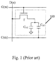
- FIG. 1 showing an equivalent circuit diagram of a pixel unit 100 on a conventional LCD panel
- the pixel units 100 on the LCD panel corresponds to a scan line G(m), a data line D(n), and a common line C(m).
- the unit 100 comprises a thin film transistor (TFT) T, a liquid crystal (LC) capacitor C LC , and a storage capacitor C ST .
- TFT T controls conduction and disconnection according to a scan signal through the scan line G(m).
- the TFT T turns on, causing data voltage applied on the data line D(n) to be delivered to the LC capacitor C LC and to the storage capacitor C ST , so that the LC capacitor C LC and the storage capacitor C ST are charged.
- FIG. 2 illustrates a waveform diagram of a scan signal applied on the pixel unit 100 shown in FIG. 1 .
- the LCD panel comprises a plurality of pixel units 100 , and each of the plurality of pixel units 100 corresponds to one of the scan lines G(m ⁇ 1) ⁇ G(m+1) and to one of the data lines D(n ⁇ 1) ⁇ D(n+1), respectively, as FIG. 2 shows.
- the common line connected to each of the plurality of pixel units 100 is omitted in FIG. 2 .
- Scan signals transmitted through each of the scan lines G(m ⁇ 1) ⁇ G(m+1) are generated sequentially.
- the scan signals are sequentially input to the neighboring scan lines G(m ⁇ 1) ⁇ G(m+1), so that the scan signals applied on the neighboring scan lines G(m ⁇ 1) ⁇ G(m+1) sequentially correspond to the high voltage level, causing the TFT T in the pixel unit 100 to conduct.
- Data voltage is stored in the storage capacitor C ST and in the LC capacitor C LC corresponding to the pixel unit 100 row by row through the data lines D(n ⁇ 1) ⁇ D(n+1) and thereby a desired gray level is shown.
- LCDs with a high contrast ratio, a swift response time, and a wide viewing angle are designed in accordance with the needs of the market.
- LCDs with a wide viewing angle can be designed with the technology like multi-domain vertically alignment (MVA), multi-domain horizontal alignment (MHA), twisted nematic plus wide viewing film (TN+film), and in-plane switching (IPS).
- MVA multi-domain vertically alignment
- MHA multi-domain horizontal alignment
- TN+film twisted nematic plus wide viewing film
- IPS in-plane switching
- the MVA technology can be implemented on TFT-LCDs to make the TFT-LCDs with a wide viewing angle
- a problem of color washout occurs, which is blamed by the public.
- the color washout is that an image displayed on a LCD panel shows different colors in different sights of viewing angles. For instance, a user may see an image with a whiter color when his/her sight is at a more slanted angle with respect to the LCD panel.
- FIG. 3 is an equivalent circuit diagram showing a pixel unit 400 having a function of compensation for color washout according to conventional technology.
- the pixel unit 400 corresponds to two scan lines G 1 ( m ) and G 2 ( m ), a common line C(m), and a data line D(n). Further, the pixel unit 400 is divided into two pixel parts 400 a and 400 b .
- Each of the pixel parts 400 a and 400 b basically comprises the pixel unit 100 shown in FIG. 1 .
- the pixel part 400 a comprises a transistor S 1 , an LC capacitor C LC1 , and a storage capacitor C ST1 .
- the pixel part 400 b comprises a transistor S 2 , an LC capacitor C LC2 , and a storage capacitor C ST2 .
- the pixel part 400 a and the pixel part 400 b correspond to the scan line G 1 ( m ) and the scan line G 2 ( m ), respectively.
- FIG. 4 illustrates waveforms of the scan signal applied on the pixel units 400 a and 400 b shown in FIG. 3 .
- the LCD panel comprises a plurality of pixel units 400 .
- the common line C(m) is omitted in FIG. 4 .
- Each of the plurality of pixel units 400 comprises two pixel parts 400 a and 400 b , as shown in FIG. 4 .
- the driving method of driving the pixel unit 400 is similar to that of driving the pixel unit 100 .
- Scan signals are sequentially input to the neighboring scan lines G 1 ( m ) ⁇ G 2 ( m +1), so that the neighboring scan lines G 1 ( m ) ⁇ G 2 ( m +1) sequentially correspond to a high voltage level in an order of G 1 ( m ) ⁇ G 2 ( m ) ⁇ G 1 ( m +1) ⁇ G 2 ( m +1), causing the TFTs in the pixel unit 400 to conduct.
- Data voltage is stored in the storage capacitors C ST1 and C ST2 and in the LC capacitors C LC1 and C LC2 corresponding to the pixel unit 400 column by column through the data lines D(n ⁇ 1) ⁇ D(n+1) and thereby a correct frame is shown.
- the method has a problem of doubling the number of the scan lines, causing the valid charging duration to be reduced to half the original one.
- such kind of technology is unable to be implemented in an LCD having a higher frame rate due to insufficient charging duration.
- the received digital image data carried by data voltage transmitted through the data lines D(n ⁇ 1) ⁇ D(n+1) has to be transformed into analog data voltage by using a gamma circuit.
- the analog data voltage corresponds to different gray levels.
- the pixel unit 400 drives LC molecules to display different gray levels in accordance with the analog data voltage transmitted through the data line. Since each of the plurality of pixel units 400 comprises two pixel parts 400 a and 400 b and gray levels of the two pixel parts 400 a and 400 b are required to be different in this technology, color washout can be solved even though a user sees on the LCD panel at different viewing angles. The reason why color washout can be solved is that the two different gray levels are complementary.
- the digital image data is input to two gamma circuits at the same time, and then the pixel parts 400 a and 400 b respectively receive different kinds of analog data voltage to increase flexibility of color correction in this pixel structure.
- An overall manufacturing cost of the circuit is increased due two gamma circuits used. Therefore, there is a need for a new pixel driving structure for solving the problem mentioned above.
- An object of the present invention is to provide a pixel structure where no additional gamma circuit needs to be disposed for minimizing color washout and a driving method thereof, and further to reduce manufacturing cost due to an additional gamma circuit used in the conventional technology.
- a pixel structure comprising a first scan line, a second scan line, and a data line.
- the pixel structure further comprises a first storage capacitor, a second storage capacitor, a first transistor, and a second transistor.
- the first storage capacitor comprises a first terminal and a second terminal, the first terminal coupled to a common line.
- the second storage capacitor comprises a first terminal and a second terminal, the first terminal coupled to the common line.
- the first transistor which comprises a first gate, a first source, and a first drain is used for conducting the data line and the first storage capacitor.
- the first gate of the first transistor is coupled to a first scan line.
- the first source and the first drain of the first transistor are coupled to a data line and to the second terminal of the first storage capacitor, respectively.
- the second transistor comprises a second gate, a second source, and a second drain.
- the second gate of the second transistor is coupled to a second scan line.
- the second source and the second drain of the second transistor are coupled to the second terminal of the first storage capacitor and to the second terminal of the second storage capacitor, respectively.
- a first polarity voltage applied on the data line is stored into the first storage capacitor during a first time period which the first transistor is turned on.
- the first storage capacitor discharges due to a connection between the first capacitor and the second capacitor during a second time period which the second transistor is turned on.
- a method of driving a pixel comprises the steps of providing a pixel structure comprising a first scan line, a second scan line, and a data line, a first storage capacitor coupled to a common line via a first transistor, and a second storage capacitor one terminal coupled to the common line and the other terminal coupled to the first transistor via a second transistor; outputting a scan signal through the first scan line to the first transistor, so that a first polarity voltage applied on the data line is stored into the first storage capacitor during a first time period; outputting a scan signal through the second scan line to the second transistor, so that the first storage capacitor discharges due to a connection between the first capacitor and the second capacitor during a second time period.
- both of the first transistor and the second transistor are thin-film transistors.
- the first time period does not overlap with the second time period.
- the first time period is prior to the second time period.
- the pixel structure further comprises a liquid crystal capacitor, and one terminal of the liquid crystal capacitor is coupled to the second terminal of the first storage capacitor.
- the first scan line is coupled to the gate of the first transistor, and the second scan line is coupled to the gate of the second transistor.
- a second polarity voltage applied on the data line is stored into the first storage capacitor during a third time period which the first transistor is turned on, and the first storage capacitor discharges due to a connection between the first capacitor and the second capacitor during a fourth time period which the second transistor is turned on.
- the second time period is prior to the third time period
- the third time period is prior to the fourth time period.
- the polarity of the first polarity voltage is contrary to that of the second polarity voltage.
- the pixel structure comprises two TFTs, an LC capacitor, a first storage capacitor, and a second storage capacitor according to the present invention.
- the two TFTs are connected to two scan lines, respectively, for conducting at different timings.
- one of the TFTs stores data voltage applied on the data line into the first storage capacitor and into the LC capacitor. While the other TFT conducts, it conducts the first storage capacitor and second storage capacitor, allowing the first and second storage capacitors to perform charge sharing.
- the difference in voltage between the LC capacitor and common voltage is reduced from charge sharing and further, a color washout effect of the panel is minimized.
- FIG. 1 shows an equivalent circuit diagram of a pixel unit on a conventional LCD panel
- FIG. 2 illustrates a waveform diagram of a scan signal applied on the pixel unit shown in FIG. 1 .
- FIG. 3 is an equivalent circuit diagram showing a pixel unit having a function of compensation for color washout according to conventional technology.
- FIG. 4 illustrates waveforms of the scan signal applied on the pixel units and shown in FIG. 3 .
- FIG. 5 is an equivalent circuit diagram of a pixel unit according to an embodiment of the present invention.
- FIG. 6 illustrates a waveform diagram of a scan signal in the pixel units shown in FIG. 5 .
- FIG. 7 is a timing diagram showing that the voltage level applied on the node A varies with time.
- FIG. 5 is an equivalent circuit diagram of a pixel unit 700 according to an embodiment of the present invention.
- the pixel unit 700 comprises a first TFT S 1 , a second TFT S 2 , a first storage capacitor C ST1 , a second storage capacitor C ST2 , and an LC capacitor C LC .
- the first TFT S 1 corresponds to a first scan line G 1 ( m )
- the second TFT S 2 corresponds to a second scan line G 2 ( m ).
- the first TFT S 1 comprises a gate coupled to the first scan line G 1 ( m ), a source coupled to a data line D(n), and a drain coupled to a node A.
- the second TFT S 2 comprises a gate coupled to the second scan line G 2 ( m ), a source coupled to the node A, and a drain coupled to the storage capacitor C ST2 .
- One terminal of the storage capacitor C ST1 is coupled to the node A and the other terminal is coupled to a common line C(m).
- One terminal of the storage capacitor C ST2 is also coupled to the common line C(m) and the other terminal is coupled to the drain of the TFT S 2 .
- One terminal of the LC capacitor C LC is coupled to the node A and the other terminal is coupled to the ground.
- the common line C(m) outputs common voltage Vcom.
- the first TFT S 1 and the second TFT S 2 serving as switches, are turned on using signals transmitted through the scan lines G 1 ( m ) and G 2 ( m ) in the present embodiment.
- a detailed driving method of the pixel unit 700 is provided hereafter.
- FIG. 6 illustrates a waveform diagram of a scan signal in the pixel units 700 shown in FIG. 5 , where m represents the mth row, m+1 represents the (m+1)th row, and so forth, and n represents the nth column, n+1 represents the (n+1)th column, and so forth.
- the scan signal applied on the neighboring scan lines G 1 ( m ) and G 2 ( m ) does not achieve a high voltage level sequentially; instead, the scan signal applied on the neighboring scan lines G 1 ( m ) and G 2 ( m ) are used to driving two driving groups.
- the driving order of the first driving group is G 1 ( m ⁇ 1) ⁇ G 1 ( m ) ⁇ G 1 ( m +1); the driving order of the second driving group is G 2 ( m ⁇ 1) ⁇ G 2 ( m ) ⁇ G 2 ( m +1).
- the two groups are scanned at the same frame rate.
- an interval t 1 in the figure represents a period during which scan signals are transmitted through the first scan line G 1 ( m ).
- W 1 represents a first time period at which pulses of scan signals transmitted through the scan line G 1 ( m ) turn on the transistor.
- the interval t 1 is determined by the frame rate of the panel. For example, the interval t 1 is 1/60 second when the frame rate is 60 Hz.
- an interval t 2 represents the time difference between a period during which scan signals are transmitted through the second scan line G 2 ( m ) and a period during which scan signals are transmitted through the first scan line G 1 ( m ) in a pixel unit.
- W 2 represents a second time period at which pulses of scan signals transmitted through the scan line G 2 ( m ) turn on the transistor.
- the interval t 2 has to be smaller than the interval t 1 , and the period of the second time period W 2 has to be the same as that of the first time period W 1 (because the first time period W 1 and the second time period W 2 may overlap during different periods of time) to ensure that scan signals do not be transmitted through the first scan line G 1 ( m ) and through the second scan line G 2 ( m ) at the same time.
- the first time period W 1 at which scan signals are transmitted through the scan line G 1 ( m ) does not overlap with the second time period W 2 at which scan signals are transmitted through the scan line G 2 ( m ), and the first time period W 1 is prior to the second time period W 2 .
- the first time period W 1 and the second time period W 2 correspond to the same pixel unit 700 .
- the main object of the design is to ensure that two gray levels are shown over an interval t 1 for the pixel unit 700 . Both of the gray levels are supplemented mutually, so no color washout occurs no matter at what angle a user sees on the panel. This ensures that good image quality is maintained. In addition, color washout and brightness of the panel can both be controlled by adjusting the driving timing of the two driving groups.
- FIG. 7 is a timing diagram showing that the voltage level applied on the node A varies with time.
- the transistor S 1 in FIG. 6 conducts when scan signals are transmitted through the scan line G 1 ( m ) (corresponding to the time period W 1 in FIGS. 6 and 7 ), so that both of the LC capacitor C LC and the storage capacitor C ST1 are charged with the voltage applied on the data line D(n).
- the transistor S 2 in FIG. 6 conducts when scan signals are transmitted through the scan line G 2 ( m ) (referring to the time period W 2 in FIGS. 6 and 7 ), so that the pixel unit 700 is charged with the voltage contained in the storage capacitor C ST2 .
- charge sharing is performed between the storage capacitor C ST1 and the storage capacitor C ST2 .
- Each of the plurality of pixel units 700 receives data voltage having positive and negative polarities alternatively.
- the data voltage having a positive polarity means that the data voltage is larger than the common voltage Vcom.
- the data voltage having a negative polarity means that the data voltage is smaller than the common voltage Vcom. It means that the pixel unit 700 receives the data voltage having a positive polarity at time T 0 , receives the data voltage having a negative polarity at time T 2 , and receives the data voltage having a positive polarity at time T 4 .
- the first TFT S 1 is turned on in response to the pulse W 1 of the scan signal transmitted through the scan line G 1 ( m ), the data voltage having a positive polarity is transmitted to the storage capacitor C ST1 and to the LC capacitor C LC through the data line D(n) via the conducting first TFT S 1 , causing the voltage applied on the node A to become the voltage level V 1 according to the data voltage. Meanwhile, the alignment of the LC molecules contained in the LC capacitor C LC is adjusted according to the voltage level V 1 .
- the first TFT S 1 is turned on in response to the pulse W 1 of the scan signal (i.e., the first time period W 1 ) transmitted through the scan line G 1 ( m ), the data voltage having a negative polarity is transmitted to the storage capacitor C ST1 and the LC capacitor C LC through the data line D(n) via the turned-on first TFT S 1 , causing the voltage applied on the node A to become the voltage level V 3 according to the data voltage. Meanwhile, the alignment of the LC molecules contained in the LC capacitor C LC is adjusted according to the voltage level V 3 .
- the transistor S 2 is turned on in response to the pulse W 2 , and the polarity of the voltage stored in the storage capacitor C ST2 is always contrary to that applied on the pixel.
- the polarities of the voltage of two pixels in neighboring frames are positive and negative in turns. For instance, the voltage across the storage capacitor C ST1 of the pixel 700 is at a high voltage level while the voltage across the storage capacitor C ST2 of the pixel 700 remains at a low voltage level since the previous frame, when the first frame is shown during the period T 0 -T 2 .
- the storage capacitor C ST1 is at a low voltage level while the storage capacitor C ST2 remains at a high voltage level since the first frame, when the second frame is shown during the period T 2 -T 4 .
- the voltage level V 3 applied on the node A is negative polarity (smaller than the common voltage Vcom) and the voltage level V 2 applied on the storage capacitor C ST2 is positive polarity (larger than the common voltage Vcom) at time T 3 .
- the voltage applied on the LC capacitor C LC (i.e., the level applied on the node A) is lowered while the transistor S 2 is turned on, causing the difference in voltage between the LC capacitor C LC and the common voltage Vcom to be reduced for a while (the interval t 3 ).
- the driving method can solve the problem of color washout occurring on the panel.
- there is no need for an additional gamma circuit in the pixel unit 700 which means that color washout occurring in the panel can be solved successfully without additional cost by using the pixel unit 700 and a driving method thereof according to the present invention.
Landscapes
- Engineering & Computer Science (AREA)
- Theoretical Computer Science (AREA)
- Physics & Mathematics (AREA)
- General Physics & Mathematics (AREA)
- Chemical & Material Sciences (AREA)
- Crystallography & Structural Chemistry (AREA)
- Computer Hardware Design (AREA)
- General Engineering & Computer Science (AREA)
- Human Computer Interaction (AREA)
- Control Of Indicators Other Than Cathode Ray Tubes (AREA)
- Liquid Crystal (AREA)
- Liquid Crystal Display Device Control (AREA)
Abstract
Description
Claims (11)
Applications Claiming Priority (4)
| Application Number | Priority Date | Filing Date | Title |
|---|---|---|---|
| CN201110110572 | 2011-04-29 | ||
| CN2011101105721A CN102184717A (en) | 2011-04-29 | 2011-04-29 | Pixel structure and driving method thereof |
| CN201110110572.1 | 2011-04-29 | ||
| PCT/CN2011/075130 WO2012145948A1 (en) | 2011-04-29 | 2011-06-01 | Pixel structure and driving method thereof |
Publications (2)
| Publication Number | Publication Date |
|---|---|
| US20120274618A1 US20120274618A1 (en) | 2012-11-01 |
| US8866804B2 true US8866804B2 (en) | 2014-10-21 |
Family
ID=47067527
Family Applications (1)
| Application Number | Title | Priority Date | Filing Date |
|---|---|---|---|
| US13/146,471 Active 2032-02-09 US8866804B2 (en) | 2011-04-29 | 2011-06-01 | Pixel structure and a driving method thereof |
Country Status (1)
| Country | Link |
|---|---|
| US (1) | US8866804B2 (en) |
Families Citing this family (4)
| Publication number | Priority date | Publication date | Assignee | Title |
|---|---|---|---|---|
| TWI494911B (en) * | 2012-09-24 | 2015-08-01 | Innocom Tech Shenzhen Co Ltd | Liquid crystal display apparatus and driving method thereof |
| CN104537989B (en) * | 2014-12-19 | 2017-06-13 | 南京中电熊猫液晶显示科技有限公司 | The charge share-type pixel structure and its driving method of a kind of bilateral scanning |
| CN207352947U (en) * | 2017-10-25 | 2018-05-11 | 中华映管股份有限公司 | Display panel and its pixel circuit |
| CN108898997B (en) * | 2018-08-31 | 2023-11-28 | 武汉华星光电技术有限公司 | Pixel driving circuit, display panel and display device |
Citations (10)
| Publication number | Priority date | Publication date | Assignee | Title |
|---|---|---|---|---|
| CN1632853A (en) | 2005-01-06 | 2005-06-29 | 友达光电股份有限公司 | Liquid crystal display driven by dual unilateral scanning and its driving method |
| US20050259703A1 (en) * | 2004-05-19 | 2005-11-24 | Samsung Electronics Co., Ltd. And | Driving device and driving method for a light emitting device, and a display panel and display device having the driving device |
| CN101109878A (en) | 2006-07-19 | 2008-01-23 | 瀚宇彩晶股份有限公司 | Liquid crystal display structure |
| US20080062340A1 (en) | 2006-09-08 | 2008-03-13 | Samsung Electronics Co.,Ltd. | Array Panel and Method of Driving the Same |
| CN101149548A (en) | 2007-11-06 | 2008-03-26 | 上海广电光电子有限公司 | Pixel circuit of vertical alignment mode liquid crystal display device |
| US20080136983A1 (en) * | 2006-12-12 | 2008-06-12 | Industrial Technology Research Institute | Pixel structure of display device and method for driving the same |
| US20080158211A1 (en) * | 2006-12-27 | 2008-07-03 | Samsung Sdi Co., Ltd. | Ambient light sensing circuit and flat panel display including ambient light sensing circuit |
| CN101290438A (en) | 2007-04-20 | 2008-10-22 | 群康科技(深圳)有限公司 | LCD device |
| CN101493623A (en) | 2007-11-06 | 2009-07-29 | 上海广电光电子有限公司 | Pixel circuit of LCD device in vertical orientation mode |
| CN101727837A (en) | 2008-10-27 | 2010-06-09 | 瀚宇彩晶股份有限公司 | Liquid crystal display and driving method thereof |
-
2011
- 2011-06-01 US US13/146,471 patent/US8866804B2/en active Active
Patent Citations (12)
| Publication number | Priority date | Publication date | Assignee | Title |
|---|---|---|---|---|
| US20050259703A1 (en) * | 2004-05-19 | 2005-11-24 | Samsung Electronics Co., Ltd. And | Driving device and driving method for a light emitting device, and a display panel and display device having the driving device |
| CN1632853A (en) | 2005-01-06 | 2005-06-29 | 友达光电股份有限公司 | Liquid crystal display driven by dual unilateral scanning and its driving method |
| CN101109878A (en) | 2006-07-19 | 2008-01-23 | 瀚宇彩晶股份有限公司 | Liquid crystal display structure |
| US20080062340A1 (en) | 2006-09-08 | 2008-03-13 | Samsung Electronics Co.,Ltd. | Array Panel and Method of Driving the Same |
| CN101231434A (en) | 2006-09-08 | 2008-07-30 | 三星电子株式会社 | Array panel and driving method thereof |
| US20080136983A1 (en) * | 2006-12-12 | 2008-06-12 | Industrial Technology Research Institute | Pixel structure of display device and method for driving the same |
| US20080158211A1 (en) * | 2006-12-27 | 2008-07-03 | Samsung Sdi Co., Ltd. | Ambient light sensing circuit and flat panel display including ambient light sensing circuit |
| CN101290438A (en) | 2007-04-20 | 2008-10-22 | 群康科技(深圳)有限公司 | LCD device |
| US20080259234A1 (en) | 2007-04-20 | 2008-10-23 | Innolux Display Corp. | Liquid crystal display device and method for driving same |
| CN101149548A (en) | 2007-11-06 | 2008-03-26 | 上海广电光电子有限公司 | Pixel circuit of vertical alignment mode liquid crystal display device |
| CN101493623A (en) | 2007-11-06 | 2009-07-29 | 上海广电光电子有限公司 | Pixel circuit of LCD device in vertical orientation mode |
| CN101727837A (en) | 2008-10-27 | 2010-06-09 | 瀚宇彩晶股份有限公司 | Liquid crystal display and driving method thereof |
Also Published As
| Publication number | Publication date |
|---|---|
| US20120274618A1 (en) | 2012-11-01 |
Similar Documents
| Publication | Publication Date | Title |
|---|---|---|
| US8228274B2 (en) | Liquid crystal panel, liquid crystal display, and driving method thereof | |
| US8344984B2 (en) | Liquid crystal display and method of driving the same | |
| US9922607B2 (en) | Liquid crystal display device and driving method thereof | |
| US8810491B2 (en) | Liquid crystal display with color washout improvement and method of driving same | |
| US8248343B2 (en) | Liquid crystal display panel and method for driving pixels thereof | |
| US20180053478A1 (en) | Liquid crystal display panel and driving method thereof | |
| US8248336B2 (en) | Liquid crystal display device and operating method thereof | |
| KR20150078820A (en) | Display device | |
| KR101992855B1 (en) | Liquid crystal display and driving method thereof | |
| US20050088392A1 (en) | Liquid crystal display device and method of driving the same | |
| US20040032385A1 (en) | Method and apparatus for driving liquid crystal display | |
| CN102184717A (en) | Pixel structure and driving method thereof | |
| KR101970800B1 (en) | Liquid crystal display device | |
| US9711076B2 (en) | Display device | |
| US7948462B2 (en) | Method for driving LCD monitor for displaying a plurality of frame data during a plurality of frame durations | |
| US8866804B2 (en) | Pixel structure and a driving method thereof | |
| US8217873B2 (en) | Liquid crystal display device for improving color washout effect | |
| KR101926521B1 (en) | Liquid crystal display device | |
| US10591792B2 (en) | Liquid crystal display panel and device | |
| US8487851B2 (en) | Liquid crystal display | |
| KR20150076442A (en) | Liquid crystal display | |
| KR101615765B1 (en) | Liquid crystal display and driving method thereof | |
| CN118366410B (en) | Driving circuit and driving method thereof, and display device | |
| US20130135281A1 (en) | LCD Device and Method of Driving the LCD Device | |
| US9257077B2 (en) | Liquid crystal display apparatus and driving method thereof |
Legal Events
| Date | Code | Title | Description |
|---|---|---|---|
| AS | Assignment |
Owner name: SHENZHEN CHINA STAR OPTOELECTRONICS TECHNOLOGY CO. Free format text: ASSIGNMENT OF ASSIGNORS INTEREST;ASSIGNOR:CHEN, CHENGHUNG;REEL/FRAME:026657/0211 Effective date: 20110701 |
|
| STCF | Information on status: patent grant |
Free format text: PATENTED CASE |
|
| FEPP | Fee payment procedure |
Free format text: PAYOR NUMBER ASSIGNED (ORIGINAL EVENT CODE: ASPN); ENTITY STATUS OF PATENT OWNER: LARGE ENTITY |
|
| MAFP | Maintenance fee payment |
Free format text: PAYMENT OF MAINTENANCE FEE, 4TH YEAR, LARGE ENTITY (ORIGINAL EVENT CODE: M1551) Year of fee payment: 4 |
|
| MAFP | Maintenance fee payment |
Free format text: PAYMENT OF MAINTENANCE FEE, 8TH YEAR, LARGE ENTITY (ORIGINAL EVENT CODE: M1552); ENTITY STATUS OF PATENT OWNER: LARGE ENTITY Year of fee payment: 8 |
|
| MAFP | Maintenance fee payment |
Free format text: PAYMENT OF MAINTENANCE FEE, 12TH YEAR, LARGE ENTITY (ORIGINAL EVENT CODE: M1553); ENTITY STATUS OF PATENT OWNER: LARGE ENTITY Year of fee payment: 12 |