US8865515B2 - Preparation method for reduced graphene oxide using sulfonyl hydrazide-based reducing agent and optoelectronic devices thereof - Google Patents
Preparation method for reduced graphene oxide using sulfonyl hydrazide-based reducing agent and optoelectronic devices thereof Download PDFInfo
- Publication number
- US8865515B2 US8865515B2 US13/356,965 US201213356965A US8865515B2 US 8865515 B2 US8865515 B2 US 8865515B2 US 201213356965 A US201213356965 A US 201213356965A US 8865515 B2 US8865515 B2 US 8865515B2
- Authority
- US
- United States
- Prior art keywords
- graphene
- thin film
- sulfonyl hydrazide
- graphene oxide
- preparing
- Prior art date
- Legal status (The legal status is an assumption and is not a legal conclusion. Google has not performed a legal analysis and makes no representation as to the accuracy of the status listed.)
- Expired - Fee Related, expires
Links
- 0 *S(=O)(=O)NN.C1=CC=CC=C1.CC.CC.CC.CC.CC.CC.CC.CC.CC.CC.CC1=CC(C)=CC(C)=C1.CN(C)C1=CC=CC2=CC=CC=C21.CN(C)C1=CC=CCC1.CN(C)S(=O)(=O)C1=CC=CC=C1 Chemical compound *S(=O)(=O)NN.C1=CC=CC=C1.CC.CC.CC.CC.CC.CC.CC.CC.CC.CC.CC1=CC(C)=CC(C)=C1.CN(C)C1=CC=CC2=CC=CC=C21.CN(C)C1=CC=CCC1.CN(C)S(=O)(=O)C1=CC=CC=C1 0.000 description 3
- LQWVIEBBZXMOQJ-UHFFFAOYSA-N C1=CC=CC=C1.CC.CC.CC.CC.CC.CC.CC.CC.CC.CC.CC1=CC(C)=CC(C)=C1.CN(C)C1=CC=CC2=CC=CC=C21.CN(C)C1=CC=CCC1.CN(C)S(=O)(=O)C1=CC=CC=C1 Chemical compound C1=CC=CC=C1.CC.CC.CC.CC.CC.CC.CC.CC.CC.CC.CC1=CC(C)=CC(C)=C1.CN(C)C1=CC=CC2=CC=CC=C21.CN(C)C1=CC=CCC1.CN(C)S(=O)(=O)C1=CC=CC=C1 LQWVIEBBZXMOQJ-UHFFFAOYSA-N 0.000 description 1
- XOFBTAPUBQYDBY-UHFFFAOYSA-N C1=CC=CC=C1.CC.CC.CC.CC.CC.CC.CC.CC.CC.CC1=CC(C)=CC(C)=C1.CCC.CN(C)C1=CC=CC2=CC=CC=C21.CN(C)C1=CC=CCC1.CN(C)S(=O)(=O)C1=CC=CC=C1 Chemical compound C1=CC=CC=C1.CC.CC.CC.CC.CC.CC.CC.CC.CC.CC1=CC(C)=CC(C)=C1.CCC.CN(C)C1=CC=CC2=CC=CC=C21.CN(C)C1=CC=CCC1.CN(C)S(=O)(=O)C1=CC=CC=C1 XOFBTAPUBQYDBY-UHFFFAOYSA-N 0.000 description 1
Images


Classifications
-
- H01L51/0045—
-
- C—CHEMISTRY; METALLURGY
- C01—INORGANIC CHEMISTRY
- C01B—NON-METALLIC ELEMENTS; COMPOUNDS THEREOF; METALLOIDS OR COMPOUNDS THEREOF NOT COVERED BY SUBCLASS C01C
- C01B32/00—Carbon; Compounds thereof
- C01B32/15—Nano-sized carbon materials
- C01B32/182—Graphene
- C01B32/184—Preparation
- C01B32/19—Preparation by exfoliation
- C01B32/192—Preparation by exfoliation starting from graphitic oxides
-
- B—PERFORMING OPERATIONS; TRANSPORTING
- B82—NANOTECHNOLOGY
- B82Y—SPECIFIC USES OR APPLICATIONS OF NANOSTRUCTURES; MEASUREMENT OR ANALYSIS OF NANOSTRUCTURES; MANUFACTURE OR TREATMENT OF NANOSTRUCTURES
- B82Y10/00—Nanotechnology for information processing, storage or transmission, e.g. quantum computing or single electron logic
-
- B—PERFORMING OPERATIONS; TRANSPORTING
- B82—NANOTECHNOLOGY
- B82Y—SPECIFIC USES OR APPLICATIONS OF NANOSTRUCTURES; MEASUREMENT OR ANALYSIS OF NANOSTRUCTURES; MANUFACTURE OR TREATMENT OF NANOSTRUCTURES
- B82Y30/00—Nanotechnology for materials or surface science, e.g. nanocomposites
-
- B—PERFORMING OPERATIONS; TRANSPORTING
- B82—NANOTECHNOLOGY
- B82Y—SPECIFIC USES OR APPLICATIONS OF NANOSTRUCTURES; MEASUREMENT OR ANALYSIS OF NANOSTRUCTURES; MANUFACTURE OR TREATMENT OF NANOSTRUCTURES
- B82Y40/00—Manufacture or treatment of nanostructures
-
- C01B31/0476—
-
- H—ELECTRICITY
- H10—SEMICONDUCTOR DEVICES; ELECTRIC SOLID-STATE DEVICES NOT OTHERWISE PROVIDED FOR
- H10K—ORGANIC ELECTRIC SOLID-STATE DEVICES
- H10K85/00—Organic materials used in the body or electrodes of devices covered by this subclass
- H10K85/20—Carbon compounds, e.g. carbon nanotubes or fullerenes
-
- H01L51/44—
-
- H01L51/442—
-
- H01L51/5088—
-
- H01L51/5092—
-
- H01L51/5206—
-
- H—ELECTRICITY
- H10—SEMICONDUCTOR DEVICES; ELECTRIC SOLID-STATE DEVICES NOT OTHERWISE PROVIDED FOR
- H10K—ORGANIC ELECTRIC SOLID-STATE DEVICES
- H10K30/00—Organic devices sensitive to infrared radiation, light, electromagnetic radiation of shorter wavelength or corpuscular radiation
- H10K30/50—Photovoltaic [PV] devices
-
- H—ELECTRICITY
- H10—SEMICONDUCTOR DEVICES; ELECTRIC SOLID-STATE DEVICES NOT OTHERWISE PROVIDED FOR
- H10K—ORGANIC ELECTRIC SOLID-STATE DEVICES
- H10K30/00—Organic devices sensitive to infrared radiation, light, electromagnetic radiation of shorter wavelength or corpuscular radiation
- H10K30/80—Constructional details
- H10K30/81—Electrodes
- H10K30/82—Transparent electrodes, e.g. indium tin oxide [ITO] electrodes
-
- H—ELECTRICITY
- H10—SEMICONDUCTOR DEVICES; ELECTRIC SOLID-STATE DEVICES NOT OTHERWISE PROVIDED FOR
- H10K—ORGANIC ELECTRIC SOLID-STATE DEVICES
- H10K50/00—Organic light-emitting devices
- H10K50/10—OLEDs or polymer light-emitting diodes [PLED]
- H10K50/17—Carrier injection layers
- H10K50/171—Electron injection layers
-
- H—ELECTRICITY
- H10—SEMICONDUCTOR DEVICES; ELECTRIC SOLID-STATE DEVICES NOT OTHERWISE PROVIDED FOR
- H10K—ORGANIC ELECTRIC SOLID-STATE DEVICES
- H10K50/00—Organic light-emitting devices
- H10K50/80—Constructional details
-
- Y—GENERAL TAGGING OF NEW TECHNOLOGICAL DEVELOPMENTS; GENERAL TAGGING OF CROSS-SECTIONAL TECHNOLOGIES SPANNING OVER SEVERAL SECTIONS OF THE IPC; TECHNICAL SUBJECTS COVERED BY FORMER USPC CROSS-REFERENCE ART COLLECTIONS [XRACs] AND DIGESTS
- Y02—TECHNOLOGIES OR APPLICATIONS FOR MITIGATION OR ADAPTATION AGAINST CLIMATE CHANGE
- Y02E—REDUCTION OF GREENHOUSE GAS [GHG] EMISSIONS, RELATED TO ENERGY GENERATION, TRANSMISSION OR DISTRIBUTION
- Y02E10/00—Energy generation through renewable energy sources
- Y02E10/50—Photovoltaic [PV] energy
- Y02E10/549—Organic PV cells
-
- Y—GENERAL TAGGING OF NEW TECHNOLOGICAL DEVELOPMENTS; GENERAL TAGGING OF CROSS-SECTIONAL TECHNOLOGIES SPANNING OVER SEVERAL SECTIONS OF THE IPC; TECHNICAL SUBJECTS COVERED BY FORMER USPC CROSS-REFERENCE ART COLLECTIONS [XRACs] AND DIGESTS
- Y02—TECHNOLOGIES OR APPLICATIONS FOR MITIGATION OR ADAPTATION AGAINST CLIMATE CHANGE
- Y02P—CLIMATE CHANGE MITIGATION TECHNOLOGIES IN THE PRODUCTION OR PROCESSING OF GOODS
- Y02P70/00—Climate change mitigation technologies in the production process for final industrial or consumer products
- Y02P70/50—Manufacturing or production processes characterised by the final manufactured product
Definitions
- the present invention relates to a graphene thin film and a preparation method for fabricating an optoelectronic device using the same, and more particularly, to a graphene thin film through reduction of a graphene oxide (GO) and a preparation method for fabricating an optoelectronic device using the same.
- GO graphene oxide
- Graphene is a material having a two-dimensional structure and excellent physical properties such as high heat conductivity, transparency, and electrical characteristics, and a lot of research into graphene is actively ongoing.
- a graphene transparent electrode has been actively studied in order to replace an indium tin oxide (ITO) electrode material which is widely used currently, and graphene has come to prominence as a novel semiconductor material which may be able to replace silicon semiconductor, due to high carrier mobility characteristics thereof.
- ITO indium tin oxide
- PEDOT:PSS Poly(3,4-ethylenedioxythiophene):poly(styrenesulfonate)
- PEDOT:PSS Poly(3,4-ethylenedioxythiophene):poly(styrenesulfonate)
- PEDOT:PSS is commonly used as a material of a buffer layer of an organic solar cell.
- the PEDOT:PSS allows for the formation of a thin film through spin coating and has excellent transmittance, it is strongly acidic to etch ITO, impeding stability of an organic solar cell.
- researchers have strived to develop a material that may be able to replace PEDOT:PSS, and have presented molybdenum trioxide (MoO 3 ), a method for forming a molecular monolayer on a surface of ITO through self-assembling (self-assembled monolayer), and the like.
- MoO 3 molybdenum trioxide
- the method for forming a molecular monolayer on the surface of ITO can hardly be applicable to a large area and a surface effect is destroyed during a thermal treatment, and in particular, this method is unsuitable for a low-priced process.
- graphene since graphene has very low surface roughness owing to a two-dimensional planar surface and allows for a formation of a uniform thin film through a solution process, it can replace PEDOT:PSS, and in addition, since graphene assumes neutrality and has characteristics of preventing an element, such as oxygen, moisture, or the like, which impedes organic solar cell device characteristics from being transmitted, it contributes to enhancement of a life span of the device.
- a method for preparing graphene having such characteristics methods such as chemical vapor deposition, sonication-assisted graphene preparation, and a method of preparing and reducing graphene oxide by oxidizing graphite according to Hummers' method are used.
- the method for preparing and reducing graphene oxide is commonly used because it is low in price and available for a solution process, and mass-produces graphene.
- graphene oxide As for graphene oxide, a method of dispersing graphite in sulfuric acid, oxidizing the graphite by using a potassium permanganate as an oxidizing agent to separate each layer, and then, reducing the oxidized graphene by using various hydrazine derivatives (hydrazine hydrate, phenylhydrazine, methylhydrazine) is generally used.
- hydrazine derivatives has very strong toxicity and has risks of explosion, and re-cohesion of graphene must be prevented during a reduction reaction by essentially adding a surfactant, but the surfactant acts as an insulator which impedes electrical characteristics of graphene.
- a thermal treatment at a temperature of 400° C since a thermal treatment at a temperature of 400° C.
- the method of forming the graphene oxide thin film and then applying hydrazine steam to form reduced graphene has a difficulty in forming a uniform graphene thin film because the reduced graphene thin film is cracked or peeled off during the reduction process.
- An object of the present invention is to fabricate graphene such that it is stable and has high density by reducing graphene oxide, in particular, to form a uniform thin film available for a solution process, and to enhance a life span of an organic solar cell device by applying the thin film to an electrode or a buffer layer of the organic solar cell.
- Another object of the present invention is to replace PEDOT:PSS generally used as a buffer layer in the related art organic solar cell with fabricated uniform graphene thin film as a buffer layer to thus prevent a degradation of a life span of the device otherwise due to high acidity of PEDOT:PSS.
- a method for fabricating a graphene thin film comprising: (a) preparing graphene oxide; (b) preparing graphene through reducing the graphene oxide by a sulfonyl hydrazide-based reducing agent; (c) preparing a graphene dispersed solution by dispersing the graphene into an organic solvent; and (d) fabricating a graphene thin film by applying the graphene dispersed solution.
- the sulfonyl hydrazide-based reducing agent may be a compound having a sulfonyl hydrazide substituent represented by Chemical Formula 1 shown below, and in which, A may be any one in Chemical Formula 2(a) to (f) shown below:
- graphene oxide can be reduced by using a novel stable/non-toxic p-toluene sulfonyl hydrazide reducing agent, and in particular, graphene oxide can be re-dispersed in an organic polarity solvent with a high concentration, and a reduced graphene thin film which is uniform and available for adjusting thickness thereof can be easily fabricated through the solution process.
- the thin film can be easily formed and applied as a transparent electrode and the reduced graphene thin film can be introduced to the interface between respective electrodes and a photo-activation layer through a solution process in an organic solar cell to fundamentally replace PEDOT:PSS, and since etching of ITO due to high level of acidity of PEDOT:PSS as negatively affecting a life span of the organic solar cell device can be excluded, it can be applied as a factor of enhancing the life span of the device in the long term.
- FIG. 1( a ) is a schematic view showing a process of forming reduced graphene through p-toluene sulfonyl hydrazide
- FIG. 1( b ) is an image of a graphene oxide solution and a reduced graphene solution
- FIG. 1( c ) is a UV spectrum graph of the reduced graphene.
- FIG. 2( a ) is an AFM image of the graphene oxide and FIG. 2( b ) is an AFM image of the reduced graphene through p-toluene sulfonyl hydrazide.
- FIG. 3( a ) is an ATR-IR graph of graphene oxide and reduced graphene through p-toluene sulfonyl hydrazide
- FIG. 3( b ) is an XPS graph of reduced graphene formed through p-toluene sulfonyl hydrazide.
- FIG. 4( a ) is a graph showing transmittance according to the number of times of coating graphene reduced by using p-toluene sulfonyl hydrazide
- FIG. 4( b ) is an AFM image of the reduced graphene thin film according to the number of times of coating
- FIG. 4( c ) is a graph showing sheet resistance of the thin film
- FIG. 4( d ) is a graph showing correlation between a thin film thickness and transmittance.
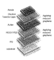
- FIG. 5( a ) is a schematic view of a general device structure of an organic solar cell
- FIG. 5( b ) is a current-voltage graph of the organic solar cell device
- FIG. 5( c ) is a table of device efficiency of the organic solar cell.
- FIG. 6 is a graph showing a long-term stability of the organic solar cell device in the case of applying the conventional PEDOT:PSS and in the case of applying the reduced graphene using p-toluene sulfonyl hydrazide as a buffer layer of the organic solar cell.
- a method for fabricating a graphene thin film comprises (a) preparing graphene oxide; (b) preparing graphene through reducing the graphene oxide by a sulfonyl hydrazide-based reducing agent; (c) preparing a graphene dispersed solution by dispersing the graphene into an organic solvent; and (d) fabricating a graphene thin film by applying the graphene dispersed solution.
- sulfonyl hydrazide which is a stable form of hydrazine, is prepared as a derivative.
- the sulfonyl hydrazide can be used stably to thereby induce a reaction with a hydrazide group and epoxy, aldehyde group which exist in graphene oxide, thus a reduced graphene dispersed solution having effective reducibility and high dispersibility can be prepared.
- graphene prepared by using the hydrazine derivatives can have excellent electrical characteristics through a reduction process of stable, environment-friendly graphene oxide.
- the graphene thin film formed thusly can replace PEDOT:PSS which is generally used as a buffer layer in the related art organic solar cell.
- the graphene oxide may be obtained by treating graphite with at least one of acidic solution which is selected from a group consisting of H 2 SO 4 , KMnO 4 , HCl, and HNO 3 , and in the acidic solution, H 2 SO 4 or KMnO 4 may be used additionally.
- acidic solution which is selected from a group consisting of H 2 SO 4 , KMnO 4 , HCl, and HNO 3 , and in the acidic solution, H 2 SO 4 or KMnO 4 may be used additionally.
- H 2 SO 4 or KMnO 4 may be used additionally.
- the present invention is not limited thereto.
- the sulfonyl hydrazide-based reducing agent may be a compound having a sulfonyl hydrazide substituent represented by Chemical Formula 1 shown below:
- A may be any one in Chemical Formula 2 (a) to (f) shown below:
- the organic solvent in step (c) may be any one selected from a group consisting of amides, alcohols, sulfoxides, propylene carbonate, and acetonitrile.
- a thickness of the graphene thin film fabricated according to an embodiment of the present invention may range from 0.5 nm to 10000 nm.
- a method for fabricating an optoelectronic device comprises (1) a step of forming a buffer layer, and (2) a step of forming an electrode layer, wherein the buffer layer and the electrode layer are formed according to the method for fabricating a graphene thin film.
- a buffer layer may be formed on one of an interface of a positive electrode and a photo-activation layer of the organic solar cell and an interface of a negative electrode and the photo-activation layer of the organic solar cell, or on both of the interfaces thereof.
- a buffer layer may be formed on any one of an interface of a positive electrode and a light emitting layer of the OLED or an interface of a negative electrode and the light emitting layer of the OLED, or on both interfaces thereof.
- polystyrene sulfonate (Mw 70,000 g/mol), potassium permanganate, methylene chloride (MC), N,N-dimethylformamide (DMF), hydrogen sulfonate (98%), p-toluenesulfonylhydrazide, propylene carbonate (PPC), dimethylsulfoxide (DMSO), and methanol were purchased from Sigma-Aldrich Corporation and used, and dialysis kig (molecular cutoff membrane MW: 2000 ⁇ 3000 g/mol) was purchased from spectrumlab. Ultrapure water (18.3 M ⁇ cm ⁇ 1 ) was purified from Human ultra Pure system and used.
- 0.1 g of graphene oxide prepared according to the Hummers method was dispersed in 100 mL of ultrapure water, 2 g of p-toluene sulfonyl hydrazide was dissolved in an 10 mL of ethanol, and then, mixed in graphene oxide dispersed solution.
- the mixed graphene oxide dispersed solution was reacted at 60° C. for a day, filtered out by using a poly tetrafluoroethylene (PTFE), and then, cleansed with ultrapure water, methanol, and methylene chloride.
- Black reduced graphene was put at a concentration of 2 ⁇ 3 mg/mL into DMF and dispersed for 10 minutes by 100 Watt power to prepare a reduced graphene dispersed solution.
- the reduced graphene dispersed solution obtained by dispersing reduced graphene in the DMF was applied to a glass substrate which had been subjected to a UV ozone (UV/O 3 ) treatment (for 20 minutes), an ITO-deposited glass substrate, or a silicon substrate by variably adjusting with coating speeds from 1000 rpm to 9000 rpm and forming a thin film, and then, the thin film was thermally treated at 100° C. for 10 minutes to form a reduced graphene thin film.
- UV ozone UV ozone
- Sheet resistance of the reduced graphene thin film as formed through 4 point probe system and conductivity of three portions (upper, middle, and lower portions) of the same were measured, and then, an average value was obtained. Also, a thickness of the formed thin film was measured through a thin film thickness measurement instrument (surface profiler), and conductivity of the thin film was measured.
- ATR-IR Fourier transform infrared
- XPS X-ray photoelectron spectroscopy
- Axis NOVA spectroscopy of Kratos analytical Co., Ltd. was used (aluminum negative electrode, 1486.9 eV, 600 W operation).
- UV spectrum Cary 1E model of Varian was used.
- AFM atomic force microscope
- FIG. 1( a ) is a schematic view showing a process of preparing reduced graphene through p-toluene sulfonyl hydrazide
- FIG. 1( b ) is an image of color change of a graphene oxide solution and a reduced graphene solution
- FIG. 1( c ) is a UV spectrum graph of the reduced graphene.
- FIG. 2( a ) is an AFM image of the graphene oxide
- FIG. 2( b ) is an AFM image of the reduced graphene through p-toluene sulfonyl hydrazide.
- a sheet of graphene oxide was measured to be 1 ⁇ 1.4 nm due to hydroxyl, aldehyde, epoxy, and carboxylic acid introduced to the surface of graphene.
- the thickness of the thin film was measured to be 1.3 nm.
- the thickness of graphene was reduced according to removal of the hydroxyl, epoxy, and aldehide functional groups covalently bonded to the surface of the reduced graphene according to the reduction reaction of the sulfonyl hydrazide-based reducing agent, while a factor of increasing the thickness of the graphene sheet due to a formation of hydrazone according to a chemical reaction between the sulfonyl hydrazide-based reducing agent and the functional groups enumerated above covalently bonded to the graphene worked together.
- FIG. 3( a ) is an infrared spectrum (ATR-IR) graph of graphene oxide and reduced graphene.
- ATR-IR infrared spectrum
- FIG. 3( a ) it is noted that a spectrum was generated by a —CH 3 functional group of the toluene group in the region 2, and in FIG. 3( b ), based on a generation of a peak of a nitrogen atom at 400 eV of the XPS data, it is noted that the p-toluene sulfonyl group was covalently bonded as an functional group.
- FIG. 4( a ) is a graph showing transmittance according to the number of times of spin-coating
- FIG. 4( b ) is an AFM image of the reduced graphene according to the number of times of coating. Accordingly, it was ascertained that a reduced graphene thin film which is uniform and whose thickness can be adjusted can be formed.
- FIG. 4( c ) is a graph showing the results obtained by measuring sheet resistance of the reduced thin film fabricated through the spin-coating method by a 4 point probe system
- FIG. 4( d ) is a graph showing correlation between a thin film thickness and transmittance.
- the sulfonyl hydrazide-based reducing agent of the present invention is a novel reducing agent that can replace the existing hydrazine-based reducing agent.
- the formation of the thin film with a uniform thickness according to an embodiment of the present invention is greatly advantageous.
- the method of preparing reduced graphene through the sulfonyl hydrazide-based reducing agent according to the present invention allow for a method for forming a graphene thin film which is uniform and whose thickness can be adjusted, and has a significant meaning in that it can solve the two problems of the hydrazine reducing agent.
- electrodes and buffer layers of various electronic devices can be formed, whereby a low-priced electronic device with high performance can be implemented.
- FIG. 5( a ) is a schematic view of a general device structure of an organic solar cell
- FIG. 5( b ) is a current-voltage graph regarding device performance of the organic solar cell when graphene oxide, the reduced graphene prepared by using p-toluene sulfonyl hydrazide, and the reduced graphene thin film reduced by hydrazine were introduced between the ITO and the photo-activation layer as a hole transport layer and a buffer layer, instead of PEDOT:PSS, and when the hole transport layer and the buffer layer are not introduced.
- the reduced graphene prepared by using p-toluene sulfonyl hydrazide was introduced as the hole transport layer and the buffer layer to the organic solar cell, the better or equal results were obtained in comparison to the case of introduction of the PEDOT:PSS, and this is because a thin film can be uniformly introduced on the entire surface of the substrate through the reduced graphene preparation method of the present invention, and energy level is positioned to be suitable for transport holes, and the reduced graphene reduced by p-toluene sulfonyl hydrazide has higher conductivity than that of the graphene oxide.
- the reduced graphene prepared by using p-toluene sulfonyl hydrazide according to an embodiment of the present invention is used as a material of the hole transport layer and the buffer layer, the reduced graphene can fundamentally replace currently used PEDOT:PSS.
- the reduced graphene according to an embodiment of the present invention can perfectly replace PEDOT:PSS used as a buffer layer of an organic solar cell and a light emitting diode.
- a graphene thin film is formed by using the reduced graphene thin film prepared through the present invention on a flexible polymer substrate made of a flexible (or bendable) polymer material such as poly(ethylene-terephthalate) (PET0, polyethylene naphthalate (PEN), polyimide (Kapton), polyether ether ketone (PEEK), polyether sulfone (PES), or polyether imide (PIE) through a solution process such as spin coating
- PET0 poly(ethylene-terephthalate)
- PEN polyethylene naphthalate
- PEEK polyimide
- PEEK polyether ether ketone
- PES polyether sulfone
- PIE polyether imide
- FIG. 5( c ) is a table of device efficiency of the organic solar cell.
- FIG. 6 is a graph showing stability of an organic solar cell device over time when PEDOT:PSS was introduced, and when PEDOT:PSS was not introduced, and when p-toluene sulfonyl hydrazide was introduced by thickness. It can be seen that, when p-toluene sulfonyl hydrazide was introduced, surface roughness was reduced, neutrality characteristics were obtained, and air or moisture was prevented from passing through, so a life span of the device was drastically increased, in comparison to PEDOT:PSS. This is a solution that can stably drive the device and significantly enhance a life span thereof at a timing when a long-term stability of the organic solar cell device is problematic.
Landscapes
- Chemical & Material Sciences (AREA)
- Engineering & Computer Science (AREA)
- Nanotechnology (AREA)
- Materials Engineering (AREA)
- Physics & Mathematics (AREA)
- Crystallography & Structural Chemistry (AREA)
- Organic Chemistry (AREA)
- General Physics & Mathematics (AREA)
- Condensed Matter Physics & Semiconductors (AREA)
- Inorganic Chemistry (AREA)
- Composite Materials (AREA)
- Manufacturing & Machinery (AREA)
- Mathematical Physics (AREA)
- Theoretical Computer Science (AREA)
- Photovoltaic Devices (AREA)
- Carbon And Carbon Compounds (AREA)
Abstract
Description


Claims (9)


Applications Claiming Priority (2)
| Application Number | Priority Date | Filing Date | Title |
|---|---|---|---|
| KR1020110007470A KR101240276B1 (en) | 2011-01-25 | 2011-01-25 | A preparation method for reduced graphene oxide using the sulfonyl hydrazide-based reducing agent and optoelectronic devices thereof |
| KR10-2011-0007470 | 2011-01-25 |
Publications (2)
| Publication Number | Publication Date |
|---|---|
| US20120190139A1 US20120190139A1 (en) | 2012-07-26 |
| US8865515B2 true US8865515B2 (en) | 2014-10-21 |
Family
ID=46544462
Family Applications (1)
| Application Number | Title | Priority Date | Filing Date |
|---|---|---|---|
| US13/356,965 Expired - Fee Related US8865515B2 (en) | 2011-01-25 | 2012-01-24 | Preparation method for reduced graphene oxide using sulfonyl hydrazide-based reducing agent and optoelectronic devices thereof |
Country Status (2)
| Country | Link |
|---|---|
| US (1) | US8865515B2 (en) |
| KR (1) | KR101240276B1 (en) |
Cited By (2)
| Publication number | Priority date | Publication date | Assignee | Title |
|---|---|---|---|---|
| US10014440B2 (en) * | 2015-11-24 | 2018-07-03 | Shenzhen China Star Optoelectronics Technology Co., Ltd. | Graphene display devices and the display driving methods thereof |
| RU224254U1 (en) * | 2023-12-16 | 2024-03-19 | Федеральное государственное бюджетное образовательное учреждение высшего образования "Кемеровский государственный университет" | INSTALLATION FOR VAPOR PHASE RECOVERY OF GRAPHENE OXIDE DISPERSIONS |
Families Citing this family (21)
| Publication number | Priority date | Publication date | Assignee | Title |
|---|---|---|---|---|
| KR101240276B1 (en) * | 2011-01-25 | 2013-03-07 | 한국과학기술연구원 | A preparation method for reduced graphene oxide using the sulfonyl hydrazide-based reducing agent and optoelectronic devices thereof |
| US9360905B2 (en) * | 2012-04-09 | 2016-06-07 | Nanotek Instruments, Inc. | Thermal management system containing an integrated graphene film for electronic devices |
| KR101381318B1 (en) * | 2012-08-09 | 2014-04-14 | 한국기계연구원 | Preparing method of graphene films using fullerene derivative |
| KR101969851B1 (en) * | 2012-10-08 | 2019-04-17 | 삼성전자주식회사 | Method for preparation of reduced graphene oxide and reduced graphene oxide-polymer composite |
| US9899120B2 (en) | 2012-11-02 | 2018-02-20 | Nanotek Instruments, Inc. | Graphene oxide-coated graphitic foil and processes for producing same |
| CN103310905A (en) * | 2012-11-08 | 2013-09-18 | 电子科技大学 | Method for manufacturing nano-composite conductive thin film and nano-composite conductive thin film |
| US9533889B2 (en) | 2012-11-26 | 2017-01-03 | Nanotek Instruments, Inc. | Unitary graphene layer or graphene single crystal |
| KR101430650B1 (en) | 2013-01-11 | 2014-08-19 | 경희대학교 산학협력단 | Photodetector |
| US10566482B2 (en) | 2013-01-31 | 2020-02-18 | Global Graphene Group, Inc. | Inorganic coating-protected unitary graphene material for concentrated photovoltaic applications |
| US10087073B2 (en) | 2013-02-14 | 2018-10-02 | Nanotek Instruments, Inc. | Nano graphene platelet-reinforced composite heat sinks and process for producing same |
| KR101650705B1 (en) * | 2013-05-21 | 2016-08-24 | 한국화학연구원 | Organic light emitting diode using graphene oxide, and the fabrication method threrof |
| US9236156B2 (en) * | 2013-10-18 | 2016-01-12 | Snu R&Db Foundation | Preparing method of reduced graphene oxide film using a chemical reduction method and a pressure-assisted thermal reduction method, reduced graphene oxide film prepared by the same, and graphene electrode including the reduced graphene oxide film |
| CN103700513B (en) * | 2013-12-30 | 2016-09-14 | 中山大学 | A kind of graphene paper and its preparation method and application |
| US9761443B2 (en) * | 2014-01-31 | 2017-09-12 | The Regents Of The University Of California | Method for passivating surfaces, functionalizing inert surfaces, layers and devices including same |
| KR101664979B1 (en) * | 2015-06-19 | 2016-10-11 | 서울대학교산학협력단 | Preparing method of reduced graphene oxide film, reduced graphene oxide film prepared by the same, and graphene electrode including the reduced graphene oxide film |
| KR101865997B1 (en) * | 2015-07-24 | 2018-06-08 | 현대자동차주식회사 | Electrode protection layer for the dye-sensitized solar cell and method of forming the same |
| KR102009245B1 (en) * | 2017-05-31 | 2019-08-09 | 부경대학교 산학협력단 | Polymer solar cell having cathode buffer layer including novel small molecular electrolytes |
| CN108467028B (en) * | 2018-04-26 | 2021-10-12 | 上海大学 | Preparation method and application of intelligent graphene quantum dot cluster |
| CN109671846B (en) * | 2018-11-23 | 2023-02-10 | 上海工程技术大学 | Perovskite solar cells with three-dimensional structured graphene as back electrode and its preparation |
| WO2021123929A1 (en) * | 2019-12-18 | 2021-06-24 | ALIWARGA, Harry Kasuma | Method of manufacturing hard solar cell through printing process and hard solar cell thereof |
| CN115595051B (en) * | 2022-08-11 | 2023-12-05 | 浙江创赢新材料有限公司 | Preparation method of two-component coating composition |
Citations (3)
| Publication number | Priority date | Publication date | Assignee | Title |
|---|---|---|---|---|
| KR20100121978A (en) | 2009-05-11 | 2010-11-19 | 울산대학교 산학협력단 | Methods for fabricating the thin film graphene |
| US20120190139A1 (en) * | 2011-01-25 | 2012-07-26 | Korea Institute Of Science And Technology | Preparation method for reduced graphene oxide using sulfonyl hydrazide-based reducing agent and optoelectronic devices thereof |
| US20130314844A1 (en) * | 2012-05-23 | 2013-11-28 | Nanyang Technological University | Method of preparing reduced graphene oxide foam |
-
2011
- 2011-01-25 KR KR1020110007470A patent/KR101240276B1/en not_active Expired - Fee Related
-
2012
- 2012-01-24 US US13/356,965 patent/US8865515B2/en not_active Expired - Fee Related
Patent Citations (3)
| Publication number | Priority date | Publication date | Assignee | Title |
|---|---|---|---|---|
| KR20100121978A (en) | 2009-05-11 | 2010-11-19 | 울산대학교 산학협력단 | Methods for fabricating the thin film graphene |
| US20120190139A1 (en) * | 2011-01-25 | 2012-07-26 | Korea Institute Of Science And Technology | Preparation method for reduced graphene oxide using sulfonyl hydrazide-based reducing agent and optoelectronic devices thereof |
| US20130314844A1 (en) * | 2012-05-23 | 2013-11-28 | Nanyang Technological University | Method of preparing reduced graphene oxide foam |
Non-Patent Citations (2)
| Title |
|---|
| Bin Yin, et al; "Buffer Layer of PEDOT:PSS/Graphene Composite for Polymer Solar Cells", Journal of Nanoscience and Nanotechnology, vol. 10, No. 3, Mar. 2010; pp. 1934-1938 abstract only. |
| Jin-Mun Yun, et al; "Facile and rapid reduction of graphene oxide using p-toluenesul fonylhydrazide reagent via microwave irradiation", 2010, IUMRS-ICEM 2010, (Aug. 22, 2010) 161 pages. |
Cited By (2)
| Publication number | Priority date | Publication date | Assignee | Title |
|---|---|---|---|---|
| US10014440B2 (en) * | 2015-11-24 | 2018-07-03 | Shenzhen China Star Optoelectronics Technology Co., Ltd. | Graphene display devices and the display driving methods thereof |
| RU224254U1 (en) * | 2023-12-16 | 2024-03-19 | Федеральное государственное бюджетное образовательное учреждение высшего образования "Кемеровский государственный университет" | INSTALLATION FOR VAPOR PHASE RECOVERY OF GRAPHENE OXIDE DISPERSIONS |
Also Published As
| Publication number | Publication date |
|---|---|
| KR20120086177A (en) | 2012-08-02 |
| KR101240276B1 (en) | 2013-03-07 |
| US20120190139A1 (en) | 2012-07-26 |
Similar Documents
| Publication | Publication Date | Title |
|---|---|---|
| US8865515B2 (en) | Preparation method for reduced graphene oxide using sulfonyl hydrazide-based reducing agent and optoelectronic devices thereof | |
| Gogotsi | The future of MXenes | |
| Huang et al. | Effective work function modulation of graphene/carbon nanotube composite films as transparent cathodes for organic optoelectronics | |
| Deng et al. | Niobium‐Carbide MXene Modified Hybrid Hole Transport Layer Enabling High‐Performance Organic Solar Cells Over 19% | |
| Kwon et al. | Extremely stable graphene electrodes doped with macromolecular acid | |
| Wang et al. | Thiol–ene cross-linked polymer gate dielectrics for low-voltage organic thin-film transistors | |
| Withers et al. | Nanopatterning of fluorinated graphene by electron beam irradiation | |
| Li et al. | Graphene nano-“patches” on a carbon nanotube network for highly transparent/conductive thin film applications | |
| Zhang et al. | Al-TiO2 composite-modified single-layer graphene as an efficient transparent cathode for organic solar cells | |
| Su et al. | The application of graphene derivatives in perovskite solar cells | |
| Beaumont et al. | Increased efficiency in small molecule organic photovoltaic cells through electrode modification with self-assembled monolayers | |
| Lien et al. | Effect of copper oxide oxidation state on the polymer-based solar cell buffer layers | |
| Seo et al. | Study of cooling rate on the growth of graphene via chemical vapor deposition | |
| An et al. | Ultraclean transfer of CVD-grown graphene and its application to flexible organic photovoltaic cells | |
| Mattevi et al. | Solution-processable organic dielectrics for graphene electronics | |
| JP2013112604A (en) | Graphene nano-sheet and method for producing the same | |
| Cho et al. | Effects of ultraviolet–ozone treatment on organic-stabilized ZnO nanoparticle-based electron transporting layers in inverted polymer solar cells | |
| Guo et al. | Large-area metal–semiconductor heterojunctions realized via MXene-induced two-dimensional surface polarization | |
| Park et al. | An Alternative Hole Transport Layer for Both ITO-and Graphene-Based Organic Solar Cells. | |
| Han et al. | Enhanced electrical properties of reduced graphene oxide multilayer films by in-situ insertion of a TiO2 layer | |
| Duan et al. | High-performance flexible Ag nanowire electrode with low-temperature atomic-layer-deposition fabrication of conductive-bridging ZnO film | |
| Dang et al. | Solution processed hybrid Graphene-MoO3 hole transport layers for improved performance of organic solar cells | |
| JP2012156501A (en) | Semiconductor composition | |
| Song et al. | Enhanced performance and stability of PEDOT: PSS Thin-Film thermoelectrics by De-doping with Nitrogen-Doped graphene quantum Dots | |
| Mumthas et al. | The γ-radiated g-C3N4 additive for highly conductive electron transport layer in polymer solar cells |
Legal Events
| Date | Code | Title | Description |
|---|---|---|---|
| AS | Assignment |
Owner name: KOREA INSTITUTE OF SCIENCE AND TECHNOLOGY, KOREA, Free format text: ASSIGNMENT OF ASSIGNORS INTEREST;ASSIGNORS:NA, SEOK IN;KIM, DONG YU;KOO, HYE YOUNG;AND OTHERS;REEL/FRAME:027585/0485 Effective date: 20120118 |
|
| AS | Assignment |
Owner name: FISONIC HOLDING LIMITED, CYPRUS Free format text: ASSIGNMENT OF ASSIGNORS INTEREST;ASSIGNOR:FISENKO, VLADIMIR VLADIMIROVICH, MR.;REEL/FRAME:027953/0879 Effective date: 20120321 |
|
| STCF | Information on status: patent grant |
Free format text: PATENTED CASE |
|
| FEPP | Fee payment procedure |
Free format text: PAYOR NUMBER ASSIGNED (ORIGINAL EVENT CODE: ASPN); ENTITY STATUS OF PATENT OWNER: SMALL ENTITY |
|
| MAFP | Maintenance fee payment |
Free format text: PAYMENT OF MAINTENANCE FEE, 4TH YR, SMALL ENTITY (ORIGINAL EVENT CODE: M2551) Year of fee payment: 4 |
|
| FEPP | Fee payment procedure |
Free format text: MAINTENANCE FEE REMINDER MAILED (ORIGINAL EVENT CODE: REM.); ENTITY STATUS OF PATENT OWNER: SMALL ENTITY |
|
| LAPS | Lapse for failure to pay maintenance fees |
Free format text: PATENT EXPIRED FOR FAILURE TO PAY MAINTENANCE FEES (ORIGINAL EVENT CODE: EXP.); ENTITY STATUS OF PATENT OWNER: SMALL ENTITY |
|
| STCH | Information on status: patent discontinuation |
Free format text: PATENT EXPIRED DUE TO NONPAYMENT OF MAINTENANCE FEES UNDER 37 CFR 1.362 |
|
| FP | Lapsed due to failure to pay maintenance fee |
Effective date: 20221021 |